Switching Regulator Noise: Comprehensive Understanding and Analysis

LDO basics: Power Supply Rejection Ratio (PSRR)
| Topics covered in this article: |
| Ⅰ. Introduction |
| Ⅱ. Switching Ripple Noise |
| Ⅲ. Broadband Noise |
| Ⅳ. High Frequency Spikes and Ringing |
| Ⅴ. Switching Regulator PSRR |
| Ⅵ. Summary |
Ⅰ. Introduction
When compared to the output of a low dropout (LDO) regulator, the output voltage of a standard switching regulator is considered to be fairly loud. The LDO voltage, on the other hand, might cause substantial additional thermal issues and complicate power supply design. To help build low-noise switching solutions that deliver low-noise performance equivalent to LDO regulators, a full understanding of switching regulator noise is required. The buck regulator with current mode control, which is the most widely employed in applications, is the subject of this article's examination and evaluation. Switching ripple noise, current broadband noise features (and their origins), and switching-induced high-frequency spikes are all studied using signal analysis. This article will discuss switching regulator PSRR (Power Supply Rejection Ratio, which is important for input noise rejection) and signal analysis methods.
Ⅱ. Switching Ripple Noise
Based on fundamental and harmonic theory, this section introduces the formula for estimating the output ripple of a buck converter . Because the peak-to-peak voltage amplitude in a switching regulator is typically a few mV to tens of mV, depending on the switching regulator topology and fundamental function, ripple is always the main noise. It should be regarded as a reliable and periodic signal. An oscilloscope in the time domain or Fourier decomposition in the frequency domain can easily identify and quantify it if it operates at a set switching frequency.

Buck Regulator Topology
A common buck regulator is depicted above. The two switches are alternately turned on and off, resulting in a perfect square wave at the SW node voltage VSW, which is then translated to the duty cycle and input voltage. The following formula can be used to calculate VSW:

VSW Formula Representation
The input voltage is denoted by VIN . The duty cycle is equal to VOUT/VIN for a buck regulator. The fundamental and harmonic components of VSW are only dependent on the duty cycle once VIN has been calculated. The VSW fundamental and harmonic amplitudes are shown against the duty cycle in figure below. The fundamental wave dominates the ripple amplitude when the duty cycle is close to half.

Buck Regulator VSW Amplitude vs. Duty Cycle
The output LC stage transfer function of a buck regulator is as follows:

LC Level Transfer Function
L stands for output inductance, DCR stands for inductance resistance, and CL stands for inductance parallel capacitance. The output capacity value is COUT. The capacitor series inductance value is denoted by ESL. The ESR is the value of the capacitor's series resistance. As a result, VOUT can be written as follows:

The Formula for VOUT
To make the computations easier, we'll use a 20 dB/decade output LC stage, followed by the VOUT ripple fundamental and harmonic amplitudes proportional to the duty cycle, as illustrated in figure below. The third or odd harmonics will be higher than the even harmonics when the duty cycle is close to half. Higher harmonics will have smaller amplitudes and a very small share of the total ripple amplitude due to LC suppression. In the switching regulator output ripple, the fundamental amplitude is also the main component.

Buck Regulator VOUT Ripple Amplitude vs. Duty Cycle
The input voltage, duty cycle, switching frequency, and LC stage all affect the fundamental amplitude of a buck regulator; nevertheless, all of these parameters affect application requirements like as efficiency and solution size. It is advised that a post-filter be used to further decrease the ripple.
Ⅲ. Broadband Noise
Broadband noise on the output voltage of switching regulators is random amplitude noise. It can be stated in V/Hz, which is inseparable from the noise density over the frequency range, or in V rms, which is inseparable from the noise density over the frequency range. Broadband noise is primarily found in the 10 Hz to 1 MHz frequency range of the switching regulator due to restrictions in the silicon process and reference filter design, and it is difficult to minimize it by adding filters in the low frequency region.
The peak-to-peak amplitude voltage of a typical buck regulator is around 100V to 1000V, which is substantially lower than switching ripple noise.Broadband noise can become the main noise in the switching regulator's output voltage if additional filters are applied to reduce switching ripple noise.
Switching ripple is the main source of output noise for a buck regulator when there is no extra filter, as seen in the figure below. When additional filters are utilized, the predominant source of output noise is wideband noise, as seen in the figure below.

VOUT without additional filter

VOUT with Extra Filter (Measured with 1000x Preamp)
The regulator control scheme and module noise information must be gathered in order to identify and analyze switching regulator output broadband noise. Figure below depicts a common current-mode buck regulator control method with block noise source injection as an example.

Typical Current Mode Buck Regulator Control Scheme
There are two types of noise in the acquired control loop transfer function and block noise characteristic information: loop input noise and in-loop noise. Noise in the loop input is sent to the output within the control loop bandwidth, while noise outside the loop bandwidth is attenuated. Because unity feedback gain keeps the noise level constant rather than increasing as the output voltage level grows, creating low noise EAs and references is crucial for switching regulators. The most difficult task is identifying the major source of noise in the system and decreasing it in the circuit design. The ADP5014 combines a current-mode control method and a simple LC external filter to produce sub-20V rms noise performance spanning the 10Hz to 1 MHz frequency range, making it ideal for low-noise technology. Figure below depicts the ADP5014's output noise performance.

ADP5014 Output Noise Performance with Additional LC Filter
Ⅳ. High Frequency Spikes and Ringing
Because the output voltage is generated by the switching regulator turn-on or turn-off transients, the third type of noise is high frequency spikes and ringing noise. Fast current transients in buck regulators will create high frequency voltage spikes and ringing at the SW node due to parasitic inductance and capacitance in silicon circuits and PCB traces. The present load increases the spike and ringing sounds. Figure below depicts the formation of a spike by a buck regulator. The maximum peaking and ringing frequencies will be in the 20 MHz to 300 MHz region, depending on the switching regulator's on/off slew rate, and the output LC filter may not be particularly effective in rejection due to parasitic inductance and capacitance. In comparison to all of the previously discussed conduction channels, the radiated noise from the SW and VIN nodes is the worst; the output voltage and other analog circuits suffer as a result of its extremely high frequency.

Buck Regulator High-Frequency Spikes and Ringing Noise
Effective solutions for application and chip design implementation are advised to eliminate high-frequency spikes and ringing noise. On the termination load, an extra LC filter or bead should be utilized first. The spike noise on the output is often considerably smaller than the ripple noise, but it adds higher frequency components. Second, noise sources at the SW and input nodes should be insulated or kept away from sensitive analog circuits on the output side, as well as the output inductor. The design relies heavily on careful placement and routing. Third, reduce the SW node noise by optimizing the switching regulator's on/off slew rate and minimizing the parasitic inductance and resistance. Through chip design, ADI Silent Switcher® technology also helps to reduce VIN node noise.
Ⅴ. Switching Regulator PSRR
PSRR measures a switching regulator's ability to prevent input power supply noise from reaching the output. The PSRR performance of the buck regulator in the low-frequency band is examined in this section. The radiated path, rather than the conduction path, is where high-frequency noise has the most impact on the output voltage.

Current Mode Buck Small Signal Diagram from Input Voltage to Output
According to the buck small-signal diagram shown above, the buck PSRR can be expressed as follows:

PSRR Representation
In it:

PSRR Representation2
Fm is the slope gain
F g is the control input voltage
Rcs is the current detection gain
Zo(s) is the output capacitance and load
Tv(s) is the loop transfer function

PSRR Calculation Results Using Buck Small Signal Mode

PSRR Simulation in SIMPLIS Mode
Compare the simulation findings to the signal mode calculations. The small-signal mode is correct, and the modeling results support that.
A switching regulator's PSRR is determined by the loop gain performance in the low-frequency range. Input noise in the IF range is rejected by the switching regulator's built-in LC filter (100 Hz to 10 MHz). In this range, the rejection performance is substantially better than the LDO PSRR, Switching regulators provide optimum PSRR performance at low frequencies because of their large loop gain, whereas the inherent LC filter impairs the mid-frequency range.
Ⅵ. Summary
Analog circuits such as ADC /DAC, clocks, and PLLs are increasingly requiring clean, high-current power sources. In different frequency bands, each device has varied requirements and regulations for power supply noise. To design and implement high efficiency, low noise switching regulators that fulfill the low noise parameters of most analog circuit power supplies, a full grasp of the many types of switching regulator noise and awareness of power supply noise requirements is required. This low noise switching solution will have a higher power efficiency, a smaller solution
1. Can a switching regulator convert DC to AC?
Yes, it can. Generally, the switching power supply first rectifies the AC directly into DC, and then modulates the DC into a pulse waveform, and then transforms, rectifies and filters to obtain a relatively straight DC. Inverter power supply is a typical switching power supply that converts DC into AC.
2. What is a switching regulator?
The switching regulator has a negative feedback sampling circuit at the output end of the switching power supply, which can play a role in regulating the voltage. Usually, the switching power supply has higher efficiency, larger input dynamic range and better dynamic response, so it is widely used now.
3. What are the respective advantages of linear regulators and switching regulators?
The advantages of linear regulators are smooth output with low ripple and noise. The disadvantage is that the efficiency is low, and the greater the pressure difference, the lower the efficiency.
The advantage of the switching regulator is high efficiency, but the disadvantage is that the switching process generates high-order harmonics, resulting in large output ripple and noise.
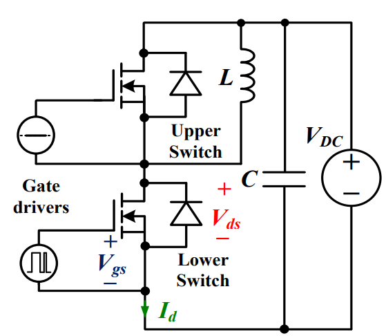
 Discovering New and Advanced Methodology for Determining the Dynamic Characterization of Wide Bandgap DevicesSaumitra Jagdale15 March 20242507
For a long era, silicon has stood out as the primary material for fabricating electronic devices due to its affordability, moderate efficiency, and performance capabilities. Despite its widespread use, silicon faces several limitations that render it unsuitable for applications involving high power and elevated temperatures. As technological advancements continue and the industry demands enhanced efficiency from devices, these limitations become increasingly vivid. In the quest for electronic devices that are more potent, efficient, and compact, wide bandgap materials are emerging as a dominant player. Their superiority over silicon in crucial aspects such as efficiency, higher junction temperatures, power density, thinner drift regions, and faster switching speeds positions them as the preferred materials for the future of power electronics.
Read More A Comprehensive Guide to FPGA Development BoardsUTMEL11 September 202515944
This comprehensive guide will take you on a journey through the fascinating world of FPGA development boards. We’ll explore what they are, how they differ from microcontrollers, and most importantly, how to choose the perfect board for your needs. Whether you’re a seasoned engineer or a curious hobbyist, prepare to unlock new possibilities in hardware design and accelerate your projects. We’ll cover everything from budget-friendly options to specialized boards for image processing, delve into popular learning paths, and even provide insights into essential software like Vivado. By the end of this article, you’ll have a clear roadmap to navigate the FPGA landscape and make informed decisions for your next groundbreaking endeavor.
Read More Applications of FPGAs in Artificial Intelligence: A Comprehensive GuideUTMEL29 August 20253878
This comprehensive guide explores FPGAs as powerful AI accelerators that offer distinct advantages over traditional GPUs and CPUs. FPGAs provide reconfigurable hardware that can be customized for specific AI workloads, delivering superior energy efficiency, ultra-low latency, and deterministic performance—particularly valuable for edge AI applications. While GPUs excel at parallel processing for training, FPGAs shine in inference tasks through their adaptability and power optimization. The document covers practical implementation challenges, including development complexity and resource constraints, while highlighting solutions like High-Level Synthesis tools and vendor-specific AI development suites from Intel and AMD/Xilinx. Real-world applications span telecommunications, healthcare, autonomous vehicles, and financial services, demonstrating FPGAs' versatility in mission-critical systems requiring real-time processing and minimal power consumption.
Read More 800G Optical Transceivers: The Guide for AI Data CentersUTMEL24 December 20254719
The complete guide to 800G Optical Transceiver standards (QSFP-DD vs. OSFP). Overcome supply shortages and scale your AI data center with Utmel Electronic.
Read More The 2026 Engineer’s Guide: Choosing the Right MCU for Your Next IoT & New Energy ProjectUTMEL30 April 202664
A comprehensive comparison of 2026's leading MCUs from ST, NXP, and Microchip across power efficiency, processing performance, connectivity, and ecosystems to help engineers select the optimal chip for next-gen IoT and new energy projects.
Read More
Subscribe to Utmel !
![ATSHA204A-MAHDA-S]() ATSHA204A-MAHDA-S
ATSHA204A-MAHDA-SMicrochip Technology
![HCS360-I/SN]() HCS360-I/SN
HCS360-I/SNMicrochip Technology
![AT88SC0204CA-SH]() AT88SC0204CA-SH
AT88SC0204CA-SHMicrochip Technology
![CS8190EDWFR20G]() CS8190EDWFR20G
CS8190EDWFR20GON Semiconductor
![ATECC608A-MAHDA-T]() ATECC608A-MAHDA-T
ATECC608A-MAHDA-TMicrochip Technology
![ATSHA204A-MAHCZ-T]() ATSHA204A-MAHCZ-T
ATSHA204A-MAHCZ-TMicrochip Technology
![HCS301/SN]() HCS301/SN
HCS301/SNMicrochip Technology
![AT88SC0808CA-Y6H-T]() AT88SC0808CA-Y6H-T
AT88SC0808CA-Y6H-TMicrochip Technology
![ATAES132A-SHEQ-T]() ATAES132A-SHEQ-T
ATAES132A-SHEQ-TMicrochip Technology
![HCS201-I/P]() HCS201-I/P
HCS201-I/PMicrochip Technology


 Product
 Brand
Brand Articles
 Tools
Tools


