

 Product
 Brand
Brand Articles
 Tools
Tools
Sourcing Silicon Capacitors and MLCCs in the AI Hardware Era
Quick Answer: Modern artificial intelligence hardware requires a multi-tiered Power Delivery Network (PDN) where Deep Trench Capacitors (DTCs) and Multilayer Ceramic Capacitors (MLCCs) operate as complementary components[1] rather than direct replacements.
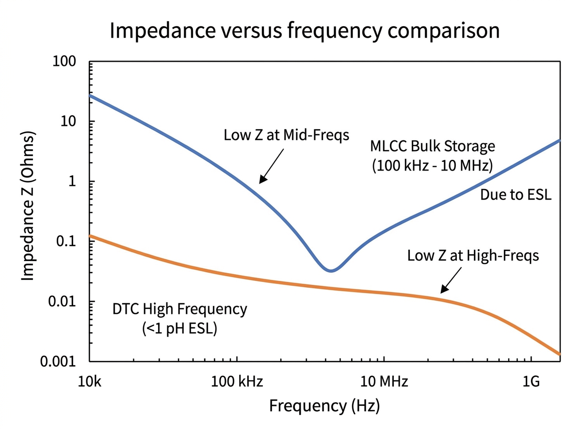
Deep Trench Silicon Capacitors (DTCs) manage rapid, high-frequency transient current steps (di/dt) directly at the package, interposer, or near-die level. Their semiconductor construction allows ultra-thin profiles, stable performance under applied DC voltage, and sub-picohenry class Equivalent Series Inductance (ESL) when integrated with optimized micro-bump layouts[2].
Multilayer Ceramic Capacitors (MLCCs) deliver bulk energy storage and mid-frequency decoupling (100 kHz to 10 MHz) on the printed circuit board (PCB) due to their superior capacitance-per-dollar ratio and high volumetric storage.
Engineering Decision Rule: Deploy DTCs inside advanced package substrate cavities or silicon interposers when space is constrained and parasitic loop inductance must be minimized. Deploy high-density Class II MLCCs on the motherboard to absorb lower-frequency energy ripples and maintain bulk supply stability.
The AI Power Integrity Challenge: di/dt and Near-Die Decoupling
TL;DR Answer: High-performance AI accelerators require thousands of amperes at core voltages under 1.0V, creating transient current slew rates (di/dt) that induce fatal voltage droops across parasitic loop inductances if decoupling is restricted to board-level components.
As artificial intelligence workloads scale, neural processing units (NPUs) and high-performance computing (HPC) processors demand extreme current levels at core supply voltages (VDD) typically dropping below 0.8V to 1.0V. Continuous currents can exceed 1,000A to 4,000A+, while rapid transitions between idle and full tensor compute states generate transient current slew rates (di/dt) exceeding 1,000 A/µs.
According to basic power integrity principles, parasitic inductance (L) along the power delivery path induces a transient voltage drop (ΔV) given by:
ΔV = I · R + L · (di/dt)
In sub-1V supply rails, allowable noise margins are tight—often constrained within ±3% to ±5%[4] (a window of less than 30 mV to 50 mV). If transient voltage droop exceeds this tolerance, timing violations occur across logic gates, resulting in bit errors, calculation instability, or system crashes.
Understanding these sub-1V core logic constraints and power delivery network bottlenecks is essential when evaluating advanced semiconductor delivery structures, such as those analyzed in The BSPDN Revolution: Overcoming IR Drop in Sub-2nm GAAFET.
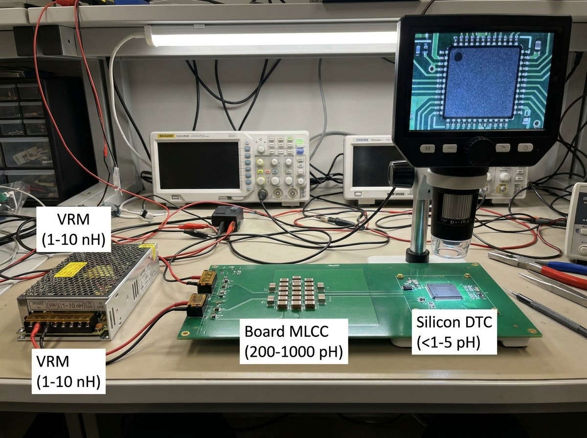
The PDN Inductance Hierarchy
Traditional power delivery networks relied on surface-mount MLCCs placed on the motherboard. However, physical distance between board-mounted passives and the processor die introduces unavoidable parasitic loop inductance:
| PDN Tier | Location / Domain | Typical Parasitic Loop Inductance | Primary Decoupling Function |
|---|---|---|---|
| Voltage Regulator Module (VRM) | Motherboard Power Plane | 1 nH to 10 nH+ | Low-frequency regulation (<100 kHz) |
| Board-Level MLCCs | Motherboard Surface (SMT) | 200 pH to 1,000 pH | Bulk charge storage & mid-frequency filtering (100 kHz–10 MHz) |
| Package BGA Via Stack | Package Substrate Interface | 100 pH to 500 pH | Structural transition boundary |
| Package / Interposer DTCs | Substrate Cavity / Silicon Interposer | <1 pH to 5 pH (layout dependent) | Near-die high-frequency transient suppression (>10 MHz) |
Because high PCB and BGA inductances decouple board-mounted MLCCs from the compute silicon during sub-nanosecond load spikes, board-level passives cannot respond fast enough to prevent localized switching noise. To solve this, power integrity architects integrate silicon-based decoupling components within the package substrate or silicon interposer.
The Physics of Deep Trench Capacitors (DTC)
TL;DR Answer: Deep Trench Silicon Capacitors achieve high volumetric capacitance in ultra-thin form factors by using semiconductor fabrication equipment to etch high-aspect-ratio 3D microstructures into monocrystalline silicon[3], covered by atomic layer deposition of high-k dielectrics.
Unlike traditional MLCCs—fabricated by stacking ceramic dielectric sheets with screen-printed metal pastes before sintering in a high-temperature furnace—Deep Trench Capacitors (DTCs) are manufactured using standard semiconductor wafer fabrication processes.
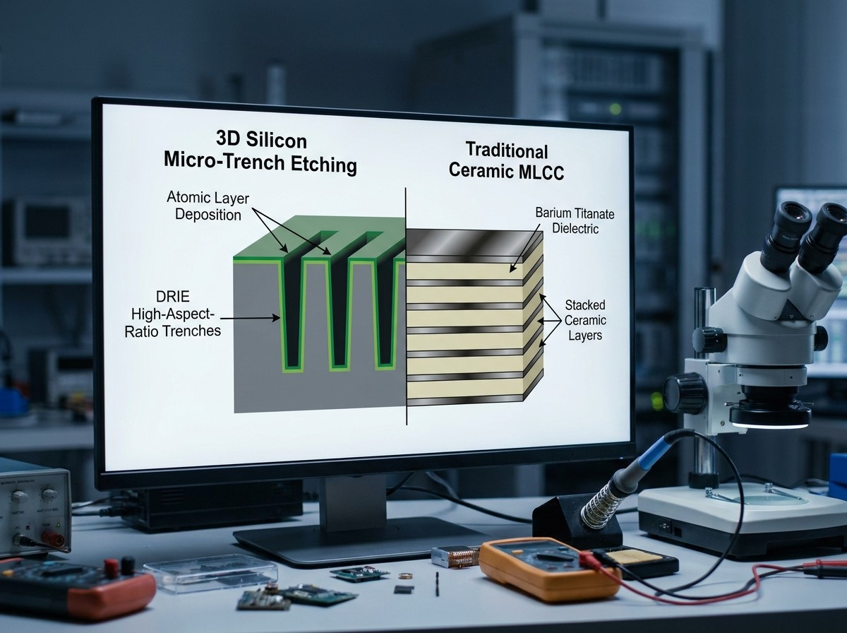
Fabrication Comparison: Silicon Fabrication vs. Ceramic Sintering
| Manufacturing Step | Deep Trench Silicon Capacitors (DTC) | Standard Class II MLCCs |
|---|---|---|
| Substrate Material | Single-crystal monocrystalline silicon wafer | Barium titanate (BaTiO3) ceramic powder slurry |
| Surface Magnification | Bosch Deep Reactive-Ion Etching (DRIE) of 3D trenches | Stacking multiple flat dielectric and electrode sheets |
| Dielectric Deposition | Atomic Layer Deposition (ALD) of uniform high-k thin films | High-temperature kiln sintering (>1,000°C) |
| Structure Purity | Amorphous dielectric layer; no grain boundaries | Polycrystalline structure with internal grain boundaries |
| Form Factor / Profile | Ultra-thin profiles (achievable <100 µm) | Discrete rectangular SMT chip (0.3 mm to 2.5 mm+) |
1. High-Aspect-Ratio 3D Microstructures
DTCs overcome planar area limitations by using Deep Reactive-Ion Etching (DRIE) to etch millions of vertical micro-trenches directly into the silicon substrate. By creating aspect ratios ranging from 20:1 to over 50:1, manufacturers multiply the effective capacitive surface area per unit of footprint without increasing physical dimensions.
2. Atomic Layer Deposition (ALD)
After trench etching, Atomic Layer Deposition (ALD) coats the 3D structures with atomic-level uniformity. High-k dielectric thin films (such as HfO2, Al2O3, or multi-layer dielectric stacks) are grown layer by layer. Because ALD provides pinhole-free step coverage over high-aspect-ratio trenches, these dielectrics support high breakdown voltages while maximizing charge storage per unit area.
3. Densities Reported in Research
In academic research and industry process announcements, advanced deep trench silicon designs have reported capacitance densities ranging from 1,000 nF/mm² up to 3,500 nF/mm² in specialized implementations. Note that these figures come from research and process announcements, not from commercial datasheet guarantees. In commercial applications, exact achievable density depends on target breakdown voltage requirements and process thermal budgets.
DTCs vs. MLCCs: A Complementary PDN Architecture
TL;DR Answer: DTCs provide ultra-low inductance and voltage-stable performance for package-level transient suppression, while MLCCs provide high-capacity, cost-effective bulk energy storage on the motherboard.
DTCs and MLCCs are optimized for different frequency domains and physical tiers of the power delivery network. The table below highlights their key operational trade-offs:
| Parameter / Feature | Deep Trench Silicon Capacitors (DTC) | Standard Class II MLCCs (X5R / X7R) |
|---|---|---|
| Primary PDN Function | High-frequency transient suppression | Bulk energy storage & low/mid-frequency filtering |
| Typical Physical Domain | Inside package, silicon interposer, or under-die | Motherboard / PCB expansion cards |
| Equivalent Series Inductance (ESL) | Sub-picohenry class (<1 pH achievable in optimized layouts) | 200 pH to 1,000 pH (dependent on case size & mounting) |
| DC Bias Sensitivity | Negligible capacitance drop across rated VDC | Significant capacitance drop (50% or more loss under load) |
| Thermal Stability | Minimal drift across operating ranges (e.g., -55°C to +150°C) | Capacitance drifts up to ±15% standard range |
| Form Factor Profile | Ultra-thin (<100 µm reported in thin-film formats) | Standard discrete heights (0.3 mm to 2.5 mm+) |
| Relative Unit Cost | Higher unit cost; reserved for package integration | High capacitance-per-dollar efficiency |
Deepest Trench | Curator Review | Gameplay | No Commentary
ESL and High-Frequency Performance
Equivalent Series Inductance (ESL) is primarily determined by physical loop area and terminal geometry. Standard surface-mount MLCCs feature end-cap terminations that require current to flow through PCB pads, traces, and vias, creating parasitic loop inductance that typically ranges from 200 pH to over 1,000 pH.
In contrast, silicon capacitors utilize planar multi-bump array terminations or integrated micro-vias. When embedded directly within a package substrate or 2.5D/3D interposer, current loop paths are reduced to micro-meter distances, enabling sub-picohenry class ESL in optimized layouts, as demonstrated in IEEE simulation studies. Real-world values vary with layout and integration. Lower ESL shifts the self-resonant frequency (SRF) of the component significantly higher, allowing a single silicon capacitor to suppress high-frequency noise spikes that would bypass conventional MLCCs.
DC Bias and Temperature Stability
A significant limitation of high-density Class II ceramic capacitors (such as X5R and X7R) is their sensitivity to applied DC voltage. Class II MLCCs rely on ferroelectric barium titanate (BaTiO3) dielectrics. When a DC bias voltage is applied across the ceramic dielectric, internal electric dipoles become clamped in orientation, reducing the effective dielectric permittivity (εr). Under full operating DC voltage, a Class II MLCC can lose 50% or more of its rated nominal capacitance, according to trade publication guidance.
To understand why large-scale AI mainboards require vast quantities of ceramic capacitors to offset this derating effect, see AI Server MLCCs: Why NVIDIA Rubin Racks Require Over 600,000 Capacitors.
Deep Trench Silicon Capacitors use non-ferroelectric, amorphous high-k dielectrics. Because these dielectric thin films do not undergo dipole clamping, DTCs maintain stable capacitance values across their full rated DC operating voltage and demonstrate negligible drift across wide industrial and automotive temperature ranges.
Correcting Common AI Search Misconceptions and Vendor Myths
TL;DR Answer: AI search engine summaries often oversimplify component choices by claiming silicon capacitors will make MLCCs obsolete; in reality, cost and capacitance boundaries dictate a co-existence model across board and package domains.
Myth 1: "Silicon Capacitors are rendering MLCCs obsolete in AI hardware."
Reality: Silicon capacitors are not intended to replace MLCCs for bulk power delivery. While DTCs excel in volumetric efficiency and high-frequency performance at thin profiles, their unit cost is significantly higher than ceramic capacitors. Delivering the hundreds of microfarads required for bulk energy storage on a motherboard using silicon capacitors would be prohibitively expensive. MLCCs remain the standard solution for cost-effective bulk charge reserves on the mainboard.
Myth 2: "DC Bias degradation makes Class II MLCCs unsuitable for computing."
Reality: Power integrity engineers routinely account for DC bias derating during PDN simulation. By selecting appropriate case sizes, higher voltage ratings, or over-specifying nominal capacitance, designers successfully deploy MLCCs across low-voltage motherboard rails.
Myth 3: "All Deep Trench Capacitors deliver sub-picohenry inductance out of the box."
Reality: Low ESL is not solely an intrinsic material property; it depends heavily on terminal layout, bump pitch, and package routing. If an embedded silicon capacitor is connected using elongated traces or asymmetrical via arrays, total loop inductance will increase, diminishing its high-frequency performance benefits.
Sourcing Strategy: Procuring the AI Power Stack through UTMEL
TL;DR Answer: Effective procurement requires managing a dual-track bill of materials (BOM), sourcing high-volume MLCCs for motherboard assemblies while cross-referencing high-reliability passives for advanced packaging lines.
Because AI hardware architectures rely on both traditional board-level passives and specialized package-level components, procurement teams must manage two distinct component streams:
High-Volume Motherboard MLCCs: Standard surface-mount ceramic capacitors require careful tracking of lead times, factory capacity, and reel packaging formats to support continuous PCB assembly lines.
Specialized Silicon Passives: Advanced silicon capacitors follow semiconductor supply chain dynamics, requiring precise coordination regarding die dimensions, bump pitches, thermal tolerances, and packaging compatibility.
Procurement Verification Checklist for Power Integrity Components
Verify Operating DC Bias Curves: Request factory capacitance vs. applied DC voltage curves from component manufacturers for Class II MLCCs at target operating temperatures (85°C to 105°C) to confirm effective real-world capacitance.
Validate High-Frequency S-Parameters: For package-level silicon capacitors, evaluate touchstone S-parameter files (10 MHz to 10 GHz) to model actual in-circuit impedance and self-resonant frequencies.
Confirm Mechanical Height Limits: For embedded package or interposer cavity designs, verify height specifications (Z-height limits) and micro-bump coplanarity against substrate manufacturing guidelines.
Cross-Reference Multiple Supply Channels: Maintain multi-source qualification lists for critical passive part numbers to verify availability and cross-reference multiple distributor options across active production runs.
Where to Check Availability:
Engineers and procurement specialists can cross-reference specifications across multi-vendor ceramic capacitor lines using the UTMEL Ceramic Capacitors Catalog.
Frequently Asked Questions (FAQ)
1. Can Deep Trench Capacitors be integrated directly into 2.5D and 3D silicon interposers?
Yes. Because Deep Trench Capacitors are fabricated on monocrystalline silicon substrates, they can be thinned down (often to profiles under 100 µm) and placed within cavities inside silicon interposers or integrated using Through-Silicon Vias (TSVs) and micro-bump arrays. This physical proximity shortens the current path to the compute die, minimizing loop inductance.
2. Why do Class II MLCCs lose capacitance under DC bias while silicon capacitors remain stable?
Class II MLCCs use ferroelectric barium titanate (BaTiO3), where applied DC electric fields lock internal dipole orientations, reducing dielectric constant (εr). Silicon capacitors utilize amorphous high-k thin films (such as HfO2 or Al2O3) deposited via Atomic Layer Deposition, which are non-ferroelectric and maintain stable permittivity across applied DC voltages.
3. How does lower ESL affect the total required capacitance in an AI PDN?
Lower Equivalent Series Inductance (ESL) increases the Self-Resonant Frequency (SRF) of the capacitor, allowing it to respond rapidly to high-frequency load steps (di/dt). Because an ultra-low ESL capacitor responds almost instantaneously during sub-nanosecond transient events, less total stored energy is required at the near-die level to keep voltage droop within specified safety margins.
4. What are the primary failure modes for DTCs compared to MLCCs?
MLCC primary failure modes include mechanical flex cracking caused by PCB strain or thermal shock, which can result in short circuits. Silicon capacitor failure modes are typically driven by semiconductor dielectric breakdown (such as Time-Dependent Dielectric Breakdown, TDDB) or thermal-cycling fatigue on micro-bump interconnects inside advanced packages. Note that these failure-mode statements are based on general semiconductor reliability knowledge; specific performance limits depend on current research and manufacturer process controls.
Sources and references used for this guide
MLCCs and Silicon Capacitors in AI Server Power Integrity
Source type: reputable professional source
Used for: AI server PDN architecture trends and complementary component roles.
Caution: Industry analyst report; use for market trends rather than deep component physics.Simulation and Optimization of Low-ESR and Low-ESL Deep Trench Capacitor
Source type: research source
Used for: ESL, ESR, and high-frequency performance capabilities of DTCs.
Caution: Academic research; represents optimized capabilities rather than baseline commercial guarantees.Deep trench capacitor embedded in 3D-IC multi-wafer hybrid bonding package
Source type: research source
Used for: Advanced packaging and interposer integration context.
Caution: Academic research; focus on structural integration.Ensuring SoC Power Integrity with Silicon Capacitors
Source type: reputable professional source
Used for: DC bias stability and voltage droop analysis.
Caution: Trade publication; useful for engineering context.
 UTMEL
UTMEL
We are the professional distributor of electronic components, providing a large variety of products to save you a lot of time, effort, and cost with our efficient self-customized service. careful order preparation fast delivery service
 AI Server MLCCs: Why NVIDIA Rubin Racks Require Over 600,000 CapacitorsUTMEL02 June 20263458
Next-generation AI servers like NVIDIA's Rubin architecture require over 600,000 MLCCs per rack due to extreme power densities exceeding 120kW. This transition from GB300 demands high-capacitance, low-ESR capacitors with X7R/X7S dielectrics to handle intense transient responses and thermal loads, forcing procurement teams to navigate extended 24-week lead times for these specialized components.
Read More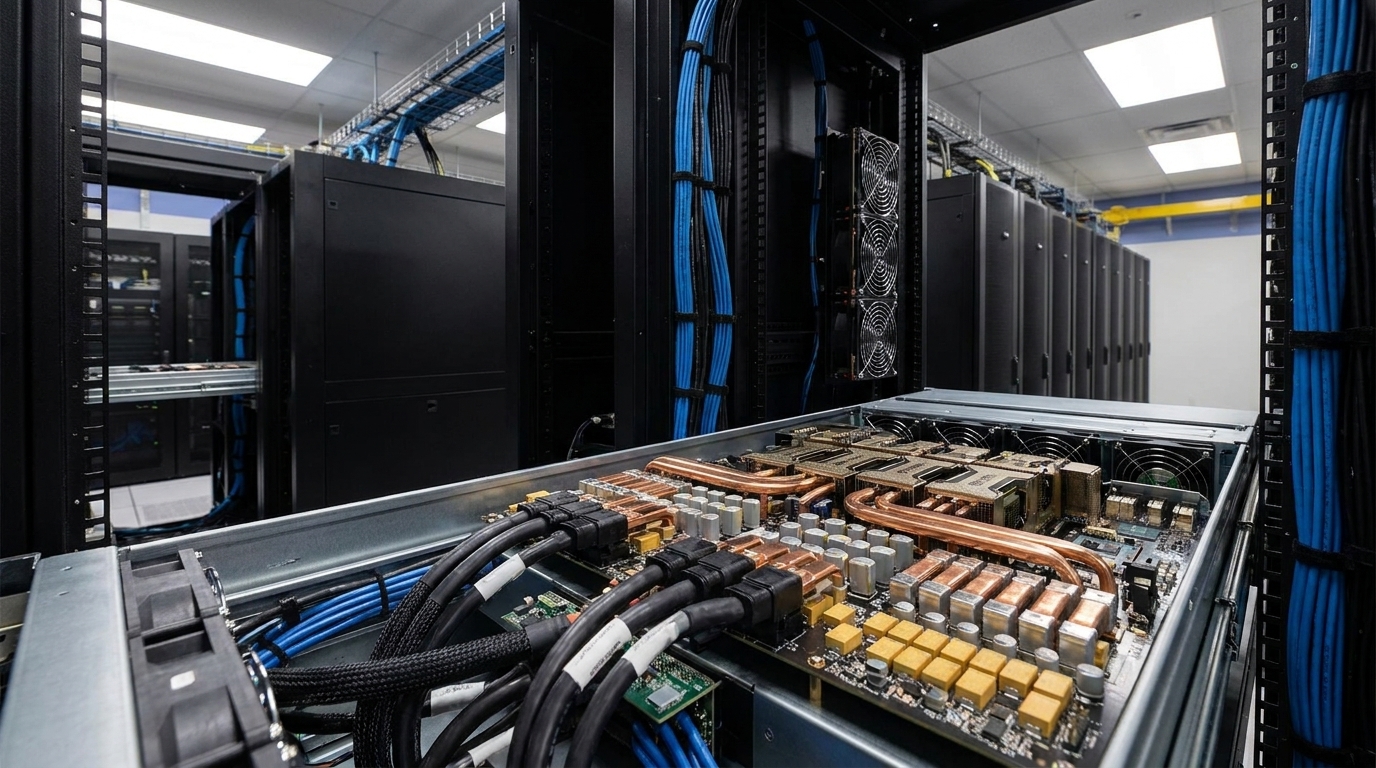 MLCC vs Polymer Tantalum Capacitors: Overcoming 2026 Shortages in AI Server PDNsUTMEL07 August 2026683
Facing 2026 MLCC lead times of up to 24 weeks driven by AI server demand, hardware engineers are substituting multi-layer ceramic capacitors with conductive polymer tantalum capacitors. While Class II MLCCs suffer severe DC bias capacitance loss and acoustic noise, polymer tantalums offer voltage stability and low ESR. Implementing a division-of-labor strategy—using polymer tantalums for bulk decoupling and MLCCs for point-of-load—optimizes PDN performance and bypasses supply bottlenecks.
Read More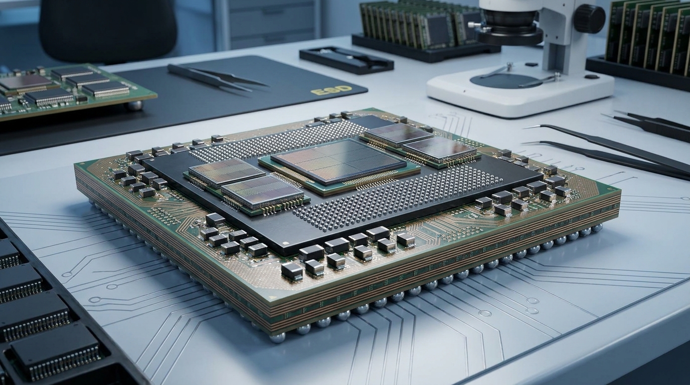 Sourcing Silicon Capacitors and MLCCs in the AI Hardware EraUTMEL13 August 2026597
Modern AI hardware requires a hybrid Power Delivery Network (PDN) to maintain low-voltage stability under extreme transient currents. Deep Trench Silicon Capacitors (DTCs) integrate directly into advanced packages to deliver ultra-low ESL and stable performance for high-frequency transient suppression. Meanwhile, Multilayer Ceramic Capacitors (MLCCs) provide essential bulk energy storage on the motherboard, making both technologies complementary across the AI power stack.
Read More MLCC DC Bias Derating: How to Calculate and Compare Effective Capacitance Before Component SelectionUTMEL11 September 2026566
Class II ceramic capacitors suffer significant capacitance loss under DC voltage due to ferroelectric domain saturation and high electric field intensity. This comprehensive engineering guide explains how to calculate true worst-case effective capacitance by compounding DC bias, temperature, tolerance, and aging. It provides multi-vendor simulation workflows, benchtop impedance measurement techniques, and practical guidelines to maintain power supply stability and avoid costly design failures.
Read More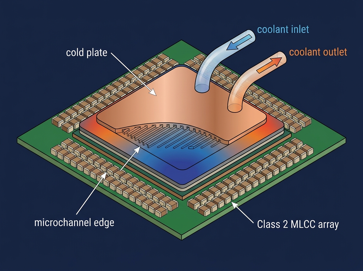 Thermal Management in AI Servers: Specifying Class 2 MLCCs (X7R/X7S) for Liquid Cooling EnvironmentsUTMEL13 July 2026373
Explore how the transition from traditional air-cooling to liquid cooling (direct-to-chip and immersion) in high-density AI server racks alters component thermal profiles. Focus on why design engineers are increasingly specifying Class 2 MLCCs (X7R and X7S dielectrics) over standard X5R variants to prevent thermal degradation near the liquid cooling microchannels. Explain how these capacitors mitigate acoustic noise and voltage bias degradation under heavy workloads. Provide sourcing advice for high-reliability passives via UTMEL during this high-demand memory and passive component super-cycle.
Read More
Subscribe to Utmel !
![SMPA-144FG-ACTEL-1]() SMPA-144FG-ACTEL-1
SMPA-144FG-ACTEL-1Microchip
![SM208PQ-ACTEL-3]() SM208PQ-ACTEL-3
SM208PQ-ACTEL-3Microchip
![ZLR962282H]() ZLR962282H
ZLR962282HMicrochip
![IPR-DDR3/UNI]() IPR-DDR3/UNI
IPR-DDR3/UNIIntel
![IPR-RSCODECII]() IPR-RSCODECII
IPR-RSCODECIIIntel
![SP365002918UTJ]() SP365002918UTJ
SP365002918UTJInfineon
![26603]() 26603
26603Lapp
![MAX32010EVKIT#]() MAX32010EVKIT#
MAX32010EVKIT#Maxim
![MAX32680EVKIT#]() MAX32680EVKIT#
MAX32680EVKIT#Maxim
![DC1429A]() DC1429A
DC1429AAnalog Devices
