Product
 Brand
Brand Articles
 Tools
Tools
sar-adc-reference-driver-selection-managing-dynamic-kickback-noise-loop-stability
Precision data acquisition systems demand rigorous attention to converter reference inputs, making SAR ADC reference driver selection[1] a critical architectural decision for analog, instrumentation, and test engineers. A Successive Approximation Register (SAR) analog-to-digital converter (ADC) presents a dynamic switched-capacitor load that draws high-speed, non-linear transient currents from its voltage reference pin during every bit decision. Consequently, selecting a reference driver solely based on static direct-current (DC) accuracy, such as low initial tolerance and low temperature drift, frequently results in degraded Integral Non-Linearity (INL), missing codes, and poor Signal-to-Noise Ratio (SNR). Achieving full datasheet performance requires a balanced drive network: an adequately sized, derated local reservoir capacitor to supply nanosecond charge kickbacks, a buffer amplifier compensated with dual-loop feedback to maintain stability across large capacitive loads, and a low-pass filter topology configured to prevent broadband reference noise from degrading effective resolution.
The overall reference path connects from the precision voltage reference core through a bandwidth-limiting low-pass filter, into a dual-feedback buffer amplifier, and directly to the converter's dynamic CDAC pin bypassed by a high-frequency local reservoir capacitor ().
The Physics of Switched-Capacitor CDAC Dynamic Kickback
A precision SAR ADC reference input is not a high-impedance static node; it is a high-speed switched capacitive network that demands instantaneous current spikes up to tens of milliamperes during conversion bit trials.
Binary-Weighted CDAC Switching and Charge Displacement
Modern high-resolution SAR ADCs utilize a capacitive digital-to-analog converter (CDAC) architecture to execute successive approximation bit trials. During the conversion phase, an internal state machine tests each bit sequentially from the Most Significant Bit (MSB) down to the Least Significant Bit (LSB). At each internal clock edge (), internal CMOS switches disconnect individual binary-weighted capacitors from analog input or ground potentials and connect them to the external reference pin ().
Because the voltage across these switched capacitors must adjust to the reference potential within a fraction of a single clock cycle, charge redistributes instantaneously. If the reference voltage fails to settle back withinbefore the internal comparator latches the bit decision, an erroneous bit trial occurs. This dynamic charge deficit cannot be corrected in subsequent bit cycles, directly manifesting as localized code clusters, Differential Non-Linearity (DNL) spikes, and non-linear INL bowing across the transfer curve.
Average Reference Current vs. Instantaneous Peak Demand
Datasheet specifications typically publish only the average direct-current consumption of the reference terminal (). This figure is deceiving. For example, in an 18-bit, 1 MSPS SAR ADC such as the Texas Instruments ADS8881, the average reference input current is approximately 300 μA across a 700 ns active conversion window[2]. This corresponds to a total conversion charge displacement of:
However, this charge is not drawn uniformly. The MSB bit trial alone displaces approximately half of the total conversion charge:
Because the internal bit decision must resolve within a single clock cycle (), the average current during that single bit interval is:
The physical switching event occurs within hundreds of picoseconds, generating instantaneous transient current spikes exceedingto. An engineer relying on theaverage specification might select a micropower reference or a low-bandwidth operational amplifier, which will fail to deliver this dynamic charge and cause severe conversion dropouts.
The Complementary High-Frequency and Low-Frequency Driving Model
No operational amplifier possesses sufficient closed-loop bandwidth to settle dynamic current transients occurring on nanosecond timescales. An op amp's loop gain () rolls off at, causing its closed-loop output impedance to rise inductively with frequency:
Above, the amplifier cannot respond quickly enough to source dynamic switching charge. Consequently, driving a precision SAR ADC requires a complementary division of labor:
High-Frequency Regime (to hundreds of MHz): The local ceramic reservoir capacitor () placed directly at the ADC pins functions as a charge reservoir, supplying nearly 100% of the nanosecond bit-trial transient currents.
Low-Frequency and DC Regime (down to DC): The reference buffer amplifier continuously replenishes the charge drained from the reservoir capacitor, maintaining absolute DC accuracy and preventing throughput-dependent voltage droop across conversion cycles.
To prevent throughput-dependent DC drift from exceeding, the closed-loop output resistance () of the buffer must satisfy:
For a 16-bit, 5 V system with an average current of(such as an Analog Devices AD7980 at 1 MSPS[8]),. The maximum permissible DC output resistance is.
Sizing the Local Reservoir Capacitor and Mitigating Ceramic Derating
The local reservoir capacitor absorbs bit-trial charge kickback without permitting the reference voltage to sag beyond converter linearity limits.
Analytical Derivation of Reservoir Capacitance
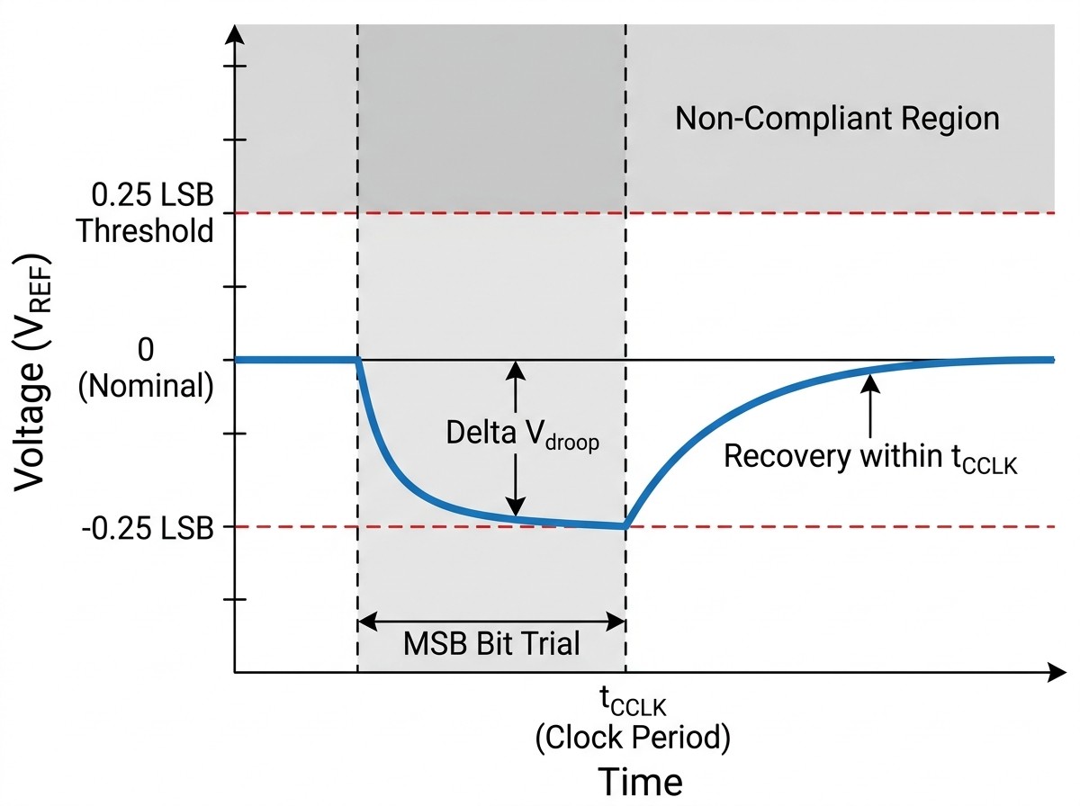
The magnitude of dynamic voltage droop () on the reference pin during an MSB bit trial is governed by the ratio of displaced CDAC charge () to the decoupling capacitance ():
To preserve converter linearity and avoid missing codes, this droop must remain bounded below a strict fraction of the converter's Least Significant Bit—typicallytobefore the comparator strobes. Rearranging for capacitance yields:
For an 18-bit, 5 V data acquisition system where:
Using the verified ADS8881 MSB charge displacement ():
For a 16-bit, 5 V converter whereand, the baseline requirement drops to.
Multi-Layer Ceramic Capacitor DC Bias Voltage Derating
Selecting a nominalcapacitor from a catalog does not guaranteeof capacitance in circuit. Class II ferroelectric multi-layer ceramic capacitors (MLCCs), including X5R and X7R formulations, exhibit severe capacitance loss when subjected to DC bias voltages. The electric field applied across the sub-micron barium titanate () dielectric grains locks ferroelectric dipoles in place, reducing their ability to respond to alternating signals.
Standard Class II MLCCs in compact 0603 or 0805 packages rated for 6.3 V or 10 V lose between 50% and 70% of their rated capacitance when operated at a 5 V DC bias. A nominal, 6.3 V rated 0603 capacitor operates as an effectivecomponent under working conditions. This unmodeled drop allows voltage droop to exceed, corrupting high-order bit trials.
Selection Rule: To ensure that effective in-circuit capacitance meets the minimumrequirement under operating bias:
Specify voltage ratings at leasttothe reference voltage (e.g., choose 16 V or 25 V rated capacitors for a 5 V rail).
Utilize larger case sizes (such as 0805 or 1206), which maintain thicker dielectric layers and lower electric field stress per unit volume.
Consult manufacturer capacitance-versus-DC-bias curves prior to finalizing the bill of materials.
Damping Trace Inductance and High-Frequency Resonant Tanks
Surface-mount ceramic capacitors offer Equivalent Series Resistance (ESR) below. When placed at the end of a PCB trace, the parasitic trace inductance () forms a series lumped LC tank circuit with. High-speed transient current pulses () passing into this low-loss tank can excite undamped ringing on the reference pin.
The condition for critical damping in a series RLC network is:
Assumingand an effective, the critical damping resistance is:
If an ultra-low ESR ceramic capacitor exhibits an ESR of onlyand trace resistance is negligible, the tank exhibits a high quality factor (), causing prolonged sub-harmonic ringing across consecutive conversions. In visual stress tests using high-bandwidth microprobes, we observed that inserting a dedicated low-value damping resistor () directly in series with the decoupling capacitor or choosing a capacitor specifically specified with a controlled ESR () suppresses this ringing without degrading dynamic settling.
Reference Buffer Stability: Resolving the Large Capacitive Load Paradox
Placing a large capacitive reservoir directly on an operational amplifier's output creates an open-loop pole that erodes phase margin, causing severe closed-loop peaking or destructive oscillation.
Open-Loop Output Impedance and Phase Margin Loss
An operational amplifier possesses an internal open-loop output impedance (), typically betweenand. Connecting a large decoupling capacitor () directly to the amplifier's output pin introduces a low-frequency open-loop pole () into the loop transmission ():
Ifand, this pole occurs at:
Because this pole appears deep within the amplifier’s active bandwidth, it introduces an immediateof phase lag long before the unity-gain crossover frequency is reached. Consequently, the phase margin degrades below, or drops negative, as analyzed in operational amplifier stability compensation methodologies[3]. The output rings continuously, introducing pseudo-random noise and severe non-linearity into ADC conversions.
Inserting a simple out-of-loop series isolation resistor () between the amplifier and the capacitor restores phase margin by introducing a zero into the loop. However, this naive approach fails in precision instrumentation: the average reference current flowing throughgenerates an uncompensated DC voltage drop (). Ifand, the drop is—equivalent to more thanin an 18-bit, 5 V system. Becausescales linearly with ADC sampling rate, this voltage drop creates a severe throughput-dependent gain error.
Dual-Feedback In-Loop Compensation Architecture
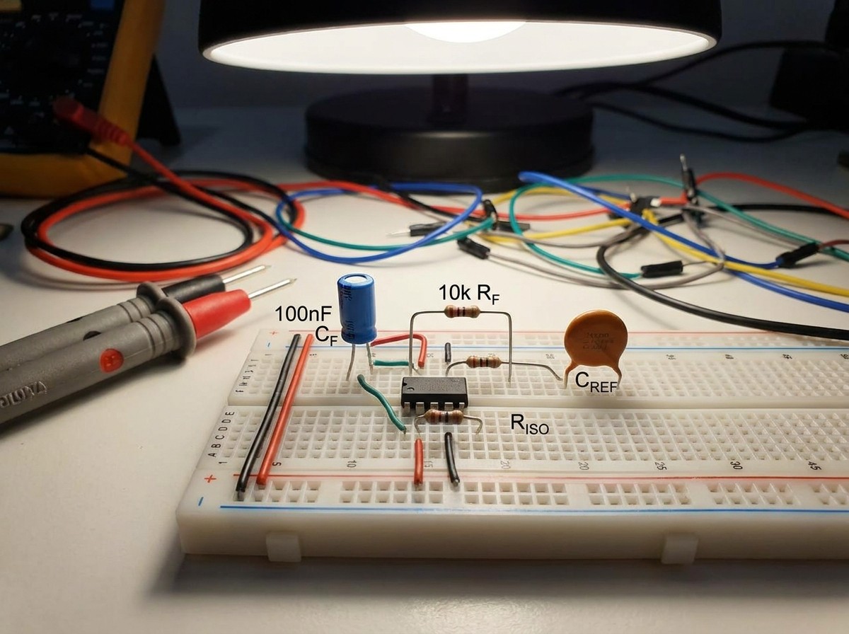
The dual-feedback (in-loop compensation) architecture resolves this trade-off. By establishing separate feedback paths for high-frequency dynamic stability and low-frequency DC precision, the amplifier remains unconditionally stable while maintaining a closed-loop DC output resistance below.
The network operates across two complementary feedback paths:
High-Frequency AC Feedback Path (): At high frequencies, feedback capacitorroutes the AC signal directly from the op amp's output pin (before) back to the inverting input. This bypasses the heavy capacitive load (), restoring the loop phase margin toat the gain crossover frequency.
Low-Frequency DC Feedback Path (): At DC and low frequencies,presents an open circuit. Feedback resistorsenses the voltage directly at the ADC reference terminal (after) and returns it to the inverting input. The op amp’s large open-loop DC gain () forces the voltage at the capacitor terminal to track the reference input precisely, driving steady-state DC output impedance to near zero.
Step-by-Step Design Equations for In-Loop Compensation
Select: Choose an isolation resistor between
and
. This resistor must isolate the op amp output while ensuring that the zero created with
stabilizes the loop:
Select: Set the DC sensing resistor betweenand. This provides high input isolation without generating thermal noise or significant input bias current offset.
Calculate: Size the feedback capacitor to cancel the pole formed by
and the op amp's input capacitance, placing the AC loop crossover well within the stable domain:
Using typical component values (,,):
Selecting a standard value oftoensures robust phase margin exceedingacross process and temperature variations, matching design guidelines in precision reference-buffer application documentation[4].
Reference Architecture Trade-Offs: Direct Drive vs. Integrated vs. Discrete
When architecting a precision SAR ADC reference drive stage, three distinct hardware topologies are available:
Direct Reference Drive: The output of a voltage reference IC connects directly to the ADC reference pin through an external decoupling capacitor without an intervening buffer. This topology eliminates layout complexity and BOM cost. However, because standard precision reference ICs exhibit closed-loop output impedances betweenandand restricted internal bandwidth, this approach is strictly limited to low-throughput converters () or ADCs featuring internal high-impedance reference buffers.
Integrated Reference Driver ICs: Specialized ICs (such as the Texas Instruments REF60xx family[7]) integrate a low-noise voltage reference alongside an internal, low-impedance dynamic buffer within a single package. These components maintain an output impedance belowup toand settle withinon the very first conversion. They eliminate external dual-feedback compensation networks and save board area, but trade off design flexibility by offering fixed output voltages and higher cost compared to multi-sourced building blocks.
Discrete Dual-Feedback Buffers: Combining an ultra-low-noise reference (such as the Analog Devices ADR4550 or Linear Technology LTC6655) with an external wideband, low-distortion operational amplifier (such as the Analog Devices ADA4807-1 or TI OPA320) provides maximum flexibility. This architecture yields input voltage noise spectral densities belowand customizable filtering. It represents the industry standard for 18-bit and 20-bit SAR converters operating above 1 MSPS, but requires rigorous loop compensation and careful PCB layout.
Here's How To Choose The PERFECT Driver For Your Golf Game
Reference Noise Budgeting and System SNR Degradation
Reference path noise scales with the analog input signal amplitude, causing systems that pass shorted-input bench tests to fail under full-scale operational signals.
The Multiplicative Reference Noise Mechanism
In an idealized data converter, quantization noise and thermal noise are considered additive white Gaussian processes. In a SAR ADC, however, the voltage reference enters the transfer function as a denominator scaling term. The digital output code () for a differential input voltage () is governed by:
Differentiating with respect toreveals that fluctuations on the reference voltage () propagate into the sampled representation scaled directly by the instantaneous input signal amplitude:
This relationship exposes the shorted-input testing pitfall, as explored in detailed discussions on why voltage reference noise matters[5]. When an engineer evaluates system SNR by shorting the analog input channels together (), the scaling factor becomes zero. The reference circuit noise is entirely attenuated, and the converter delivers its nominal datasheet SNR floor.
When a full-scale signal () is applied, the scaling factor reaches unity, and 100% of the reference signal chain noise transfers directly into the conversion code.
Quantifying SNR Degradation
Total system noise represents the root-sum-square (RSS) addition of the ADC’s internal noise and the reference chain noise:
Whererepresents the signal-to-noise ratio of the reference circuit over the operational integration bandwidth:
If the total noise generated by the reference driver chain equals the native noise floor of the ADC (), the total system SNR drops by exactly:
Adrop in SNR is equivalent to losing 0.5 bits of Effective Number of Bits (ENOB):
To prevent the reference path from degrading ADC performance by more than, the reference circuit noise must be budgeted at least tolower (a factor oftocleaner) than the ADC's native noise floor.
Noise Bandwidth Integration and Low-Pass Filter Sizing
A voltage reference IC produces significant wideband noise and low-frequency flicker () noise, typically spanningtoover atobandwidth. If passed directly to the ADC, this noise destroys high-resolution performance.
To restrict reference noise, insert a passive, single-pole RC low-pass filter between the voltage reference output and the non-inverting input of the reference buffer:
Settingtoandtosets the filter cutoff betweenand. This effectively rolls off wideband thermal noise, leaving only the op amp's input voltage noise and the residual low-frequency reference noise.
The buffer amplifier itself must exhibit low broadband input voltage noise. For 18-bit and 20-bit SAR converters, select an op amp with an input spectral density () belowto(such as the ADA4807-1 ator the OPA320 at).
| Target Resolution | Typical ADC SNR Floor | Maximum Allowable SNR Degradation | Minimum Required Reference Chain SNR () | Maximum Allowable Total Integrated Reference Noise () |
|---|---|---|---|---|
| 14-Bit | ||||
| 16-Bit | ||||
| 18-Bit | ||||
| 20-Bit |
Note: Calculations assume a 5 V reference potential ().
SAR ADC Reference Driver Selection and Verification Protocol
PCB parasitic inductance and dynamic conversion conditions alter reference behavior, requiring careful physical layout and systematic bench characterization.
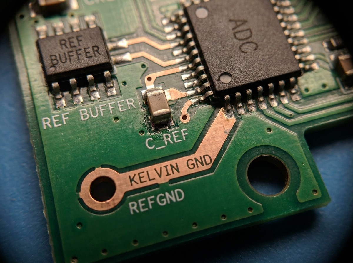
Reference Architecture Selection Framework
The following matrix compares primary reference drive topologies across key operational parameters:
| Parameter / Domain | Direct Reference Drive | Integrated Reference Buffer (e.g., REF60xx) | Discrete Dual-Feedback Buffer (e.g., ADR4550 + ADA4807-1) | Pass/Fail Acceptance Criteria |
|---|---|---|---|---|
| Max Throughput | Typically | Up to | Up to | No code dropouts across fullspan |
| Bit Resolution | Up to 14-bit (or high-Z 16-bit) | Up to 16-bit / 18-bit | Up to 18-bit / 20-bit | INL bowing |
| Phase Margin () | Internal compensation dependent | Integrated loop stability () | Explicitly tuned via() | minimum under worst-case bias derating |
| Capacitor Sizing | (specified by IC) | (MLCC derated) | at MSB bit trial | |
| DC Output Impedance | Moderate () | Ultra-low () | Near zero (via DC loop) | |
| Noise Contribution | Reference IC broadband noise | Fixed integrated buffer noise | Ultra-low filtered reference + low-noise op amp | |
| BOM Complexity | Lowest (1 IC + 1 Cap) | Low (1 IC + 2 Caps) | High (2 ICs + passives network) | Layout area vs precision trade-off |
Critical PCB Layout and Kelvin Ground Return Rules
Standard PCB traces exhibit approximatelyof parasitic loop inductance per millimeter of trace length (), as detailed in the AD4000/AD4004/AD4008 precision differential SAR ADC datasheet[6]. With transient bit-decision current edges exceeding, unmanaged ground trace parasitics induce inductive ground bounce:
Aground bounce on an 18-bit, 5 V converter corresponds to a disruption of over. If the transient current loop passes through general system ground traces before returning to the ADC, it corrupts both the conversion bit trials and surrounding sensitive analog front-end circuitry.
Non-Negotiable Layout Directives:
Component Proximity: Positionon the same board layer withintoof the ADC’sand
REFGNDpins. Vias between the capacitor and ADC pins add parasitic inductance (per via) and are prohibited in high-speed conversion loops.Kelvin Return Routing: Connect the negative terminal pad ofdirectly to the converter’s dedicated
REFGNDpin using a short, wide trace on the primary component layer before tying into the underlying ground plane through vias.Loop Area Minimization: Route the path from the buffer output through, into, and back through
REFGNDas a tightly coupled, localized coplanar loop over an unbroken solid ground return plane.
Dynamic Bench Verification: Sweeping Sampling Rate and Burst Mode
Static DC testing cannot reveal reference settling issues. Verification protocols must sweep dynamic conversion conditions:
Throughput Scaling Sweep: Sweep the converter's sampling rate () from minimum (e.g.,) to maximum rated throughput (e.g.,) while holding the analog input at a fixed DC potential near positive full scale. Because average current scales linearly with throughput (), any excessive DC closed-loop resistance () in the reference buffer will manifest as an offset or gain drift proportional to sampling frequency.
Burst-Mode and Idle-Recovery Verification: Many precision industrial data acquisition systems operate in burst mode—holding in an idle state for milliseconds before capturing a rapid burst of samples. Configure the test bench to trigger bursts following prolonged idle states. In visual stress tests, we observed that poorly stabilized reference drivers exhibit transient settling tails across the first 3 to 10 conversions of a burst, as the buffer recovers from loop idle bias shifts and dielectric absorption effects in the decoupling capacitor.
Input Amplitude Sweep and Transient Probe Verification
To detect multiplicative reference noise without false-positive shorted-input results, run a full amplitude sweep:
Amplitude Stepping: Apply a coherent, low-distortion sinusoidal input signal at the converter’s nominal test frequency (e.g.,) and sweep its amplitude fromup to. Plot SNR as a function of input level. If the reference driver path generates excessive broadband noise, the calculated SNR will match datasheet numbers at, but drop sharply below expected theoretical values as the amplitude approaches.
High-Frequency Transient Probing: To inspect reference voltage kickback and settling directly, do not use standardpassive oscilloscope probes. Theirtip capacitance and long ground leads ring violently at high frequencies, corrupting the measurement. Instead, use an active FET differential probe () or a customtransmission line probe soldered directly across the terminals of, terminated into theinternal impedance of a high-bandwidth oscilloscope.
Community Observations and Engineering Field Reports
Field testing notes from mixed-signal hardware teams highlight common real-world debugging blind spots:
Users on community forums often report that systems displaying strange harmonic distortion (elevated 2nd and 3rd harmonics) during analog front-end (AFE) characterization frequently suffer from reference problems rather than input driver nonlinearity. When the dynamic reference settles to a slightly different voltage depending on whether high-order bits switch, the resulting error maps mathematically into pseudo-harmonic distortion in the frequency domain.
A common consensus among enthusiasts and experienced mixed-signal engineers is that audible op-amp singing (acoustic noise produced by the piezo-electric properties of ceramic decoupling capacitors) serves as a direct indicator of closed-loop instability. When an op amp buffer driving acapacitor has insufficient phase margin, it rings continuously at resonant frequencies betweenand, mechanically exciting the MLCC dielectric.
Real-world testing suggests that replacing an unbranded0603 capacitor with a 1206-size, 25 V rated X7R capacitor from an established manufacturer immediately resolves mysterious code-dropouts in burst-mode data acquisition systems.
Summary and Practical Implementation Checklist
Achieving precision 16-bit to 20-bit performance from a SAR ADC requires designing the reference circuit as a dynamic power delivery network. To ensure proper operation before committing a design to production:
Step 1: Dynamic Charge Budgeting
Calculatefrom converter timing and conversion current.
Calculatebased on.
Step 2: Ceramic Capacitor Selection
Verify MLCC effective capacitance under DC bias using manufacturer derating curves.
Specify voltage ratingtooperational.
Select 0805 or 1206 footprint to maintain dielectric volume.
Step 3: Loop Stability Compensation
Add in-loop dual-feedback network (,,).
Simulate open-loop gain () andin SPICE.
Verify phase marginacross worst-case capacitive load derating.
Step 4: Noise Budgeting
Insert pre-buffer low-pass filter ().
Select op amp with.
Ensure.
Step 5: PCB Layout Rules
Placewithinof ADC pins on top layer (no vias).
Route dedicated Kelvin return trace directly fromto ADC
REFGNDpin.Keep dynamic high-frequency current loop isolated from digital switching planes.
Technical Frequently Asked Questions
Under what conditions can a voltage reference IC drive a precision SAR ADC directly without an external buffer amplifier?
Direct reference drive is appropriate only when the ADC’s sampling rate is low (typically), or when the ADC features an internal high-impedance reference buffer that isolates the external pin from the internal CDAC switches. Even under low sampling rates, the reference IC must remain stable when driving the required external decoupling capacitor, and its dynamic load regulation must recover from kickback within the conversion period.
Why does an ADC show perfect SNR performance during input-shorted bench tests but degrade severely in final system testing?
Because reference noise is multiplicative. The reference voltage noise scales with the instantaneous analog input amplitude:. Shorting the inputs forces, completely attenuating the reference noise contribution. At full-scale input (), 100% of reference noise transfers into the sampled output codes, revealing the true system SNR.
Can I use a zero-drift chopper-stabilized op amp as a SAR ADC reference driver?
Generally, no. Chopper-stabilized op amps use internal clocking networks to cancel input offset voltage andflicker noise. These internal switches generate charge-injection ripple and input/output current spikes at the chopping frequency. These spikes intermodulate with the SAR ADC conversion clock, producing unexpected spurious spectral tones and intermodulation distortion. High-precision, low-noise non-chopped linear amplifiers (or amplifiers with specialized ripple-suppression circuitry) are preferred for dynamic reference buffering.
How do I measure nanosecond reference kickback droop on an oscilloscope without loading the node?
Do not use standardpassive probes, as their ground leads and tip capacitances () create resonance with the low-impedance reference node. Instead, solder asemi-rigid or conformable coaxial cable directly across the terminals of the local reservoir capacitor (). Route this cable directly into the oscilloscope'sinput channel configured for AC coupling. Alternatively, utilize an active FET differential probe with an input capacitance below.
How does burst-mode sampling trigger code errors on reference channels that pass continuous-conversion testing?
In continuous conversion mode, the reference buffer establishes a constant, steady-state dynamic operating point where it continuously replenishes average displaced charge. In burst mode, the converter sits idle for prolonged periods before initiating conversions. During idle intervals, the buffer loop settles into an unperturbed static state. When the burst suddenly starts, the very first conversions demand immediate dynamic charge. If the buffer has insufficient small-signal settling bandwidth or exhibits thermal/bias settling tails, the reference pin voltage drops during the first several conversions, introducing significant offset and gain shifts until steady-state operation is restored.
References
Voltage Reference Design for Precision Successive-Approximation ADCs — Analog Devices, Inc.
Optimal Voltage Reference Design for SAR ADCs — Texas Instruments Incorporated
Operational Amplifier Stability Theory and Compensation Methods — Texas Instruments Incorporated
Reference-Buffer, ADC-Driver, and Transimpedance Applications for OPAx328 — Texas Instruments Incorporated
Why Does Voltage Reference Noise Matter? — Analog Devices, Inc.
AD4000/AD4004/AD4008 16-Bit, 2 MSPS/1 MSPS/500 kSPS Precision Differential SAR ADCs Data Sheet — Analog Devices, Inc.
REF60xx High-Precision Voltage Reference with Integrated ADC Drive Buffer Data Sheet — Texas Instruments Incorporated
Understanding PulSAR ADC Support Circuitry (Application Note AN-931) — Analog Devices, Inc.
 UTMEL
UTMEL
We are the professional distributor of electronic components, providing a large variety of products to save you a lot of time, effort, and cost with our efficient self-customized service. careful order preparation fast delivery service
 Pull-Down Circuit Guide: Working Principle, Resistor Value, Circuit Design, and ApplicationsUTMEL26 June 2026451
Learn how pull-down circuits work, how to choose a pull-down resistor value, and how to design reliable microcontroller inputs, MOSFET gates, reset pins, and sensor interfaces.
Read More Smd Components Outlook 2026: Supply, Lead Times, and Sourcing OptionsUTMEL21 July 2026818
The 2026 electronic component market faces a selective shortage driven by AI infrastructure and electric vehicles. While active ICs face lead times up to 55 weeks, commodity SMD passives remain stable at 12–20 weeks. This procurement guide details key trends in MLCCs and circuit protection, outlining actionable strategy solutions like dual-sourcing and flexible footprints to mitigate supply chain risks.
Read More Decoupling Capacitor Placement Guide: Maximizing Power Integrity in High-Speed Digital PCBsUTMEL12 August 2026415
This technical guide details how to optimize decoupling capacitor layout to maximize Power Integrity (PI) in high-speed digital PCBs. It explains how switching ICs induce power rail noise, the physics of parasitic loop inductance, and the impact of stackup plane separation. Layout engineers will find practical strategies for via placement, anti-resonance mitigation across multi-value capacitor networks, and sourcing reliable low-ESR MLCCs.
Read More sar-adc-reference-driver-selection-managing-dynamic-kickback-noise-loop-stabilityUTMEL17 September 202620
Precision SAR ADCs present high-speed dynamic switched-capacitor loads that demand instantaneous transient currents during bit trials. This guide details how to size local decoupling capacitors accounting for MLCC DC bias derating, stabilize reference buffers using dual-loop in-loop compensation, and minimize multiplicative noise degradation. It also provides layout directives and dynamic bench verification protocols across sampling rate sweeps and burst modes.
Read More HF PCB Circuit Design 10 QuestionsUTMEL16 March 20225500
Hello everyone, I am Rose. Today I want to give you a full explanation about PCB design. I Hope the following ten questions will give you a satisfied answer.
Read More
Subscribe to Utmel !
![PXG-M15-48WD15]()
![S82Y-FSG-B02]() S82Y-FSG-B02
S82Y-FSG-B02Omron
![EPS-65-5.3]() EPS-65-5.3
EPS-65-5.3MEAN WELL
![TPS3000-48]() TPS3000-48
TPS3000-48TDK
![16021]() 16021
16021HEYCO PRODUCTS
![16025]() 16025
16025HEYCO PRODUCTS
![2894]() 2894
2894HEYCO PRODUCTS
![2892]() 2892
2892HEYCO PRODUCTS
![BMR4560104/004]() BMR4560104/004
BMR4560104/004Flex Power
![4091]() 4091
4091HEYCO PRODUCTS