Product
 Brand
Brand Articles
 Tools
Tools
Decoupling Capacitor Placement Guide: Maximizing Power Integrity in High-Speed Digital PCBs
Executive Summary & Decision Framework
The fundamental rule of decoupling capacitor layout is not about accumulating raw capacitance—it is about minimizing total parasitic loop inductance (Lloop). If the power and ground planes on your multilayer board are separated by 10 mils or less, high-frequency decoupling effectiveness becomes largely independent of physical distance across the plane pair. If you are routing surface traces to leaded packages or working with two-layer boards, physical proximity to the IC pin remains critical. This guide breaks down the physics, the layout strategies, and the component selection rules that senior SI/PI engineers apply to achieve robust Power Integrity (PI) in high-speed digital PCBs.
What is Power Integrity (PI) and Why Do Decoupling Capacitors Matter?
Modern high-speed ICs—FPGAs, SoCs, and DDR memory controllers—switch logic states in picoseconds. Each transition demands an instantaneous current surge (di/dt) from the Power Distribution Network (PDN). Because the PDN possesses parasitic inductance, that transient current generates a voltage disturbance governed by Faraday’s Law of Induction[2]:
Vdroop = LPDN · (di / dt)
The result is a momentary collapse of the power rail (voltage droop) and a local shift in the ground reference potential (ground bounce). The voltage regulator module (VRM) cannot respond to these sub-nanosecond events because its control loop bandwidth is typically limited to the kilohertz range. Decoupling capacitors solve this problem by acting as local high-speed energy reservoirs—they supply instantaneous charge directly to the switching transistors, holding the rail voltage within tolerance until the VRM catches up.
To maintain power integrity across the full operating bandwidth (DC to multi-GHz), the PDN impedance must stay below a target threshold[1] defined by the IC’s supply voltage tolerance and transient current demand:
Ztarget = ΔVallowed / ΔItransient
Every decoupling capacitor placed on your board, and every millimeter of trace connecting it, either contributes to or undermines this impedance budget.
The Core Enemy: Minimizing Parasitic Loop Inductance
The single most important metric in decoupling capacitor layout is total loop inductance. Current always flows in a closed loop: from the IC power pin, through the decoupling capacitor, and back to the IC ground reference. The physical area enclosed by this loop determines the inductance (L ≈ Φ / I), and that inductance directly limits how fast the capacitor can deliver charge.
Total loop inductance has three components:
Ltotal = LESL + Lmounting + Ltrace/plane
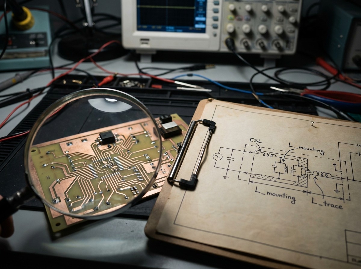
LESL is the internal Equivalent Series Inductance of the capacitor package.
Lmounting is the inductance introduced by pads, trace stubs, and vias.
Ltrace/plane is the inductance of the path through surface traces or internal planes.
Decoupling Package & ESL Comparison
| Package Size | Typical ESL Range (nH) | Typical Mounting Inductance (nH) | Recommended Frequency Band | Primary Application |
|---|---|---|---|---|
| 0201 | ~0.2–0.4 | ~0.3–0.5 (via-in-pad) | >200 MHz | GHz-range local decoupling |
| 0402 | ~0.4–0.8 | ~0.5–1.0 | 50–200 MHz | Mid-band decoupling |
| 0603 | ~0.8–1.5 | ~1.0–2.0 | <50 MHz | Bulk / low-speed decoupling |
| 0805 | ~1.2–2.0 | ~1.5–3.0 | <20 MHz | Bulk capacitors |
| 0204/0306 (Reverse Geometry) | ~0.28–0.35 | ~0.3–0.5 | >200 MHz | High-performance local decoupling |
Smaller packages typically exhibit lower ESL because current travels a shorter distance through the internal electrode structure. Reverse-geometry capacitors (0306 or 0204) take this further by rotating the internal electrodes 90 degrees, shortening the current path within the package itself.
The 30-Year Proximity Myth: Surface Traces vs. Internal Power Planes
One of the most persistent application note boilerplates states: “Place decoupling capacitors as close as possible to the IC power pin.” For multilayer boards with closely spaced internal power and ground planes, research conducted by Dr. Todd Hubing and published in IEEE literature has demonstrated that this one-size-fits-all rule is incomplete, and in some geometries, misleading.
Scenario A: Surface Trace Routing (Quad Flat Packs & Edge-Disposed Leads)
When a capacitor connects to an IC via surface traces, the trace inductance is substantial—typically 5 to 7 nH per inch. Under these conditions, every millimeter of distance adds parasitic inductance, progressively degrading high-frequency decoupling performance. For leaded packages and two-layer boards, placing capacitors within a few millimeters of the power pin is mandatory.
Scenario B: Internal Power/Ground Planes (BGAs & Multilayer PCBs)
High-speed ICs packaged in Ball Grid Arrays (BGAs) route power and ground through vias that drop directly into internal planes. These internal plane pairs—when separated by 10 mils or less of dielectric—exhibit a phenomenon called spreading inductance. Spreading inductance is measured in pH per square (inductance per unit geometry) and is typically around 100 pH per square for a 4-mil dielectric.
On a typical board, moving a decoupling capacitor an entire inch across a closely spaced plane pair adds approximately 0.1 to 0.25 nH of spreading inductance. Compare this to the ~3 nH of total mounting inductance (capacitor ESL plus via inductance): the added inductance from distance across the plane is mathematically negligible. Dr. Hubing’s 1995 IEEE impedance curves visually prove this—four different capacitor locations on a multilayer board produce nearly identical high-frequency PDN impedance profiles.
Does Decoupling Capacitor Placement Actually Matter?
The Critical 10-Mil Caveat
This “location-independent” decoupling behavior holds only when power and ground planes are separated by 10 mils or less. If your stackup spaces planes far apart (>10 mils), if you are working with a two-layer board without solid internal planes, or if you route decoupling capacitors through surface traces rather than directly into plane pairs, physical proximity to the IC pin remains critical. Proper power plane segmentation and decoupling capacitor placement[5] strategies must be implemented for sparse or thick stackups.
Capacitor Layout and Via Routing Strategies
Once you select the right components, how you route the connections dictates whether those capacitors deliver their rated performance.
Via Placement Hierarchy (Best to Worst)
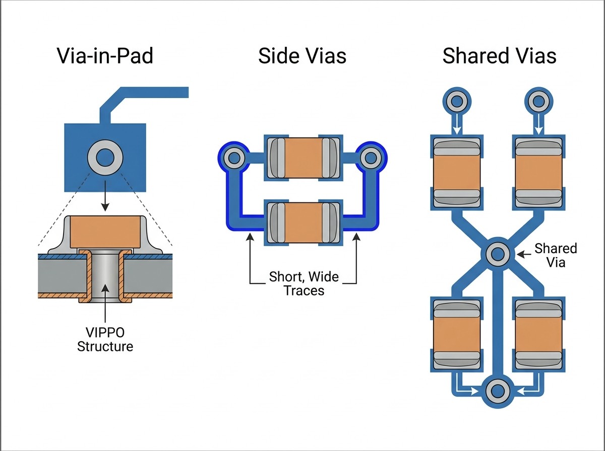
Via-in-Pad Plated Over (VIPPO / IPC-4761 Type VII): This configuration places the via directly within the capacitor pad, eliminating trace stubs entirely. Mounting inductance drops to approximately 0.3–0.5 nH, providing the cleanest high-frequency path. However, VIPPO requires via plugging, planarization, and capping—adding roughly 8 to 10 fabrication steps and increasing raw PCB manufacturing costs by an estimated 8% to 25%[4], according to ProtoExpress. For designs operating above 1 GHz, this premium is often justified.
Side Vias with Short, Wide Traces: Position vias immediately adjacent to the capacitor pads, connecting them with the widest and shortest traces practical. This approach typically achieves mounting inductance in the 1.0–2.0 nH range and represents a cost-effective compromise for sub-GHz digital designs.
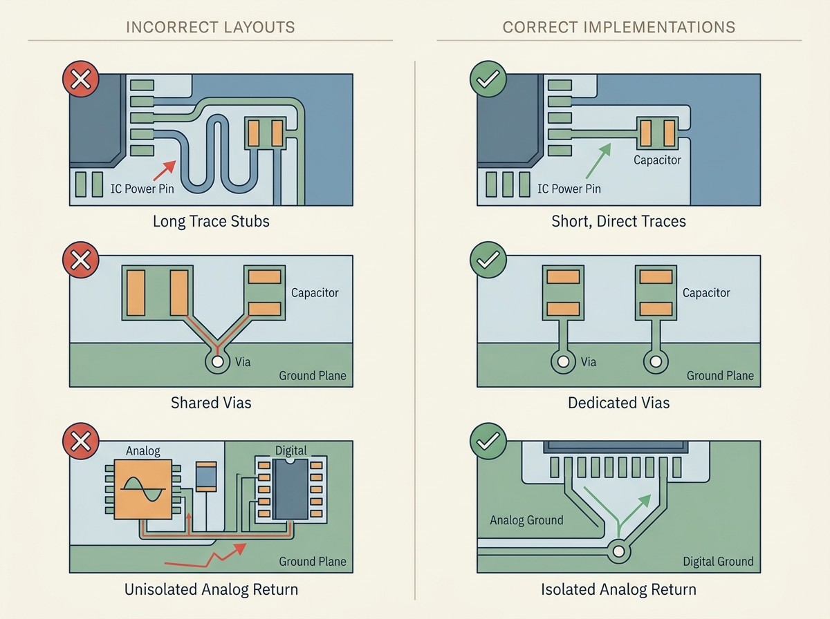
Shared Vias (Avoid): Routing multiple capacitor pads through a single shared via creates a daisy-chain current loop. Total loop impedance multiplies, and high-frequency crosstalk between capacitor networks increases. Dedicate separate vias to each capacitor pad for high-speed banks.
Reflow Path Considerations
The return current path is as important as the supply path. Ground return vias must offer an unobstructed, low-inductance route back to the IC reference ground. Any discontinuity in the reference plane beneath the decoupling loop elongates the return path and introduces additional inductance. For a deeper analysis, refer to our guide on PCB reflow and high-speed signal reflow path analysis.
Frequency Response and Placement Hierarchy: 10nF, 100nF, and 1uF MLCCs
Every real capacitor possesses a Self-Resonant Frequency (SRF) at which its capacitive and inductive reactances cancel[3]:
fSRF = 1 / (2 · π · √(LESL · C))
Below fSRF, the component behaves as a capacitor. Above fSRF, package inductance dominates and the device becomes inductive—completely useless as a decoupling element at those higher frequencies. This is why the common practice of populating a board with only 100nF capacitors is insufficient for modern high-speed designs.
Placement Hierarchy by Value
10nF (0201 package) — Closest to IC Pins/Vias:
Highest SRF, typically above 100–200 MHz when mounted. Handles the fastest switching transients at the GHz edge. Place these directly at the BGA pad/via interface or within a millimeter of exposed power pins.100nF (0402 package) — Mid-Band Decoupling:
Mounted SRF typically in the range of 15–30 MHz. Provides the bulk of the charge delivery for mid-range transients. Place adjacent to the 10nF components, routing directly into the same via cluster.1uF and Above (0603 to 1206 or Tantalum/Polymer) — Bulk Storage:
Low SRF (typically below 5 MHz). These handle low-frequency droop and board-level ripple. Place near the VRM output or at power entry boundaries rather than at each IC.
Mixing these values across the PDN creates a broadband, low-impedance profile and prevents the parallel anti-resonance impedance peaks that plague single-value decoupling schemes. For foundational capacitor concepts, see our introduction to filter capacitors.
Common Decoupling Layout Mistakes to Avoid
1. Long Trace Stubs Between Via and Capacitor Pad
A surface trace stub between the via and the landing pad typically adds approximately 1 nH/mm of parasitic inductance. A 2mm stub on each pad can double the mounted inductance of an 0402 capacitor, shifting the SRF downward and nullifying its high-frequency benefit.
2. Daisy-Chaining Power/Ground Vias
When multiple decoupling capacitors share a single via pair, the loop currents overlap. This multiplies the total loop impedance and reduces the effectiveness of every capacitor in the chain. Each capacitor pad should have its own dedicated via to the respective power and ground planes.
3. Placing Capacitors Without Considering Board Thickness
A decoupling capacitor placed on the opposite side of a 1.6mm board connects to the IC through through-hole vias that add approximately 0.5–1.2 nH per transition. Placing the same capacitor on the same side as the IC, with blind vias into the nearest plane pair, reduces that inductance.
4. Mixing Digital and Analog Decoupling Returns
Digital switching noise couples easily into sensitive analog domains when decoupling capacitor grounds share copper pours without isolation. Partition power planes and place ferrite beads between domains where necessary. Our guide on general PCB layout design guidelines for RF and digital-to-analog circuits covers mixed-signal partitioning in detail.
Power Integrity Layout Verification Checklist
[ ] Are 0201/0402 high-frequency capacitors connected to planes with minimal trace length?
[ ] Is the dielectric thickness between power and ground reference planes 10 mils or less?
[ ] Does every decoupling capacitor pad have its own dedicated via to the power/ground plane pair?
[ ] Are trace fanouts from capacitor pads kept as wide and short as possible?
[ ] Have parallel anti-resonance impedance peaks been verified via PDN simulation?
Sourcing High-Quality MLCCs for High-Speed Designs
Power integrity at multi-gigahertz speeds depends on precision passive components. MLCC characteristics—ESL, ESR, dielectric stability under DC bias, and temperature coefficient—must match the assumptions built into your EDA simulation models. Substandard or counterfeit capacitors shift SRF frequencies and increase PDN impedance, producing intermittent logic errors that are notoriously difficult to debug in production.
UTMEL Electronics supports hardware design teams and procurement departments with an extensive, ready-to-ship inventory of ultra-low ESR MLCCs, high-frequency bypass capacitors, and SMD ferrite beads from trusted global manufacturers. Every component is traceably sourced to ensure that the parasitic parameters on your datasheet match the physical device on your board. Whether you are optimizing an Altium PDN Analyzer model, running Cadence Sigrity simulations, or verifying multi-channel PDN impedance in Keysight ADS, component repeatability is non-negotiable.
Frequently Asked Questions
Q: What is the difference between a bypass capacitor and a decoupling capacitor?
A: While the terms are often used interchangeably, a decoupling capacitor functions as a local energy reservoir that prevents switching noise from propagating back onto the shared power rail. A bypass capacitor shunts unwanted high-frequency AC noise directly to ground at a specific node, preventing it from entering a sensitive circuit stage. Physically, they are the same component type—the distinction lies in where they sit in the circuit and what problem they solve.
Q: Why is dielectric thickness between power and ground planes so critical?
A: Thin dielectrics (10 mils or less) maximize the inherent interplane capacitance and, more importantly, dramatically reduce spreading inductance. This allows a decoupling capacitor placed anywhere on the board to couple effectively into the plane pair with minimal added parasitic inductance.
Q: Can I replace multiple 0.1µF capacitors with a single 1µF capacitor?
A: Generally not. A single 1µF component typically comes in a larger package size with higher ESL, resulting in a lower SRF. It cannot attenuate the high-frequency switching noise above 100 MHz that multiple smaller, low-ESL capacitors can handle. A mixed-value decoupling network with multiple package sizes provides broadband impedance control across the full PDN bandwidth.
Sources and references used for this guide
Decoupling Capacitor Optimization and Resources for Power Integrity
Source type: reputable professional source
Used for: Guidelines on PDN impedance and minimizing loop area.
Caution: EDA vendor application note; represents industry best practice, not a formal standard.Low Inductance Capacitors For High-Speed Decoupling
Source type: official company documentation
Used for: Physics of capacitor ESL, SRF, and package size impacts.
Caution: Component manufacturer documentation.AN105-A1 PCB Design and Layout Considerations
Source type: official company documentation
Used for: IC-side layout requirements and via placement strategies.
Caution: Specific to Renesas, but applicable as general IC vendor guidance.Decoupling Capacitor Placement Guidelines
Source type: vendor article
Used for: Via-in-pad recommendations and manufacturing considerations.
Caution: PCB manufacturer blog; good for practical layout constraints.Power Plane Segmentation and Decoupling Capacitor Placement
Source type: vendor article
Used for: Proximity to IC pins and plane stackup advice.
Caution: Manufacturer blog.
 UTMEL
UTMEL
We are the professional distributor of electronic components, providing a large variety of products to save you a lot of time, effort, and cost with our efficient self-customized service. careful order preparation fast delivery service
 Pull-Down Circuit Guide: Working Principle, Resistor Value, Circuit Design, and ApplicationsUTMEL26 June 2026500
Learn how pull-down circuits work, how to choose a pull-down resistor value, and how to design reliable microcontroller inputs, MOSFET gates, reset pins, and sensor interfaces.
Read More Smd Components Outlook 2026: Supply, Lead Times, and Sourcing OptionsUTMEL21 July 2026908
The 2026 electronic component market faces a selective shortage driven by AI infrastructure and electric vehicles. While active ICs face lead times up to 55 weeks, commodity SMD passives remain stable at 12–20 weeks. This procurement guide details key trends in MLCCs and circuit protection, outlining actionable strategy solutions like dual-sourcing and flexible footprints to mitigate supply chain risks.
Read More Decoupling Capacitor Placement Guide: Maximizing Power Integrity in High-Speed Digital PCBsUTMEL12 August 2026488
This technical guide details how to optimize decoupling capacitor layout to maximize Power Integrity (PI) in high-speed digital PCBs. It explains how switching ICs induce power rail noise, the physics of parasitic loop inductance, and the impact of stackup plane separation. Layout engineers will find practical strategies for via placement, anti-resonance mitigation across multi-value capacitor networks, and sourcing reliable low-ESR MLCCs.
Read More sar-adc-reference-driver-selection-managing-dynamic-kickback-noise-loop-stabilityUTMEL17 September 2026161
Precision SAR ADCs present high-speed dynamic switched-capacitor loads that demand instantaneous transient currents during bit trials. This guide details how to size local decoupling capacitors accounting for MLCC DC bias derating, stabilize reference buffers using dual-loop in-loop compensation, and minimize multiplicative noise degradation. It also provides layout directives and dynamic bench verification protocols across sampling rate sweeps and burst modes.
Read More HF PCB Circuit Design 10 QuestionsUTMEL16 March 20225523
Hello everyone, I am Rose. Today I want to give you a full explanation about PCB design. I Hope the following ten questions will give you a satisfied answer.
Read More
Subscribe to Utmel !
![MP4-1W-1W-10]() MP4-1W-1W-10
MP4-1W-1W-10Emerson
![NSS040A0X-62Z]() NSS040A0X-62Z
NSS040A0X-62ZGeneral Electric
![MP6-1W-1W-1W-4NE-4NN-00]() MP6-1W-1W-1W-4NE-4NN-00
MP6-1W-1W-1W-4NE-4NN-00Emerson
![BM2P063MF-ZE2]() BM2P063MF-ZE2
BM2P063MF-ZE2ROHM Semiconductor
![PQAE50-D24-S5-D]() PQAE50-D24-S5-D
PQAE50-D24-S5-DCUI Inc
![L6R160D-190-C6]() L6R160D-190-C6
L6R160D-190-C6Curtis Industries
![XG7]() XG7
XG7OptiFuse
![RPMH3.3-1.5]() RPMH3.3-1.5
RPMH3.3-1.5RECOM Power
![20A24-N15-I5-5PPM-F-M-1]() 20A24-N15-I5-5PPM-F-M-1
20A24-N15-I5-5PPM-F-M-1Advanced Energy
![20A24-P15-I10-5PPM-F-M-H-1]() 20A24-P15-I10-5PPM-F-M-H-1
20A24-P15-I10-5PPM-F-M-H-1Advanced Energy