Product
 Brand
Brand Articles
 Tools
Tools
eFuse Capacitive Load Startup: Calculate Inrush Current and Prevent Hiccup Trips
Quick answer: calculate capacitor charging current from I = C × dV/dt, add the load current present during startup, and check the resulting voltage–current–time trajectory against the selected eFuse's startup limits. Keep demanding downstream converters disabled until the protected rail is ready. Then verify input voltage, output voltage, current, and status signals together. A flat output ramp can indicate a load-current problem; a shutdown does not, by itself, prove thermal overload.
1. Define the startup conditions before selecting components
Start with the circuit as it will be powered in service. A bench supply connected through short leads may behave differently from a shared industrial bus reached through a long cable. Likewise, an unpowered converter input is different from a converter that begins switching halfway through the charging ramp.
| Design input | What to record | Why it changes the result |
|---|---|---|
| Supply | Minimum and maximum voltage, current budget, current-limit behavior, wiring impedance | Determines charging energy and whether the source collapses during startup |
| Output capacitance | Effective capacitance over voltage and temperature, tolerance, ESR, initial voltage | Sets charge demand; a discharged bank is different from a partially charged one |
| Startup load | Leakage, bleeder current, converter enable threshold, soft-start demand | Current diverted into the load is unavailable for capacitor charging |
| Timing | Required rail-ready time, enable delays, retry policy | Establishes whether a slower ramp is acceptable |
| Protection device | Exact orderable suffix, startup mode, current-limit tolerance, timer conditions | Similar-looking eFuses can react differently to the same ramp |
| Thermal environment | Starting temperature, PCB copper, exposed-pad assembly, repetition rate | Determines available thermal margin |
For a bank whose capacitance changes materially with voltage, use its effective capacitance curve instead of one nominal value. Charging stress and hold-up capacity may require different corners: the larger effective capacitance increases startup demand, while the smaller value reduces stored charge available to the load.
2. Calculate eFuse startup inrush current and ramp time
Let VO be the protected output voltage and IL the load current drawn from that rail. Neglecting the eFuse's small internal supply current, the current balance is:
IFET(t) = CO × dVO/dt + IL(t)
For a linear ramp from an initial voltage V0 to a target VT in time tr, with approximately constant capacitance and load current:
IC = CO × (VT − V0)/tr
tr = CO × (VT − V0)/(IFET − IL)
The denominator must remain positive. If the load consumes all available current, the capacitor stops charging. If the load consumes more, the capacitor supplies the difference and its voltage falls. This simple balance is often more useful than changing the slew-rate capacitor by trial and error.
For a programmed ramp, check that the maximum required charging-plus-load current stays below both the source's available current and the eFuse's minimum current-limit threshold. If the current limit becomes active, the output no longer follows the nominal slew-rate setting. Thermal foldback, startup power control, and source droop can reduce the available current further.
A slew-rate capacitor is also device-specific. Use the equation for the exact eFuse and startup mode; do not transfer a capacitor value between different families. TI's TPS2663x datasheet, for example, gives the nominal relationship below, with time in seconds, input voltage in volts, and capacitance in farads. TPS2663x datasheet, §8.3.1
tdVdT = 20.8 × 10³ × VIN × CdVdT
This predicts the programmed ramp. It does not include every delay between applying power and reaching a usable system state.
3. Worked example: a 24 V rail with a 4.7 mF bank
The following inputs are illustrative design assumptions, not measured board data or guaranteed ratings for a selected part. Assume an initially discharged bank, a constant supply during each attempt, and downstream converters held off. Allow 2.4 A for capacitor charging after reserving any other startup demand.
| Quantity | Nominal assumption | Stress assumption |
|---|---|---|
| Input voltage | 24 V | 28.8 V |
| Output capacitance | 4.7 mF | 5.64 mF, representing +20% |
| Requested linear ramp | 50 ms | Initially keep 50 ms to expose the current requirement |
| Available capacitor current | 2.4 A | 2.4 A |
At nominal conditions, a 50 ms ramp requires:
IC = 0.0047 × 24/0.050 = 2.256 A
At the higher voltage and capacitance, forcing the same ramp duration requires:
IC,max = 0.00564 × 28.8/0.050 = 3.249 A
That exceeds the assumed budget. The shortest constant-current charging time at that corner is:
tr,min = 0.00564 × 28.8/2.4 = 67.68 ms
If using the TPS2663x relationship above, a candidate 150 nF slew capacitor gives nominal ramp times of 74.88 ms at 24 V and 89.856 ms at 28.8 V. The latter charges 5.64 mF at approximately 1.808 A. These are calculations from the published relationship, not guaranteed startup times.
For an assumed −10% slew-capacitor corner, CdVdT becomes 135 nF and the same maximum bank requires approximately 2.009 A using the nominal device coefficient. That fits the assumed 2.4 A allocation before accounting for the device's own slew-rate tolerance. Complete that tolerance check, along with eFuse current-limit and source tolerances, before selecting the final component value. Also check the opposite corner for the longest acceptable startup.
What this example establishes: a nominal 50 ms calculation can hide a current-budget failure at the worst corner. It does not establish thermal feasibility. The next calculation is needed even when the current arithmetic passes.
4. Calculate pass-FET energy without confusing it with temperature
During charging, the series transistor operates with substantial voltage across it. Its instantaneous dissipation is approximately:
PFET(t) = [VIN − VO(t)] × IFET(t)
For constant VIN, constant capacitance, no active load, and negligible losses elsewhere, integration over a charge from V0 to VT gives:
EFET = CO{VIN(VT − V0) − (VT2 − V02)/2}
When VT equals VIN, this becomes ½CO(VIN − V0)². For a fully discharged bank, it reduces to the familiar result:
EFET = ½COVIN2
The worked example therefore dissipates approximately 1.354 J nominally and 2.339 J at the higher voltage and capacitance. The calculation assumes the pass transistor takes essentially the entire series voltage drop. Significant resistor or capacitor-ESR loss redistributes that energy; a changing input rail requires integrating the actual waveforms.
With an active load, an additional term appears: the integral of [VIN − VO(t)] × IL(t) over startup. Thus ½CV² alone can underestimate transistor energy in a powered system.
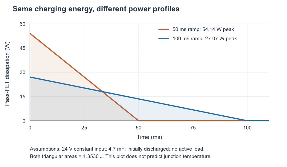
Why a slower ramp can help
For a capacitor-only linear ramp, doubling the duration halves the current and peak dissipation while preserving total energy. During the longer event, heat can also leave the junction. Equal energy does not imply equal peak junction temperature. The increase of transient thermal impedance with time is insufficient, by itself, to conclude that a slower startup runs hotter: the applied power has changed at the same time.
There is no universal joule rating for all eFuses in a particular package size. Use device-specific startup curves or a validated thermal model with the relevant PCB conditions. A joule calculation is a stress indicator, not a substitute for a safe operating area check.
For a rectangular power pulse, temperature rise can be estimated from pulse power times transient thermal impedance, using the correct junction-to-case or junction-to-ambient reference. A normalized impedance curve must first be multiplied by its reference thermal resistance. Repeated pulses require the appropriate duty-cycle treatment. TI SLUAAT8, §§2–3
An actual charging ramp has varying power. Split that waveform into suitable time segments and apply the thermal response consistently, or use the manufacturer's design tool. Avoid multiplying average power by an arbitrarily chosen impedance and treating the result as an exact peak temperature. External pass MOSFETs also require a linear-mode SOA check at the relevant temperature and pulse duration. TI SLVA158, thermal-response and SOA discussion
5. Separate slew control, current limiting, thermal regulation, and fault timers
Several control functions can shape one startup attempt. Identify the active function before deciding whether to speed up or slow down the ramp.
| Function | What it controls | What to check during startup |
|---|---|---|
| Slew-rate control | Requested output-voltage rise | Whether another control loop prevents the requested ramp |
| Current limiting | Maximum delivered current | Remaining capacitor current after the load turns on |
| Pass-FET power limiting | Dissipation across the series transistor | Applicable operating region and any associated timeout |
| Startup thermal regulation | Current profile in response to junction heating | Entry conditions, completion rules, and timeout |
| Output power limiting | Power delivered to the load | Availability on the selected suffix and operating state |
| Shutdown or circuit breaker | Termination of an overload or unsafe state | Trigger condition, timer start point, and recovery mode |
These quantities are distinct by definition: output power is VOIO, while series-transistor dissipation is approximately (VIN − VO)IO. A device advertised with output power limiting does not, from that label alone, promise a particular transistor-dissipation limit.
A timer need not run throughout the entire voltage ramp. It may begin only after a current threshold is exceeded, after thermal regulation starts, or in a particular fault state. Compare the time spent in the timed state with that timer's minimum allowed duration. Do not impose a generic “all startup must finish within a few milliseconds” rule.
TPS2663x illustrates this distinction: it provides startup thermal regulation and a separate regulation timeout. Its electrical-characteristics table lists tTreg_timeout as 2.3 s minimum, 2.54 s typical, and 2.9 s maximum. This is not permission to exceed other startup constraints or operate indefinitely in regulation. TPS2663x datasheet, timing table and §8.3.1.1
TI's large-capacitor application note demonstrates thermal-regulated startup, including 4.7 mF and 20 mF examples at 32 V. Treat those results as demonstrations under the reported conditions, not a universal guarantee for every capacitor bank or ambient temperature. TI SLVAEB9A, §4
6. Keep downstream converter startup from consuming the charging current
A regulated converter can demand more input current at low input voltage. As a simplified operating approximation, a converter delivering power PLOAD with efficiency η draws:
IL ≈ PLOAD/(η × VO)
This model describes a converter already regulating approximately constant output power. It does not describe behavior all the way down to zero input voltage; UVLO, soft-start, current limiting, and control dynamics determine the real startup waveform.
For an illustrative 12 W load and assumed 90% efficiency, the input demand at 5 V is about 2.667 A. If the eFuse can supply only 2.4 A at that moment, the calculated net capacitor current is −0.267 A. For the example's 4.7 mF bank, the instantaneous voltage slope is approximately −56.7 V/s. The circuit may sag below converter UVLO and restart instead of progressing toward the full rail.
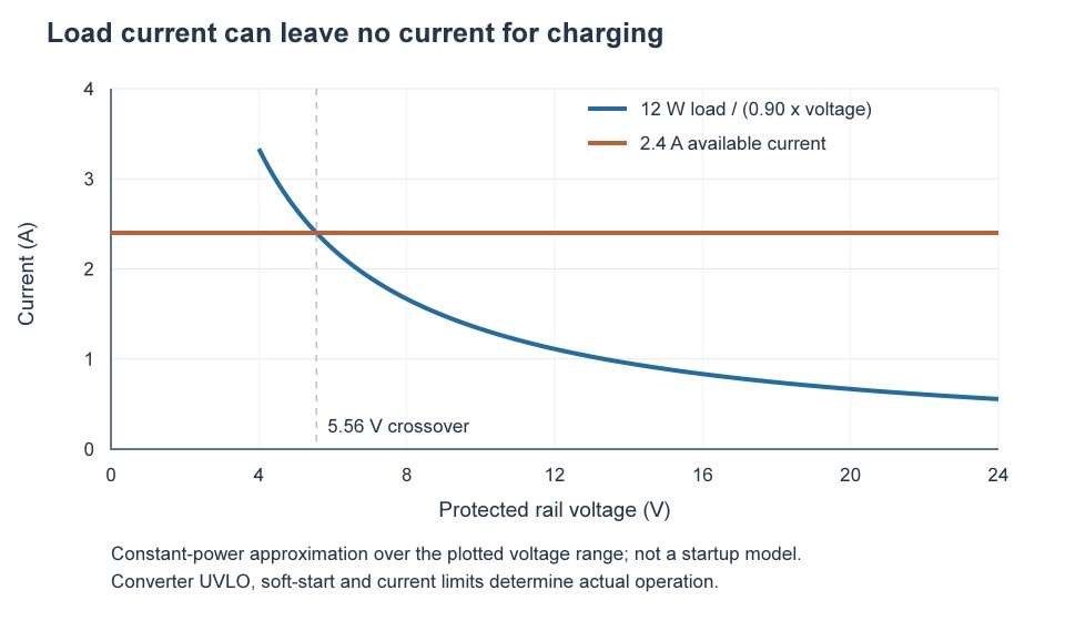
Sequencing removes much of this uncertainty. Keep the converter disabled while charging the bulk rail, then release its enable when the eFuse and rail satisfy the required ready conditions. TPS2663x provides an open-drain PGOOD signal qualified by its PGTH input and internal-FET enhancement state. TPS2663x datasheet, §8.3.2
For the actual interconnection, verify the PGOOD pull-up voltage, converter EN absolute maximum, logic thresholds, sink-current requirement, and behavior when either supply is absent. A level translator or supervisor may be necessary. Do not connect a high-voltage rail directly to a low-voltage EN input simply because both signals are called “enable” or “power good.”
After the capacitor has charged, the converter still needs to start. Check that its soft-start current and the combined steady load fit the protection settings, and that enabling the load does not pull the rail back below the ready threshold. Include bleeders, leakage, and any circuitry that remains powered while EN is low in the initial current budget.
7. Choose the architecture from the stress and timing requirements
Capacitance alone cannot select an eFuse topology. A large bank charged slowly at low voltage may be easier to handle than a smaller bank charged quickly at high voltage.
| Architecture | Useful when | Decision still required |
|---|---|---|
| Integrated eFuse with adjustable slew | A defined load can start within documented current, thermal, and timing limits | Verify worst-case ramp and powered-load behavior |
| Integrated eFuse with startup thermal regulation | Load capacitance or thermal conditions vary enough to make a fixed ramp difficult | Verify allowed operating states, timeout, and rail-ready deadline |
| Hot-swap controller with external MOSFET | The design needs a separately chosen pass device and thermal layout | Check linear-mode SOA, controller protection, gate drive, and PCB heat removal |
| Managed precharge path followed by bypass | Charging time and dissipation can be assigned to a dedicated path | Rate precharge components for pulse stress and ensure faults remain protected |
This is a design comparison, not a substitution table. Changing architecture requires reviewing the protection circuit and layout; package size or nominal on-resistance does not establish compatibility. Integrated and discrete approaches both need checks against the actual load and fault conditions. TI Basics of eFuses, §§2–3
For resistor precharge into an ideal, unloaded capacitor, the initial current is (VIN − V0)/R and the time to reach a chosen threshold follows the RC charging curve. A target close to the supply takes longer than one time constant. Specify the bypass threshold, residual voltage step, resistor pulse-energy rating, and failed-bypass behavior. Do not add a parallel path that silently defeats the required short-circuit protection.
8. Check the input supply, TVS, and physical layout
Two different events deserve separate captures: the current demand as the rail rises, and the voltage transient when current is interrupted. For wiring inductance L, the voltage associated with a current change has magnitude approximately L × |di/dt|; its polarity depends on the observation point and current direction.
An input TVS limits a transient at its connection point. It does not set the output-voltage ramp or replace the capacitor-current calculation. If input voltage collapses during charging, investigate the source's current-limit mode, lead resistance, connector drop, and local bypass network before changing the TVS.
Choose transient protection from the maximum continuous input, the applicable surge waveform and source impedance, clamp voltage at the relevant pulse current, temperature, repetition, and the eFuse's absolute-maximum limits. Include layout-induced overshoot. A TVS part number chosen solely because the bus is nominally 24 V is insufficient. Keep the transient-current path short and follow the selected eFuse's layout guidance. TPS2663x datasheet, §§9.2 and 9.5
For a hold-up bank, also consider power removal: the charged output can exceed the input. Reverse-current protection is a separate function whose implementation varies by device. TI Basics of eFuses, §3.4
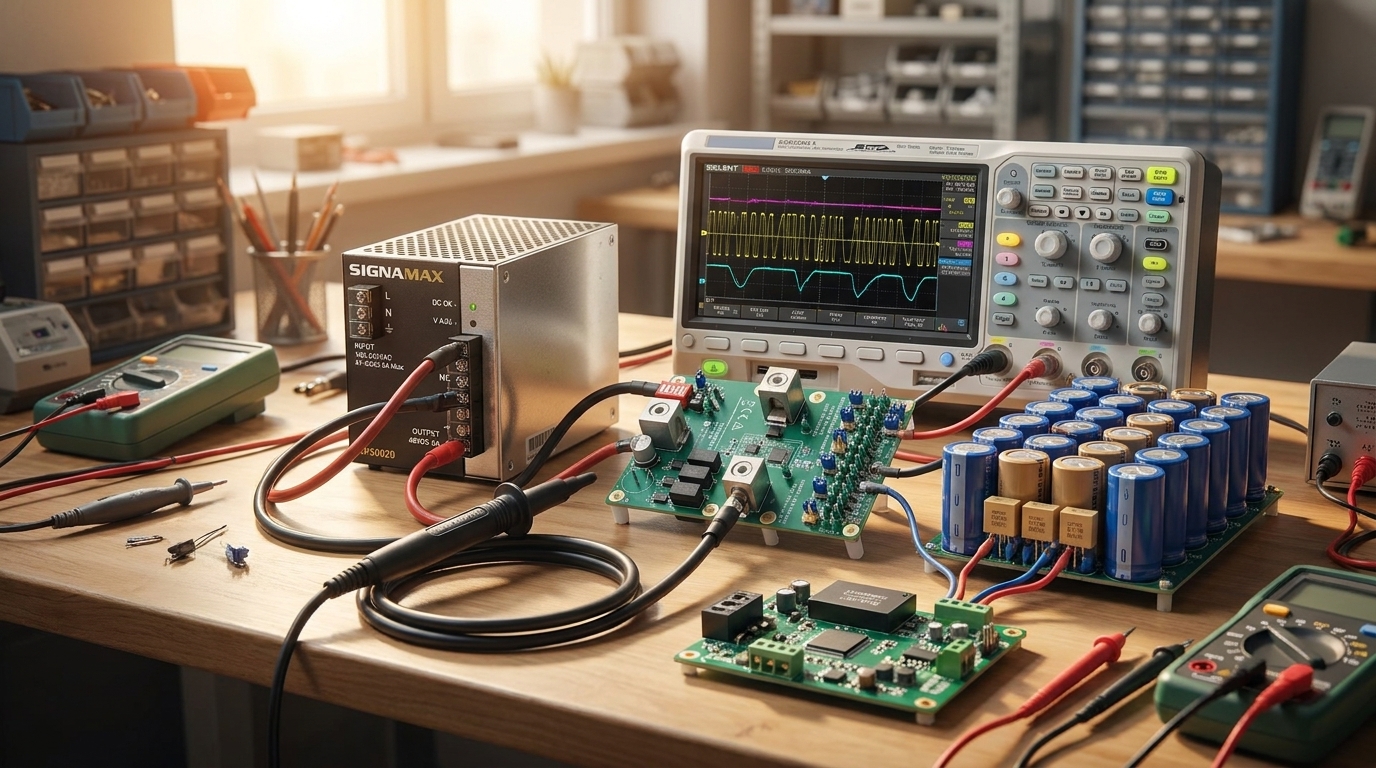
9. Use four oscilloscope channels to find what ends the ramp
Trigger on eFuse enable or the start of input power, and capture the complete attempt plus the next retry. Use a second, faster acquisition to inspect cutoff ringing; one time scale rarely shows both startup timing and a fast transient clearly.
| Channel | Probe location | Question it answers |
|---|---|---|
| CH1: input voltage | At the eFuse input and its local return | Does the source droop, cross UVLO, or overshoot at cutoff? |
| CH2: output voltage | Across the protected capacitor bank | Does voltage rise smoothly, plateau, discharge, or advance over retries? |
| CH3: pass-path current | In a suitable low-inductance measurement location | Is current following the predicted ramp, limiting, or changing with the load? |
| CH4: status | FLT or PGOOD, with an electrically valid pull-up | Which transition aligns with the voltage/current event? |
Measure the pass path if possible. A current probe upstream of a local input capacitor can show source current that differs from instantaneous FET current. If using a shunt, account for its voltage drop and measurement common mode. Use appropriately rated differential probing where required; avoid grounding a non-ground node with an earth-referenced probe clip.
FLT and PGOOD are not interchangeable diagnostic signals. If only one status channel is available, repeat the capture with the other signal, or use logic channels. Probe bandwidth should resolve the event being investigated; a millisecond ramp and a fast cutoff require different acquisition choices.
Waveform-based troubleshooting
| Observed pattern | Candidate explanation | Discriminating check and next action |
|---|---|---|
| Output flattens when a converter enables; current rises | Active load consumes the available charging current | Hold the converter disabled and repeat; review sequencing and startup demand |
| Current is limited, then the eFuse shuts down after a repeatable interval | A timer associated with that operating state expires | Measure from the relevant trigger condition and compare with the specific timer limits |
| Current folds back and the ramp continues slowly | Startup thermal or power control is active | Compare with the documented behavior; verify completion before timeout |
| Mid-ramp cutoff becomes more frequent on a hot board | Thermal margin may be insufficient | Compare hot/cold captures and the actual power profile; review PCB and startup limits |
| Input collapses before output stops rising | Source current limiting, wiring drop, or UVLO cycling | Measure at both source and eFuse; change one supply-path variable at a time |
| Input spikes when current turns off | Inductive interruption transient | Inspect probe technique, clamp path, local bypass, and layout |
| Output rises a little on each retry, or repeatedly returns to the same level | Charge retained between attempts, or lost again into the load | Compare charge gained while on with discharge while off; inspect retry and discharge behavior |
These signatures narrow the investigation; they do not uniquely identify a fault without the device's status rules and timing information. In particular, a long recovery interval alone is not a temperature measurement.
10. Validate the complete startup sequence
Use a repeatable set of corner tests rather than treating one successful cold start as the result.
Discharged-bank startup: confirm initial output voltage, source conditions, current peak, charging time, and status sequence.
Load-enabled startup: repeat with the real converter sequence and measure the current step when each load starts.
Voltage and capacitance corners: test the intended extremes, including the source's own current-limit behavior.
Temperature and repetition: test a cold board, a warm board, and the intended restart cadence; record whether each attempt begins from a comparable state.
Brownout and partial discharge: verify recovery from residual output voltage and check reverse-current behavior when input power disappears.
Fault and recovery: confirm the configured response and reset sequence under controlled fault conditions.
Input interruption transients: measure local input and output excursions and compare them with the relevant device limits.
Record the exact device suffix, board revision, input wiring, capacitor population, ambient conditions, and oscilloscope settings with each capture. Define acceptance as a rail reaching its required voltage within the allowed system time, enabling the intended load, and remaining stable without unexpected retries or limit violations.
11. Frequently asked questions
Will a larger slew-rate capacitor always fix startup?
No. It can reduce charging current, but a load consuming that current, an applicable timeout, or an unstable input source can still prevent completion. Verify which control function is active and recalculate both current and time.
Is ½CV² the eFuse's allowable startup energy?
No. It estimates dissipated energy for a specific ideal charging case. Allowable stress depends on the device, power waveform, temperature, thermal path, and repetition. It cannot be treated as a package rating.
Can repeated hiccup attempts eventually charge the bank?
They can if each attempt adds more charge than the bank loses while the switch is off. An active load or output-discharge circuit may prevent this. Auto-retry is an intentional feature on some devices; whether it is acceptable for normal startup depends on the documented behavior and the system's timing and stress requirements. Do not infer inevitable device damage solely from the presence of retries.
Does thermal regulation allow unlimited capacitance?
No. A thermal-control loop changes the current profile, but charging still takes time. Its timeout, source capability, active load, and system deadline remain constraints. Validate the largest specified load rather than interpreting “unknown capacitive loads” as an unlimited rating.
Should the downstream EN pin be connected directly to PGOOD?
Only when their voltage ratings, logic thresholds, polarity, and power-off behavior are compatible. Set the rail-ready condition intentionally and verify the load's subsequent startup. Use suitable interface circuitry where a direct connection is unsuitable.
When is precharge preferable?
Consider it when a controlled charging path better meets the required energy, timing, and component-stress budget. There is no universal capacitance threshold. Account for bypass inrush and fault protection as well as the initial RC charge.
12. Conclusion
A dependable eFuse startup design begins with the charge balance and ends with the complete system sequence. Budget capacitor and load current together, evaluate the pass transistor over the actual ramp, apply each timer to its documented operating state, and verify the source and downstream enable behavior on the bench. Those checks turn a repeated restart into a diagnosable event and a component choice into a design that can be validated.
References
Texas Instruments, Reliable Start-up with Large and Unknown Capacitive Loads, SLVAEB9A, revised February 2022. Startup architectures and demonstrated capacitive loads.
Texas Instruments, TPS2663x datasheet, SLVSE94G, revised June 2024. Startup equations, regulation timeout, status logic, application design, and layout.
Texas Instruments, Basics of eFuses, SLVA862A, revised April 2018. Protection functions and fault-recovery distinctions.
Texas Instruments, Using MOSFET Transient Thermal Impedance Curves In Your Design, SLUAAT8, December 2023. Normalized thermal impedance and repetitive pulses.
Texas Instruments, Hotswap Design using TPS2490/91 and MOSFET Transient Thermal Response, SLVA158, July 2004. Thermal-response modeling and SOA evaluation.
 UTMEL
UTMEL
We are the professional distributor of electronic components, providing a large variety of products to save you a lot of time, effort, and cost with our efficient self-customized service. careful order preparation fast delivery service
 eFuse Capacitive Load Startup: Calculate Inrush Current and Prevent Hiccup TripsUTMEL14 September 202613
An eFuse that repeatedly restarts while charging a capacitor bank needs three checks: how much current reaches the capacitor, how long the pass transistor can sustain the resulting dissipation, and which protection function actually ends the attempt. Reducing the programmed slew rate often helps, but the result also depends on the active load, supply behavior, and the device's startup state machine.
Read More Fuse Design and Selection PointsUTMEL01 July 20227821
Hello, this is Candy. Today I would like to have a discussion about Fuse Design and Selection Points.
Read More The Introduction of Car FuseUTMEL09 October 20217000
A small tubular fuse, which consists of two major parts: a tube body with metal connection terminals on both ends and a metal melt in the tube, is the most widely used in circuit overcurrent safety components. This article introduce its relevant knowledge in car.
Read More How does a Resettable Fuse Work?UTMEL26 August 202037713
A resettable fuse is a kind of over-current electronic protection component. It is made of a high-molecular organic polymer under high pressure, high temperature, and sulfidation reaction. It's mixed with conductive particle materials, and processed by special technology.
Read More How Electric Fuses Work: Types, Ratings, and Selection GuideUTMEL14 July 202618210
This guide walks through how a fuse actually interrupts a fault, the difference between fast and slow elements, the main fuse families and where each one belongs, the ratings that genuinely matter, and a repeatable method for choosing a fuse for your own circuit. It closes with the mistakes that most often cause either nuisance opening or unsafe under-protection, a clear comparison with circuit breakers, and a frequently asked questions section.
Read More
Subscribe to Utmel !
![MTKCA-0500-0300]() MTKCA-0500-0300
MTKCA-0500-0300Omron
![XZM:50458160006000]() XZM:50458160006000
XZM:50458160006000Siemens
![6SL33307TG374AA3]() 6SL33307TG374AA3
6SL33307TG374AA3Siemens
![3UG48222AA40]() 3UG48222AA40
3UG48222AA40Siemens
![6AV63711DN072CX0]() 6AV63711DN072CX0
6AV63711DN072CX0Siemens
![3RT1036-3BD40]() 3RT1036-3BD40
3RT1036-3BD40Siemens
![AFM40-N04-8Z-A]() AFM40-N04-8Z-A
AFM40-N04-8Z-ASintered Metal Company
![KQ2F01-34-X23]() KQ2F01-34-X23
KQ2F01-34-X23Sintered Metal Company
![MGGLB32-400-XC37]() MGGLB32-400-XC37
MGGLB32-400-XC37Sintered Metal Company
![49EC18EW362412R]() 49EC18EW362412R
49EC18EW362412RSiemens