What is Chiplet?

How AMD is Making CPUs More Affordable - Chiplets Explained
Catalog |
Ⅲ The three major values of chiplets: fast development, low cost, and multiple functions |
Ⅰ What is Chiplet
10nm, 7nm, 5nm... As chip process nodes become more and more advanced, R&D and production costs continue to rise, and yields are declining, and physical bottlenecks are dragging down the pace of Moore's Law.
Chiplets like Lego bricks are becoming one of the common choices of AMD, Intel, TSMC, Marvell, Cadence, and other chip giants to continue Moore's Law.
In the past, chips were integrated and packaged into a single chip by multiple IP cores. However, the chiplet method can combine chiplets designed and packaged from different companies to build a more efficient and economical chip system.

monolithic chip and chiplets
This new design method not only greatly simplifies the complexity of chip design, but also effectively reduces design and production costs.
Omdia, a well-known market research organization, predicts that the global market for chiplets will expand to US$5.8 billion in 2024, a 9-fold increase from the US$645 million in 2018. In the long run, the chiplet market is expected to increase to 57 billion U.S. dollars in 2035.
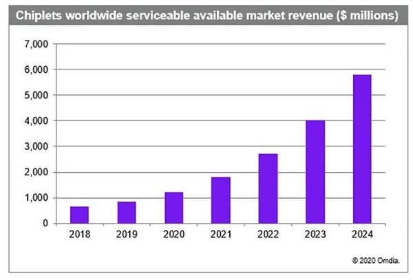
Global Chiplet Market Revenue 2018-2024 (Source: Omdia)
Ⅱ Continue Moore's Law! The era of chiplets is here
Fifty-five years ago, Moore's Law, which was praised as the "Bible" of the chip industry, predicted that when the price remains the same, the number of transistors that can be accommodated on an integrated circuit will double every 18 to 24 months, and the performance will also double.
The emergence of Moore's Law set a critical benchmark for the pace of technological development, catalyzed the prosperity of the technology market, and brought immeasurable economic value to the entire IT industry.
There are many benefits of using advanced nodes including greater transistor density, less space, higher performance, and lower power, but the challenges are becoming more and more difficult to overcome.
With extremely small sizes, chip physical bottlenecks are becoming more and more difficult to overcome. Especially in recent years, when advanced nodes are moving towards 10nm, 7nm, and 5nm, the problem is no longer just a physical obstacle. The more nodes evolve, the higher the cost of miniaturization, and there are fewer and fewer design companies that can bear the economic burden.

Rapid growth in chip costs as process nodes evolve
According to public reports, the design cost of the 28nm node is about US$50 million, and to the 5nm node, the total design cost has soared to more than US$500 million, which is equivalent to more than 3.5 billion yuan.
Keeping Moore's Law is about maximizing profits. If R&D and production costs cannot be reduced, then it will be a terrible financial burden for chip giants and startups.
Fortunately, whenever Moore's Law is walked to an end, scientists and engineers will always inspire innovative ideas, put forward breakthrough technologies to turn the tide, and repeatedly push the seemingly end of Moore's Law to the distance.
The modular design based on chiplets is one of the most critical ideas to solve the cost problem.
Ⅲ The three major values of chiplets: fast development, low cost, and multiple functions
The current chip design model often buys soft-core IP or hard-core IP from different IP vendors, and then integrates self-developed modules into a system-on-chip (SoC), and then produces chips at a certain manufacturing process node.
With advanced packaging technology, chiplets can integrate a variety of different architectures, different process nodes, and even dedicated silicon blocks or IP blocks from different foundries. You can skip tape out and quickly customize one that can meet multiple functions.
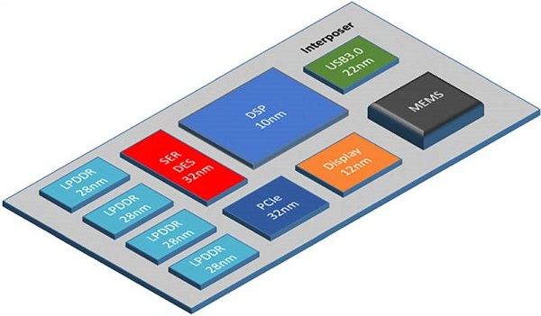
Small chip system consisting of multiple small chips on an intermediary layer (source: Cadence)
The benefits of a monolithic chip over a single chip are obvious.
First, the development of chiplets is faster.
In computing systems such as servers, power and performance are dominated by CPU cores and caches. By combining the memory and I/O interfaces on a single I/O chip, the bottleneck delay between the memory and I/O can be reduced, thereby helping to improve performance.
Second, the development cost of chiplets is lower.
Because the chiplet is composed of different chip modules, designers can choose the most advanced technology in a specific design part, and choose more mature and inexpensive technology in other parts, thereby saving the overall cost.
For example, AMD’s second-generation EPYC server processor Ryzen uses a chiplet design, combining a more advanced CPU module manufactured by TSMC’s 7nm process and a more mature GlobalFoundries 12/14nm process I/O module. 7nm can meet the demand for high computing power while 12/14nm can reduce manufacturing costs.
The benefit of this is that the chip area of the 7nm process part is greatly reduced, and the use of more mature process I/O modules will help improve the overall yield and further reduce the cost of foundry. On the whole, the more CPU cores, the more obvious the cost advantage of the chiplet combination.
Finally, chiplets can flexibly meet different functional requirements.
On the one hand, the chiplet solution has good scalability. For example, after constructing a basic die, only one die may be used for laptops, two for desktop computers, and four for servers.
On the other hand, chiplets can act as heterogeneous processors, combining different processing elements such as GPUs, security engines, AI accelerators, and IoT controllers in any number to provide richer acceleration options for various application needs.
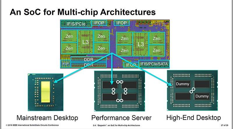
an soc for multi-chip archirectures
As the advantages of chiplets are gradually revealed, it is being adopted by more advanced and highly integrated semiconductor devices such as microprocessors, SoCs, GPUs, and programmable logic devices (PLD).
According to statistics from research institute Omida, microprocessors are the largest market segment for chiplets, and the market share of microprocessors supporting chiplets is expected to grow from US$452 million in 2018 to US$2.4 billion in 2024.
At the same time, the computing field will become the main application market for chiplets, which is expected to account for 96% of the total revenue of chiplets this year.
Ⅳ Chiplet is being standardized
Chip giants are particularly alert to changes, and no one wants to fall from the altar. While guarding the most advanced design and manufacturing technology, they must explore new feasible paths for themselves in advance.
Because of this, chip leaders such as Intel and AMD have not only become the earliest adopters and advocates of chiplets, but also core contributors to promote the standardization of chiplets.
As early as 2014, Huawei HiSilicon and TSMC had collaborated to show off a network chip using TSMC’s CoWoS technology, combining 16nm 32-core Arm Cortex-A57 with 28nm logic and I/O chips, and the speed is 40% faster than 28nm HPM at the same power consumption.
In 2016, Marvell and Kandou Bus announced an agreement. Marvell uses Kandou Glasswing IP as the chip-to-chip interface to connect multiple chips.
The US Department of Defense Advanced Research Projects Agency (DAPRA) launched the "Common Heterogeneous Integration and IP Multiplexing Strategy (CHIPS)" project in August 2017. This is the "Electronic Renaissance Program (ERI)" with a total investment of US$1.5 billion by DAPRA. Part of it is intended to promote a compatible, modular, and reusable chiplet ecosystem.
These chiplets can quickly mix and match various types of third-party chips into a system like piles of wood, realizing rich functions such as data storage, signal processing, and data processing. It can also reduce the overall size of the circuit board to the size of a conventional chip, therefore improving energy efficiency.
Ideally, with the help of the chiplet approach, chip design companies only need to focus on the IP they are good at, without worrying about other IPs, which not only helps to improve core innovation capabilities, but also amortizes R&D costs through multiple IP designs.
DAPRA extended an olive branch to chip companies such as Intel, Mecco, Cadence, and Sinos Technology, as well as some large military industry companies and university scientific research teams, and invited them to be the main contractors of the project.
As one of the core members of the CHIPS project, Intel introduced the Advanced Interface Bus (AIB) as a royalty-free die-to-die interface standard for chiplet architecture.
For example, Intel's Stratix 10 and Agilex FPGAs all use the same AIB interface to integrate a variety of different chiplets. With the support of the CHIPS project, many different companies and universities are using AIB to build chiplet systems.
Intel is also a member of the Open Computing Project Open Domain Specific Architecture (OCP ODSA) Foundation, which is promoting the development of standards and technologies to help implement advanced packaging strategies.
Intel uses its server processors, FPGAs, PC chips, etc. as commercial testing grounds for chiplet technology, and AMD also uses chiplets in server and client CPUs.
In 2017, AMD used chiplets to develop the Epyc server processor Naples in its Zen 2 architecture, and then supported 8 chiplets in the enterprise-level EPYC processor Rome, which was launched the following year, with a maximum of 64 cores.
AMD's Zen 2 processor series launched in 2019 has single-core performance surpassing Intel for the first time.
Ⅴ Conclusion: A low-cost path to the next node
Chiplets are not perfect now. On the way of exploring chiplets, traffic congestion, heat dissipation, power management, testing, and other issues are the main challenges to be overcome in system architecture design.
Although there are projects such as DAPRA CHIPS, OCP ODSA, etc. that are working hard to promote the standardization of chiplet interfaces, it is not yet known when the business model of independent third-party chiplet supply will become popular in the chip industry.
It may be difficult to save Moore’s Law by any method, but it is undeniable that the emerging method of chiplets is changing the design and integration strategy of chips, and it provides chip companies with more flexible mix and match system solutions. It is a low-cost path to migrate to the next node.
It is undoubtedly an exciting thing to be at the beginning of such a new revolution.
1.Does Intel use Chiplet?
Intel Embraces Chiplets

Using the technology, “we are now able to increase core counts, caches, memory, and I/O,” Biswas said. If this sounds familiar, that's because AMD did the same thing four years ago with its EPYC, ThreadRipper, and later Ryzen processor families.
2.Who manufactures Chiplets?
Intel to manufacture Qualcomm chips, package AWS chiplets. Months after launching its own foundry business, Intel has announced its first major customers: Qualcomm and Amazon Web Services. The company, which has fallen behind in market share and technical achievements, said that it hopes to regain its lead by 2025.
3.What is Chiplets in semiconductor?
A chiplet is an integrated circuit block that has been specifically designed to work with other similar chiplets to form larger more complex chips. In such chips, a system is subdivided into functional circuit blocks, called "chiplets", that are often made of reusable IP blocks.
 Discovering New and Advanced Methodology for Determining the Dynamic Characterization of Wide Bandgap DevicesSaumitra Jagdale15 March 20242450
For a long era, silicon has stood out as the primary material for fabricating electronic devices due to its affordability, moderate efficiency, and performance capabilities. Despite its widespread use, silicon faces several limitations that render it unsuitable for applications involving high power and elevated temperatures. As technological advancements continue and the industry demands enhanced efficiency from devices, these limitations become increasingly vivid. In the quest for electronic devices that are more potent, efficient, and compact, wide bandgap materials are emerging as a dominant player. Their superiority over silicon in crucial aspects such as efficiency, higher junction temperatures, power density, thinner drift regions, and faster switching speeds positions them as the preferred materials for the future of power electronics.
Read More A Comprehensive Guide to FPGA Development BoardsUTMEL11 September 202513865
This comprehensive guide will take you on a journey through the fascinating world of FPGA development boards. We’ll explore what they are, how they differ from microcontrollers, and most importantly, how to choose the perfect board for your needs. Whether you’re a seasoned engineer or a curious hobbyist, prepare to unlock new possibilities in hardware design and accelerate your projects. We’ll cover everything from budget-friendly options to specialized boards for image processing, delve into popular learning paths, and even provide insights into essential software like Vivado. By the end of this article, you’ll have a clear roadmap to navigate the FPGA landscape and make informed decisions for your next groundbreaking endeavor.
Read More Applications of FPGAs in Artificial Intelligence: A Comprehensive GuideUTMEL29 August 20253435
This comprehensive guide explores FPGAs as powerful AI accelerators that offer distinct advantages over traditional GPUs and CPUs. FPGAs provide reconfigurable hardware that can be customized for specific AI workloads, delivering superior energy efficiency, ultra-low latency, and deterministic performance—particularly valuable for edge AI applications. While GPUs excel at parallel processing for training, FPGAs shine in inference tasks through their adaptability and power optimization. The document covers practical implementation challenges, including development complexity and resource constraints, while highlighting solutions like High-Level Synthesis tools and vendor-specific AI development suites from Intel and AMD/Xilinx. Real-world applications span telecommunications, healthcare, autonomous vehicles, and financial services, demonstrating FPGAs' versatility in mission-critical systems requiring real-time processing and minimal power consumption.
Read More 800G Optical Transceivers: The Guide for AI Data CentersUTMEL24 December 20253405
The complete guide to 800G Optical Transceiver standards (QSFP-DD vs. OSFP). Overcome supply shortages and scale your AI data center with Utmel Electronic.
Read More Xilinx FPGAs: From Getting Started to Advanced Application DevelopmentUTMEL09 September 20254175
This guide is your comprehensive roadmap to understanding and mastering the world of Xilinx FPGA technology. From selecting your first board to deploying advanced AI applications, we'll cover everything you need to know to unlock the potential of these remarkable devices. The global FPGA market is on a significant growth trajectory, expected to expand from USD 8.37 billion in 2025 to USD 17.53 billion by 2035. This surge is fueled by the relentless demand for high-performance, adaptable computing in everything from 5G networks and data centers to autonomous vehicles and the Internet of Things (IoT). This guide will walk you through the key concepts, tools, and products in the Xilinx ecosystem, ensuring you're well-equipped to be a part of this technological revolution.
Read More
Subscribe to Utmel !
![FM31L276-GTR]() FM31L276-GTR
FM31L276-GTRCypress Semiconductor Corp
![TLP5832(D4,E]() TLP5832(D4,E
TLP5832(D4,EToshiba Semiconductor and Storage
![ATSHA204A-XHCZ-T]() ATSHA204A-XHCZ-T
ATSHA204A-XHCZ-TMicrochip Technology
![AT88SC0104CA-MJTG]() AT88SC0104CA-MJTG
AT88SC0104CA-MJTGMicrochip Technology
![APT1211S]() APT1211S
APT1211SPanasonic Electric Works
![FOD410SDV]() FOD410SDV
FOD410SDVON Semiconductor
![FLC21-135A]() FLC21-135A
FLC21-135ASTMicroelectronics
![CS8190EDWF20G]() CS8190EDWF20G
CS8190EDWF20GON Semiconductor
![TLP5752(D4-LF4,E]() TLP5752(D4-LF4,E
TLP5752(D4-LF4,EToshiba Semiconductor and Storage
![TLP5751(D4-LF4,E]() TLP5751(D4-LF4,E
TLP5751(D4-LF4,EToshiba Semiconductor and Storage


 Product
 Brand
Brand Articles
 Tools
Tools


