
 Product
 Brand
Brand Articles
 Tools
Tools
Introduction to IC Packaging
Introduction to IC Packaging
2026 Executive Summary: Advanced IC packaging has evolved from a secondary manufacturing step to a primary driver of Moore's Law. In 2026, the industry distinguishes between XY plane extension (utilizing RDL for thinner, mobile-first designs like FOWLP) and Z-axis extension (utilizing TSV for high-performance computing like CoWoS and HBM4). This guide details the 12 critical packaging technologies powering today's AI accelerators and 5G/6G devices.
Catalog | |
IC packaging based on XY plane extension
| |
IC packaging based on Z-axis extension
| |
In 2026, the semiconductor industry classifies IC packaging into two primary architectures based on signal interconnection direction:
XY Plane Extension: Packaging technologies that extend signals horizontally using Redistribution Layers (RDL) without penetrating the silicon substrate.
Z-Axis Extension: 2.5D and 3D packaging technologies that utilize Through-Silicon Vias (TSV) to stack chips vertically for high-bandwidth communication.
1. What is XY Plane Extension Packaging?
XY plane extension refers to packaging techniques that expand signal connectivity across the horizontal plane of the wafer or chip without vertical stacking.
Key Characteristics: The distinctive feature of this category is the absence of TSV (Through-Silicon Vias). Instead, signal extension is achieved through RDL (Redistribution Layers) attached directly to the silicon body or molding compound. By eliminating the organic substrate, these packages achieve the ultra-thin profiles required for modern smartphones and wearable technology.
FOWLP (Fan-Out Wafer Level Package)
Definition: FOWLP is a variation of Wafer Level Packaging (WLP) where the package area is larger than the chip itself, allowing for more I/O connections.
To understand FOWLP, we must look at the evolution of WLP technology. Introduced around 2000, WLP represented a shift where packaging occurred before wafer dicing. WLP is categorized into two types:
Fan-In WLP: The package size is equal to the chip size (Chip Scale Package or CSP). Ideal for low-pin-count devices.
Fan-Out WLP (FOWLP): As IC processes shrunk to 3nm and beyond, chip areas became too small to accommodate the necessary number of solder balls. FOWLP utilizes RDL to "fan out" connections beyond the chip's edge, enabling high I/O counts in a minimal footprint.
The standard FOWLP workflow involves reconstructing diced good dies on a carrier wafer before applying the RDL and molding compound, as shown below.

Figure 1: FOWLP Packaging Process
InFO (Integrated Fan-out)
InFO is TSMC's proprietary evolution of FOWLP technology, designed to integrate multiple chips within a single fan-out package without a substrate.
While standard FOWLP focuses on single-die packaging, InFO facilitates high-density integration for RF components, processors, and baseband chips. It drastically reduces package thickness and improves thermal performance.

Figure 2: Evolution from FIWLP to InFO
Industry Impact: TSMC's InFO technology was the decisive factor in securing exclusive orders for Apple's A-series processors starting with the A10 and continuing through the 2026 A-series chips. By eliminating the substrate, InFO allows for thinner iPhones and larger battery capacities, setting the standard for premium mobile packaging.
FOPLP (Fan-out Panel Level Package)
FOPLP transfers the FOWLP process from circular silicon wafers to large-area rectangular panels to achieve economies of scale.
As of 2026, FOPLP typically utilizes 610×457mm PCB carrier panels. This area is approximately four times larger than a standard 300mm (12-inch) silicon wafer, allowing for 4x higher throughput per batch.

Figure 3: Area comparison of FOWLP vs. FOPLP
While FOPLP offers significant cost reductions (using PCB-based RDL with >10um line widths), it faces challenges with panel warpage. However, major players like Samsung Electronics and ASE are aggressively expanding FOPLP capacity for power management ICs and mid-range processors to reduce costs.
EMIB (Embedded Multi-Die Interconnect Bridge)
EMIB is Intel's heterogeneous integration technology that bridges two or more silicon dies embedded within a standard substrate.
Unlike 2.5D packages that require a large, expensive silicon interposer, EMIB uses a tiny silicon bridge only where high-density interconnection is needed. This makes it a cost-effective "substrate-class" package that acts as a middle ground between standard organic packages and full 2.5D integration.
Key Advantage: EMIB allows the "Mix and Match" of different process nodes. A 2026 Intel processor might combine a 1.8nm (18A) CPU tile, a 3nm GPU tile, and a legacy node I/O tile into a single package.

Figure 4: EMIB Structure
2. How does Z-Axis (3D) Packaging Work?
Z-axis extension technologies utilize TSV (Through-Silicon Via) to create vertical signal pathways through the silicon die itself. This enables 2.5D and 3D stacking, essential for high-performance computing (HPC) and AI applications.
By shortening the interconnect length between chips, TSVs reduce latency and parasitic capacitance, allowing for higher frequencies and lower power consumption compared to wire bonding or long planar traces.
CoWoS (Chip-on-Wafer-on-Substrate)
CoWoS is TSMC's premier 2.5D packaging technology. It involves mounting logic chips and High Bandwidth Memory (HBM) side-by-side on a silicon interposer, which is then bonded to a package substrate.

Figure 5: CoWoS Architecture
2026 Status: CoWoS is the backbone of the AI revolution. It is the packaging technology used for NVIDIA's Blackwell and Rubin AI accelerators, as well as high-end chips from AMD and Google TPU. The interposer allows for thousands of high-density connections between the GPU and HBM, delivering the massive memory bandwidth required for Large Language Models (LLMs).
HBM (High-Bandwidth Memory)
HBM stacks DRAM dies vertically using 3D TSVs to achieve exceptional bandwidth. These stacks are then connected to a processor (GPU/CPU) via a 2.5D interposer.
 Stack")
Figure 6: HBM Structure
Evolution to 2026: While early versions like HBM2 offered ~256 GB/s, the current standard HBM3E and the emerging HBM4 deliver bandwidths exceeding 1.2 TB/s per stack. Leading manufacturers SK Hynix, Samsung, and Micron drive this technology, providing the memory subsystems critical for generative AI performance.
HMC (Hybrid Memory Cube) - Legacy Tech
HMC was a 3D memory standard promoted by Micron that integrated the memory controller directly into the DRAM stack using TSVs.

Figure 7: HMC (Legacy)
While HMC pioneered TSV usage in memory, the industry largely coalesced around the HBM standard (JEDEC) for high-performance graphics and AI, leading to HMC's discontinuation. However, HMC's architecture influenced modern 3D stacking techniques.
Wide-IO
Wide-IO is a mobile-focused 3D stacking technology where memory chips are mounted directly on top of the logic (processor) chip using TSVs.

Figure 8: Wide-IO
This vertical integration minimizes the path length for data, significantly reducing power consumption—a critical factor for smartphones and tablets.
Foveros (3D Face-to-Face Stacking)
Foveros is Intel's active 3D stacking technology. Unlike 2.5D packaging (EMIB), Foveros stacks logic die upon logic die.
In architectures like Meteor Lake and Arrow Lake, Foveros allows a high-performance compute tile to be stacked on a low-power base die containing I/O and cache. This maximizes space efficiency and allows different IP blocks to be manufactured on their optimal process nodes.

Figure 9: Foveros 3D Stacking
Co-EMIB (Foveros + EMIB)
Co-EMIB combines the vertical stacking of Foveros with the horizontal interconnection of EMIB.
This creates highly complex systems, such as the Ponte Vecchio GPU, where multiple 3D stacks (Foveros) are connected horizontally via bridges (EMIB). It utilizes ODI (Omni-Directional Interconnect) to provide robust power delivery and communication between layers.

Figure 10: Co-EMIB Architecture
SoIC (System-on-Integrated-Chips)
SoIC is TSMC's front-end 3D packaging technology that uses Hybrid Bonding (bumpless bonding).
Unlike CoWoS (which connects finished chips), SoIC bonds wafers or chips directly copper-to-copper without solder bumps. This allows for extremely dense vertical connections (sub-micron pitch) and practically zero signal loss. It is currently deployed in AMD's MI300 series data center accelerators.

Figure 11: SoIC vs. Traditional 3D IC
X-Cube
X-Cube is Samsung's 3D integration solution utilizing TSV technology to stack SRAM or memory directly on top of logic.
Targeting 5G, AI, and HPC markets, X-Cube enables significant reductions in die footprint while maximizing speed. It supports Samsung's advanced 5nm and 3nm GAA (Gate-All-Around) process nodes.

Figure 12: X-Cube
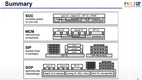
3. Summary: The Future of Chip Packaging
The past 15 years have transformed packaging from a protective shell into a performance multiplier. The table below compares these mainstream technologies.

Conclusion: As we move through 2026, the demand for AI computation and energy efficiency ensures that advanced packaging (CoWoS, SoIC, Foveros) will remain as critical as the lithography node itself. The goal remains constant: Improve functional density, shorten interconnects, and reduce power consumption.
 UTMEL
UTMEL
We are the professional distributor of electronic components, providing a large variety of products to save you a lot of time, effort, and cost with our efficient self-customized service. careful order preparation fast delivery service
1.What is IC packaging and testing?
In electronics manufacturing, integrated circuit packaging is the final stage of semiconductor device fabrication, in which the block of semiconductor material is encapsulated in a supporting case that prevents physical damage and corrosion. The packaging stage is followed by testing of the integrated circuit.
2.Why is IC packaging important?
IC packaging is the ability to provide more and more I/O interconnections to a die (bare chip) that is increasingly shrinking in size is an ever-present problem. This will imposes challenges for new 3D integration that requires innovative packaging technologies.
 Discovering New and Advanced Methodology for Determining the Dynamic Characterization of Wide Bandgap DevicesSaumitra Jagdale15 March 20242673
For a long era, silicon has stood out as the primary material for fabricating electronic devices due to its affordability, moderate efficiency, and performance capabilities. Despite its widespread use, silicon faces several limitations that render it unsuitable for applications involving high power and elevated temperatures. As technological advancements continue and the industry demands enhanced efficiency from devices, these limitations become increasingly vivid. In the quest for electronic devices that are more potent, efficient, and compact, wide bandgap materials are emerging as a dominant player. Their superiority over silicon in crucial aspects such as efficiency, higher junction temperatures, power density, thinner drift regions, and faster switching speeds positions them as the preferred materials for the future of power electronics.
Read More A Comprehensive Guide to FPGA Development BoardsUTMEL11 September 202520493
This comprehensive guide will take you on a journey through the fascinating world of FPGA development boards. We’ll explore what they are, how they differ from microcontrollers, and most importantly, how to choose the perfect board for your needs. Whether you’re a seasoned engineer or a curious hobbyist, prepare to unlock new possibilities in hardware design and accelerate your projects. We’ll cover everything from budget-friendly options to specialized boards for image processing, delve into popular learning paths, and even provide insights into essential software like Vivado. By the end of this article, you’ll have a clear roadmap to navigate the FPGA landscape and make informed decisions for your next groundbreaking endeavor.
Read More 800G Optical Transceivers: The Guide for AI Data CentersUTMEL24 December 202510801
The complete guide to 800G Optical Transceiver standards (QSFP-DD vs. OSFP). Overcome supply shortages and scale your AI data center with Utmel Electronic.
Read More The 2026 Engineer’s Guide: Choosing the Right MCU for Your Next IoT & New Energy ProjectUTMEL30 April 2026885
A comprehensive comparison of 2026's leading MCUs from ST, NXP, and Microchip across power efficiency, processing performance, connectivity, and ecosystems to help engineers select the optimal chip for next-gen IoT and new energy projects.
Read More AI Server Components: Engineering Next-Gen Data Center Hardware for 100kW RacksUTMEL15 May 2026426
The transition from traditional enterprise IT to AI-driven workloads has rendered legacy data center hardware obsolete, forcing infrastructure planners to re-engineer server components for extreme thermal environments.
Read More
Subscribe to Utmel !
![AT88SC25616C-PU]() AT88SC25616C-PU
AT88SC25616C-PUMicrochip Technology
![FM3164-G]() FM3164-G
FM3164-GCypress Semiconductor Corp
![HCS301-I/P]() HCS301-I/P
HCS301-I/PMicrochip Technology
![L9660TR]() L9660TR
L9660TRSTMicroelectronics
![MOC3062VM]() MOC3062VM
MOC3062VMON Semiconductor
![MOC3020SR2M]() MOC3020SR2M
MOC3020SR2MON Semiconductor
![FGBS3040E1-F085]() FGBS3040E1-F085
FGBS3040E1-F085ON Semiconductor
![ATSHA204-TSU-T]() ATSHA204-TSU-T
ATSHA204-TSU-TMicrochip Technology
![AD8196ACPZ]() AD8196ACPZ
AD8196ACPZAnalog Devices Inc.
![TLE8110EDXUMA1]() TLE8110EDXUMA1
TLE8110EDXUMA1Infineon Technologies


