Switching Power Supply Debugging: 10 Most Common Problems

HP Switching Power Supply Repair Part 2: Debugging the Startup Circuitry
Updated for 2025: As power electronics evolve with the adoption of GaN (Gallium Nitride) and SiC (Silicon Carbide) devices, the fundamental principles of topology troubleshooting remain critical. Below is a comprehensive guide to diagnosing common switching power supply (SMPS) failures, ranging from transformer saturation to startup glitches.
1. Transformer Saturation
The Phenomenon of Saturation
Transformer saturation occurs when the magnetic flux density in the core exceeds its maximum limit. When a transformer (or switching MOSFET) operates under high voltage input, heavy loading, capacitive loading, output short circuits, or extreme temperatures, the current flowing through the inductor can rise non-linearly.
In modern 2025 circuit designs, this is critical because once the core saturates, it effectively loses its inductance. The current acts as if it is flowing through a short circuit, becoming unpredictable and unregulated. This leads to immediate current overstress and can permanently damage the switching tube (MOSFET/IGBT) due to the resulting overvoltage spikes.
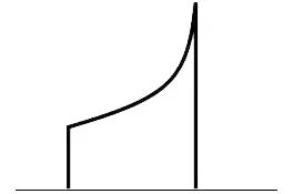
Figure 1: Current Waveform at Transformer Saturation
Common Causes:
The inductance of the transformer is designed too high.
The number of winding turns is insufficient (too few laps).
The saturation current rating of the transformer is lower than the maximum current limit (OCP) point of the control IC.
Absence of a proper soft-start mechanism.
Solutions:
Lower the current limiting threshold of the control IC.
Implement or strengthen the soft-start function. This ensures the current envelope rises gradually, preventing immediate saturation during startup.
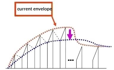
Figure 2: Current Envelope with Soft Start
2. Excessive Vds (Drain-Source Voltage) Stress
Design Requirements for Vds:
To ensure reliability in 2025 standards, the peak Vds value should not exceed 90% of the MOSFET's rated breakdown voltage even under worst-case scenarios (highest input voltage, heaviest load, extreme ambient temperature, or short-circuit conditions).
Methods to Reduce Vds:
1. Reduce the Reflected (Plateau) Voltage
Adjust the turns ratio between the primary and secondary windings. Reducing the primary turns relative to the secondary can lower the reflected voltage seen by the switch.
2. Suppress Voltage Spikes
Minimize Leakage Inductance: Leakage inductance stores energy that cannot be transferred to the secondary side, releasing it as a voltage spike when the switch turns off. Improving winding techniques (like sandwich winding) helps reduce this.
Optimize the Snubber/Clamp Circuit:
3. IC Overheating
Causes and Solutions:
1. High Internal MOSFET Losses
If the internal switching losses are too high, or the transformer's parasitic capacitance causes a large crossover area between the MOSFET's turn-on/turn-off current and Vds, the IC will overheat.
Fix: Increase the distance between transformer windings or use insulating tape layers to reduce interlayer parasitic capacitance.
2. Poor Thermal Dissipation
The IC relies on its pins and the connected PCB copper foil to dissipate heat.
Fix: Increase the amount of solder on ground pins and expand the area of the connected copper foil (ground plane) to act as a heatsink.
3. High Ambient Temperature
Fix: Ensure the IC is located in an area with adequate airflow and kept away from other high-heat components (like transformers or power resistors).
4. Failure to Start at No-Load or Light-Load
Phenomenon:
The power supply fails to start under light or no-load conditions. The Vcc pin voltage oscillates repeatedly between the startup threshold and the shutdown (UVLO) voltage.
Reason:
Under light loads, the switching frequency or duty cycle drops, causing the induced voltage on the auxiliary Vcc winding to fall below the level needed to sustain the IC operation.
Solution:
Increase the number of turns on the Vcc auxiliary winding to boost voltage generation. Alternatively, lower the Vcc current-limiting resistor or add a small dummy load. Note: If Vcc becomes too high under heavy loads after these changes, a linear regulator or clamping circuit may be needed to stabilize it.
5. Shutdown Upon Reloading (Heavy Load)
Causes and Solutions:
1. Vcc Overvoltage Protection (OVP)
When a heavy load is applied, the induced voltage on the Vcc winding increases significantly. If it hits the IC's OVP threshold, the controller shuts down to prevent damage.
2. Internal Current Limit Triggered
Current Limit Set Too Low: If the current limit point is too restrictive, the MOSFET cannot conduct enough current to drive the heavy load, causing output voltage droop. Fix: Adjust the current-sensing resistor (Rsense) to raise the limit.
Steep Current Slope: If the inductor current rises too steeply (low inductance), it hits the current limit prematurely. Fix: Increase the transformer inductance (without reaching saturation limits).
6. High Standby Input Power
Phenomenon:
The power supply consumes excessive power in standby mode, and output ripple is high.
Reason:
This often occurs if the Vcc is unstable, forcing the IC into a restart loop (consuming high voltage startup current repeatedly). Additionally, if the startup resistor is continuously connected to high voltage, it wastes power.
Furthermore, if the controller fails to enter Burst Mode (or "skip cycle" mode) effectively, switching losses remain high even with no load.
Solution:
Optimize the feedback network parameters to allow the controller to enter deep Burst Mode at light loads, reducing the effective switching frequency.
7. Excessive Short-Circuit Power Consumption
Phenomenon:
When the output is short-circuited, input power consumption spikes, and Vds stress becomes dangerous.
Mechanism:
During a short circuit, the switch may continue to fire chaotic pulses. Because the leakage inductance energy cannot be delivered to the load, it dumps back into the switch, causing high voltage stress.
Solutions:
Faster OCP Response: Reduce the capacitance on the feedback pin so the Over Current Protection triggers faster. This immediately halts switching action when a short occurs.
Duty Cycle Clamping: Ensure the IC enters a low-frequency "hiccup mode" during shorts to minimize average power dissipation.
8. High Output Ripple at Light Load
Phenomenon:
The output voltage fluctuates significantly (high ripple) during no-load or light-load operation.
Reason:
If the oscillator or controller operates intermittently at a very low frequency (Burst Mode), the period between energy packets may be too long. This causes the output capacitor to discharge too much between cycles.
Solution:
While maintaining standby power requirements, slightly increase the minimum burst frequency or increase the output capacitance to hold charge longer between switching cycles.
9. Failure to Start with Capacitive Loads
The Challenge:
The power supply starts fine with a resistor but fails when connected to a large capacitive load (e.g., >10,000µF). Modern 2025 specifications often require the voltage to stabilize within 20ms.
Formula: Energy $E = 0.5 \times C \times V^2$. A large capacitor requires significant energy transfer in a short time.
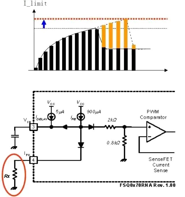
Figure 3: Legacy Chip Example (FSQ0170RNA)
Solutions (Classic Topology Analysis):
1. Increase Peak Current Limit
Adjust the current sensing on the comparator or feedback pin to allow a higher peak current (Id) through the MOSFET. This transfers more energy per cycle during startup.
2. Extend Feedback (Vfb) Rise Time
The Over Current Protection (OCP) is often triggered when the feedback voltage ($V_{fb}$) hits a ceiling (e.g., 6V). If the output capacitor takes too long to charge, $V_{fb}$ maxes out, and the IC shuts down.

Figure 4: Extending the Rise Time of Feedback Voltage ($V_{fb}$)
Technical Fixes:
Increase Feedback Capacitor (C9): This slows the rise of $V_{fb}$, giving the output voltage more time to reach regulation before the protection trips. Warning: Too large a capacitor will slow down transient response.
Soft-Start Capacitor (C7): Place a capacitor in series with a Zener diode across the feedback pin. This delays the voltage rise only during startup without affecting steady-state loop response.
10. Output Voltage Bounce (Restart Loop)
Phenomenon:
After unplugging the input power, the output voltage drops but then momentarily "bounces" or spikes back up before dying completely.
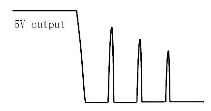
Figure 5: Voltage Bounce Waveform
Reason:
Even after AC power is cut, the large bulk capacitor on the primary side holds a charge. If the IC turns off due to low Vcc but the bulk voltage is still high enough to push current through the startup resistor, the IC may attempt a "zombie" restart, causing the output to glitch.
Solution:
Ensure the IC hits its UVLO (Under Voltage Lockout) completely. Increase the value of the startup resistor so that as the bulk capacitor voltage drops, it can no longer supply enough current to restart the IC. Alternatively, use an X-capacitor discharge resistor to drain the input faster.
1. What waveforms should switching power supply design and debugging should look at?
PWM frequency and duty cycle, inductor current waveform (know Ipeak and ripple rate), output voltage waveform (know output DC and ripple), switch current (know whether switch power loss and switching frequency parameters are appropriate).
2. How to Test Waveforms in Switching Power Supplies?
The low-voltage part is directly tested with a probe, and the high-voltage part is tested by unplugging the ground wire of the power plug of the oscilloscope.
3. How to test the working frequency of switching power supply?
Measure the secondary waveform, calculate after stabilization, and the digital oscilloscope displays the frequency directly.
 LLC Converter with Planar Matrix Transformer for High-Current-High-Power ApplicationsSaumitra Jagdale15 March 20244388
The rise of data centres in recent years, driven by cloud computing and big data, has caused a significant increase in electricity consumption. In the United States alone, it exceeded 70 billion kWh by 2014, making up 1.8% of total national electricity usage.
Read More Enhancing Frequency Stability in Modern Distributed Power SystemsRakesh Kumar, Ph.D.21 September 20243945
The article discusses the importance of primary frequency regulation in maintaining grid stability. It also explores battery energy storage systems, virtual synchronous generators, and advanced control strategies to enhance frequency stability in power systems.
Read More The Impact of SMPS on LED Lighting and Diverse IndustriesUTMEL05 June 20252283
Switched-Mode Power Supplies (SMPS) enhance LED lighting and industries by improving energy efficiency, reliability, and sustainability across diverse applications.
Read More What is Uninterruptible Power Supply (UPS)?UTMEL08 April 20214937
UPS is an uninterruptible power supply containing the energy storage device. It is mainly used to give a part of a device with a higher power stability, providing uninterrupted power supplies.
Read More Switch-mode Power Supply BasicsUTMEL14 December 20207524
Switched-mode Power Supply (SMPS), also known as switching converter, is a high-frequency electric energy conversion device and a type of power supply. Its function is to convert a level of voltage into the voltage or current required by the user through different forms of architecture.
Read More
Subscribe to Utmel !
![34.51.7.005.0010]() 34.51.7.005.0010
34.51.7.005.0010Finder Relays, Inc.
![DRC3P48D420]() DRC3P48D420
DRC3P48D420Sensata-Crydom
![LKT1AF-24V]() LKT1AF-24V
LKT1AF-24VPanasonic Electric Works
![JW2ASN-DC24V]() JW2ASN-DC24V
JW2ASN-DC24VPanasonic Electric Works
![SZR-LY2-1-AC24V]() SZR-LY2-1-AC24V
SZR-LY2-1-AC24VHoneywell Sensing and Productivity Solutions
![LY4-DC6]() LY4-DC6
LY4-DC6Omron Automation and Safety
![NC4D-P-DC24V]() NC4D-P-DC24V
NC4D-P-DC24VPanasonic Electric Works
![ALD112]() ALD112
ALD112Panasonic Electric Works
![DK1A-3V-F]() DK1A-3V-F
DK1A-3V-FPanasonic Electric Works
![DSP1A-L2-DC9V]() DSP1A-L2-DC9V
DSP1A-L2-DC9VPanasonic Electric Works


 Product
 Brand
Brand Articles
 Tools
Tools


