Using SiC-GaN to Create Two-Phase Interleaved DC-DC Converters for Plug-in Electric Vehicles
| Topics covered in this article: |
| Ⅰ. Mathematical calculation of models |
| Ⅱ. Results after simulation |
| Ⅲ. Conclusion |
The demand for electric vehicles is increasing day by day, mainly due to declining fossil fuel reserves. Moreover, it is economical to choose electric vehicles, as it requires less running cost with no damage to the environment. Considering these facts, it is logical to improve the efficiency of batteries and components. One of the ways to do so is by using Wide Band Gap, Gallium Nitride, and Silicon Carbide over Silicon in power converters as traditional DC-DC converters contribute to massive power losses.
It has recently come to light that GaN transistors are more efficient due to lower switching power loss as compared to SiC. Since power density is vital for universal DC-DC converters, power electronic converters in PEVs, and commercial GaN transistors with lateral structures cannot be used as they have high power limitations.
With the use of a universal converter, the number of modules used will decrease which in turn will increase power density and reliability helping us improve the efficiency and design of PEVs. In order to tackle the limitation of the lateral GaN transistors, a multiphase topology can be used for the application of a universal dc-dc converter in PEVs. However, this comes with its own set of issues. The obstacle is that a multi-phase converter with an elevated number of phases is not applicable to power electronics.
To tackle these issues, a new two-phase interleaved bidirectional boost converter is examined, in which one phase is GaN-based whereas the other phase is SiC-based. The principle behind it is to use the GaN-based phase only for power conversion in the range of 1-15Kw. The other phase provides conversion for more than 15kw of power.
Modern applications like multi-input and zero-voltage switching use multi-phase topology to share current between two phases, this same technology is used in the power converter. However, unlike other converters, this proposed design uses active devices of different types. The configuration of the converter is shown in figure 1.

Figure.1 SiC-GaN-based converter layout
One might think that as this configuration has mismatched current sharing, the diode with a higher current will have a higher temperature which will ultimately cause instability. Although this is not true because of bidirectional topology, both sides of the converter are transistors. Moreover, as there is no need for body and anti-parallel diodes, this technology proves to be a huge advancement.
In order to design the inductor, it is important to consider the converter conduction mode which in this case is set to be continuous. Considering this, the amount of inductor can be calculated as shown in equation 1:

Equation 1
Here, Vo is the dc bus voltage, Vin is the battery voltage, ݂fs is the switching frequency, and IL(min) is the minimum inductor currents. As minimum current is supplied only by the GaN phase, there was no advantage of a small inductor size when compared to a single-phase converter. Concurrently, the high voltage capacitor can be calculated as shown in equation 2:

Equation 2
Ⅰ. Mathematical calculation of models
We investigate the intervals to obtain the converter's mathematical model. Hence, we analyze the boost mode in which a voltage ration equivalent to 2 is required (Vin = 300 [V] and Vo = 600 [V]). the duty cycle of the boost converter and its voltage ratio are given below as follows:

Equation 3
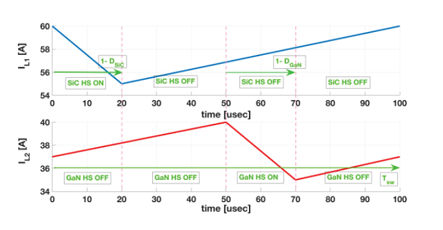
In the above equation, η is the efficiency of the converter. As efficiency is always less than 1, the duty cycle of the converter is greater than 50 percent. On the other side, the switching commands in an interleaved two-phase converter have a time shift of T/2 where T = 1/fs is the time period. Taking into account, the possible inductor currents are shown below:

Figure.2 Inductor currents
In the above figure, there are three intervals for the converter:

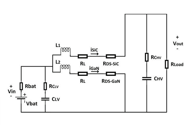
Figure.3 First interval topology
1) The High side (HS) SiC is on and HS GaN is off in fig 3 above where the L1 current is discharged through the HS SiC and the output load, L2 current is charging through the low side (LS) GaN.

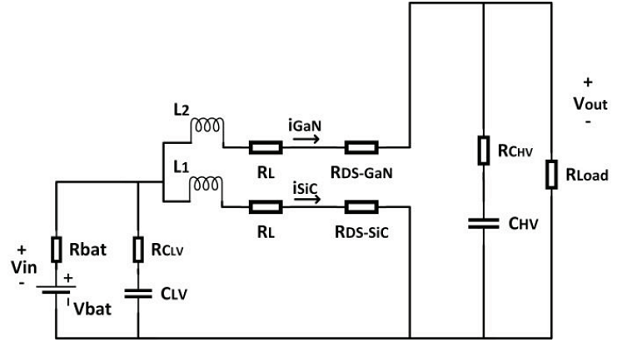
Figure.4 Second interval topology
2) In HS SiC is off and in HS GaN is on shown in Fig 4 where the L1 current is charging through LS SiC and L2 current is discharging through HS GaN and the output load.

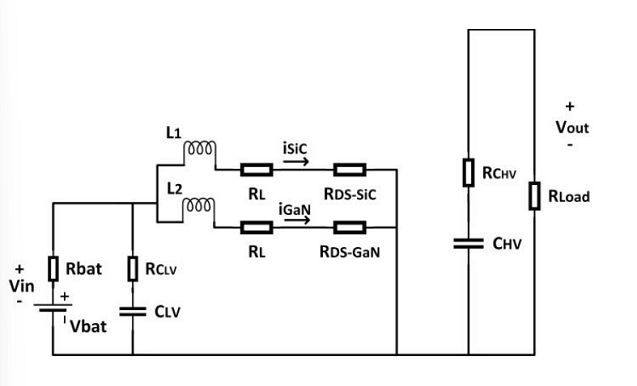
Figure.5 Third interval topology
3) Together HS SiC and HS GaN are off in Fig 5 in which L1 is charged through LS SiC and L2 current is charged through LS GaN.
Ⅱ. Results after simulation
To investigate the power losses and efficiency of the converter, spiced-based simulations are executed. There are various methods to calculate power losses like using data from spice-based simulations or using the datasheet of the device. In this research, this method is an analytical combination of both the mentioned methods.
For example, to calculate the switching losses, the values of turn-on and turn-off switching times are observed from the simulations; when calculating conduction loss, reverse recovery loss, and gate loss the values of RDS(on), Qrr, and Qg(tot) are achieved from the datasheet of the transistor.
A. Switching Loss:

Equation 4
When compared with SiC the amounts of Ton and Toff are lesser for GaN and hence GaN devices tend to have more minor power switching losses.
B. Conduction Loss:

Equation 5
In the above equation, D is the duty cycle of the respective device. As the efficiency of the proposed converter is greater than the two-phased SiC-based converter, hence the main contributor to the power losses in switching loss.
C. Reverse Recovery Loss:

Equation 6
Here Qrr is the device's body diode reverse recovery charge. As Qrr is zero for GaN devices, it is not a big drawback as compared to switching loss.
Ⅲ. Conclusion
An experiment was conducted to test a new dc-dc converter for a universally accepted dc-dc power system in the EV industry. By using GaN transistors, multiple complications with concerns to the multi-phase converters were smoothly avoided and all operational objectives were achieved successfully. To ensure this, researchers conducted a power loss analysis where the proposed converter was compared to a SiC-based converter.
The simulation results proved to demonstrate a higher and more balanced efficiency as compared to the SiC-based converter. In the range of 5-40 KW, the proposed converter demonstrated maximum efficiency at low, medium, and full loads.
 MOSFET vs. IGBT: Characteristics, Structure and Market AnalysisUTMEL25 December 202521966
With the rise of new energy in recent years, the market demand for MOSFETs and IGBTs is increasing steeply. Generally used as switching devices, they are widely used in electronic circuits. MOSFETs and IGBTs are relatively similar in appearance and characteristics parameters. So what is the difference between MOSFETs and IGBTs?
Read More Introduction to FinFETUTMEL18 March 202129503
The full name of FinFET is Fin Field-Effect Transistor. It is a new complementary metal oxide semiconductor transistor. The FinFET name is based on the similarity between the shape of the transistor and the fin.
Read More What is a MOSFET?UTMEL16 April 20217215
MOSFET, short for Metal-Oxide-Semiconductor Field-Effect Transistor, is a field-effect transistor that can be widely used in analog circuits and digital circuits. MOSFETs can be divided into N-channel type with the majority of electrons and P-channel type with the majority of holes according to their "channel" polarity. They are usually called NMOSFET and PMOSFET.
Read More NPN Transistors and PNP TransistorsUTMEL29 October 20209461
NPN and PNP are two types of transistors. Transistors are semiconductor devices made of doped p-type and n-type junctions. This article mainly introduces the differences between this two kinds of transistors, the methods of distinguishing them, and the application of them.
Read More An Overview of Bipolar TransistorsUTMEL27 August 20208689
Bipolar Transistor, full name bipolar junction transistor(BJT), is an electronic device with three terminals, made of three parts of semiconductors with different levels of doping. The charge flow in the transistor is mainly due to the diffusion and drift movement of carriers at the PN junction.
Read More
Subscribe to Utmel !
![82635AWGDVKPRQ]() 82635AWGDVKPRQ
82635AWGDVKPRQIntel RealSense
![BLM02AX241SN1D]() BLM02AX241SN1D
BLM02AX241SN1DMurata Electronics
![URAM3C21]() URAM3C21
URAM3C21Vicor Corporation
![BR24L16F-WE2]() BR24L16F-WE2
BR24L16F-WE2ROHM Semiconductor
![BLM03BB121SN1D]() BLM03BB121SN1D
BLM03BB121SN1DMurata Electronics
![BLM18PG471SH1D]() BLM18PG471SH1D
BLM18PG471SH1DMurata Electronics
![1D15F1500]() 1D15F1500
1D15F1500APEM Inc.
![REC20-25-201-1]() REC20-25-201-1
REC20-25-201-1Nidec Copal Electronics
![JW2SN-DC12V]() JW2SN-DC12V
JW2SN-DC12VPanasonic Electric Works
![1427G]() 1427G
1427GHammond Manufacturing


 Product
 Brand
Brand Articles
 Tools
Tools


