
 Product
 Brand
Brand Articles
 Tools
Tools
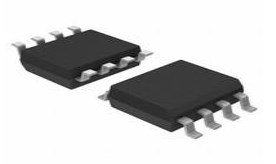
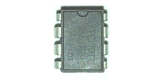
AD7091R-2 SAR ADC: Pinout, Features and Datasheet


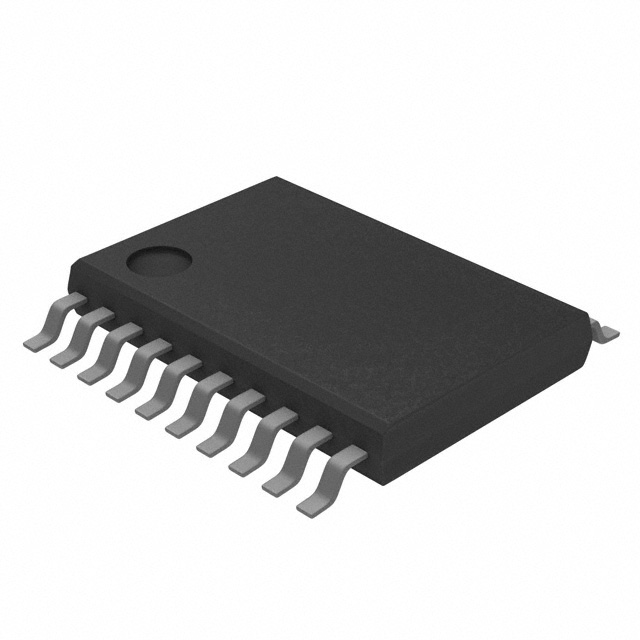
12 Bit 0.65mm ADC AD7091 3V 16-TSSOP (0.173, 4.40mm Width)
The AD7091R-2 is a multichannel 12-bit, ultralow power, successive approximation analog-to-digital converter (ADC) that is available in two analog input channel options. The AD7091R-2 is capable of throughput rates of 1 MSPS. Furthermore, Huge range of Semiconductors, Capacitors, Resistors and IcS in stock. Welcome RFQ.

Introduction to ADC and DAC
AD7091R-2 Pinout

Pinout
AD7091R-2 CAD Model

PCB Symbol

PCB Footprint

3D Model
AD7091R-2 Overview
The AD7091R-2 is a multichannel 12-bit, ultralow power, successive approximation analog-to-digital converter (ADC) that is available in two analog input channel options. The AD7091R-2 operates from a single 2.7 V to 5.25 V power supply and are capable of achieving a sampling rate of 1 MSPS. The AD7091R-2 offers up to eight single-ended analog input channels with a channel sequencer that allows a preprogrammed selection of channels to be converted sequentially. The AD7091R-2 also features an on-chip conversion clock, an on-chip accurate 2.5 V reference, and a high speed serial interface. The AD7091R-2 has a serial port interface (SPI) that allows data to be read after the conversion while achieving a 1 MSPS throughput rate. The AD7091R-2 uses advanced design techniques to achieve ultralow power dissipation at high throughput rates. It also features flexible power management options. An on-chip configuration register allows the user to set up different operating conditions. These include power management, alert functionality, busy indication, channel sequencing, and general-purpose output pins. The MUXOUT and ADCIN pins allow signal conditioning of the multiplexer output prior to acquisition by the ADC.
This article provides you with a basic overview of the AD7091R-2 SAR ADC, including its pin descriptions, features and specifications, etc., to help you quickly understand what AD7091R-2 is.
AD7091R-2 Features
● Ultralow system power
◆ Flexible power/throughput rate management
◆ Normal mode
▼ 1.4 mW at 1 MSPS
◆ Power-down mode
▼ 550 nA typical at VDD = 5.25 V
▼ 435 nA typical at VDD = 3 V
● High performance
◆ 1 MSPS throughput with no latency/pipeline delay
◆ SNR: 70 dB typical at 10 kHz input frequency
◆ THD: −80 dB typical at 10 kHz input frequency
◆ INL: ±0.7 LSB typical, ±1.0 LSB maximum
● Small system footprint
◆ On-chip accurate 2.5 V reference, 5 ppm/°C typical drift
◆ MUXOUT/ADCIN to allow single buffer amplifier
◆ Daisy-chain mode
◆ 16-lead TSSOP package
● Easy to use
◆ SPI/QSPI™/MICROWIRE™/DSP compatible digital interface
◆ Integrated programmable channel sequencer
● Built in features for control and monitoring applications
● Wide operating range
◆ Temperature range: −40°C to +125°C
◆ Specified for VDD of 2.7 V to 5.25 V
Specifications
- TypeParameter
- Lifecycle Status
Lifecycle Status refers to the current stage of an electronic component in its product life cycle, indicating whether it is active, obsolete, or transitioning between these states. An active status means the component is in production and available for purchase. An obsolete status indicates that the component is no longer being manufactured or supported, and manufacturers typically provide a limited time frame for support. Understanding the lifecycle status is crucial for design engineers to ensure continuity and reliability in their projects.
PRODUCTION (Last Updated: 1 month ago) - Factory Lead Time8 Weeks
- Mount
In electronic components, the term "Mount" typically refers to the method or process of physically attaching or fixing a component onto a circuit board or other electronic device. This can involve soldering, adhesive bonding, or other techniques to secure the component in place. The mounting process is crucial for ensuring proper electrical connections and mechanical stability within the electronic system. Different components may have specific mounting requirements based on their size, shape, and function, and manufacturers provide guidelines for proper mounting procedures to ensure optimal performance and reliability of the electronic device.
Surface Mount - Mounting Type
The "Mounting Type" in electronic components refers to the method used to attach or connect a component to a circuit board or other substrate, such as through-hole, surface-mount, or panel mount.
Surface Mount - Package / Case
refers to the protective housing that encases an electronic component, providing mechanical support, electrical connections, and thermal management.
16-TSSOP (0.173, 4.40mm Width) - Number of Pins16
- Operating Temperature
The operating temperature is the range of ambient temperature within which a power supply, or any other electrical equipment, operate in. This ranges from a minimum operating temperature, to a peak or maximum operating temperature, outside which, the power supply may fail.
-40°C~125°C - Packaging
Semiconductor package is a carrier / shell used to contain and cover one or more semiconductor components or integrated circuits. The material of the shell can be metal, plastic, glass or ceramic.
Tube - JESD-609 Code
The "JESD-609 Code" in electronic components refers to a standardized marking code that indicates the lead-free solder composition and finish of electronic components for compliance with environmental regulations.
e3 - Pbfree Code
The "Pbfree Code" parameter in electronic components refers to the code or marking used to indicate that the component is lead-free. Lead (Pb) is a toxic substance that has been widely used in electronic components for many years, but due to environmental concerns, there has been a shift towards lead-free alternatives. The Pbfree Code helps manufacturers and users easily identify components that do not contain lead, ensuring compliance with regulations and promoting environmentally friendly practices. It is important to pay attention to the Pbfree Code when selecting electronic components to ensure they meet the necessary requirements for lead-free applications.
no - Part Status
Parts can have many statuses as they progress through the configuration, analysis, review, and approval stages.
Active - Moisture Sensitivity Level (MSL)
Moisture Sensitivity Level (MSL) is a standardized rating that indicates the susceptibility of electronic components, particularly semiconductors, to moisture-induced damage during storage and the soldering process, defining the allowable exposure time to ambient conditions before they require special handling or baking to prevent failures
2 (1 Year) - Number of Terminations16
- ECCN Code
An ECCN (Export Control Classification Number) is an alphanumeric code used by the U.S. Bureau of Industry and Security to identify and categorize electronic components and other dual-use items that may require an export license based on their technical characteristics and potential for military use.
EAR99 - Terminal Finish
Terminal Finish refers to the surface treatment applied to the terminals or leads of electronic components to enhance their performance and longevity. It can improve solderability, corrosion resistance, and overall reliability of the connection in electronic assemblies. Common finishes include nickel, gold, and tin, each possessing distinct properties suitable for various applications. The choice of terminal finish can significantly impact the durability and effectiveness of electronic devices.
Matte Tin (Sn) - Max Power Dissipation
The maximum power that the MOSFET can dissipate continuously under the specified thermal conditions.
3.4mW - Terminal Position
In electronic components, the term "Terminal Position" refers to the physical location of the connection points on the component where external electrical connections can be made. These connection points, known as terminals, are typically used to attach wires, leads, or other components to the main body of the electronic component. The terminal position is important for ensuring proper connectivity and functionality of the component within a circuit. It is often specified in technical datasheets or component specifications to help designers and engineers understand how to properly integrate the component into their circuit designs.
DUAL - Terminal Form
Occurring at or forming the end of a series, succession, or the like; closing; concluding.
GULL WING - Peak Reflow Temperature (Cel)
Peak Reflow Temperature (Cel) is a parameter that specifies the maximum temperature at which an electronic component can be exposed during the reflow soldering process. Reflow soldering is a common method used to attach electronic components to a circuit board. The Peak Reflow Temperature is crucial because it ensures that the component is not damaged or degraded during the soldering process. Exceeding the specified Peak Reflow Temperature can lead to issues such as component failure, reduced performance, or even permanent damage to the component. It is important for manufacturers and assemblers to adhere to the recommended Peak Reflow Temperature to ensure the reliability and functionality of the electronic components.
260 - Number of Functions1
- Supply Voltage
Supply voltage refers to the electrical potential difference provided to an electronic component or circuit. It is crucial for the proper operation of devices, as it powers their functions and determines performance characteristics. The supply voltage must be within specified limits to ensure reliability and prevent damage to components. Different electronic devices have specific supply voltage requirements, which can vary widely depending on their design and intended application.
3V - Terminal Pitch
The center distance from one pole to the next.
0.65mm - Time@Peak Reflow Temperature-Max (s)
Time@Peak Reflow Temperature-Max (s) refers to the maximum duration that an electronic component can be exposed to the peak reflow temperature during the soldering process, which is crucial for ensuring reliable solder joint formation without damaging the component.
30 - Base Part Number
The "Base Part Number" (BPN) in electronic components serves a similar purpose to the "Base Product Number." It refers to the primary identifier for a component that captures the essential characteristics shared by a group of similar components. The BPN provides a fundamental way to reference a family or series of components without specifying all the variations and specific details.
AD7091 - Pin Count
a count of all of the component leads (or pins)
16 - Polarity
In electronic components, polarity refers to the orientation or direction in which the component must be connected in a circuit to function properly. Components such as diodes, capacitors, and LEDs have polarity markings to indicate which terminal should be connected to the positive or negative side of the circuit. Connecting a component with incorrect polarity can lead to malfunction or damage. It is important to pay attention to polarity markings and follow the manufacturer's instructions to ensure proper operation of electronic components.
Unipolar - Configuration
The parameter "Configuration" in electronic components refers to the specific arrangement or setup of the components within a circuit or system. It encompasses how individual elements are interconnected and their physical layout. Configuration can affect the functionality, performance, and efficiency of the electronic system, and may influence factors such as signal flow, impedance, and power distribution. Understanding the configuration is essential for design, troubleshooting, and optimizing electronic devices.
S/H-ADC - Interface
In electronic components, the term "Interface" refers to the point at which two different systems, devices, or components connect and interact with each other. It can involve physical connections such as ports, connectors, or cables, as well as communication protocols and standards that facilitate the exchange of data or signals between the connected entities. The interface serves as a bridge that enables seamless communication and interoperability between different parts of a system or between different systems altogether. Designing a reliable and efficient interface is crucial in ensuring proper functionality and performance of electronic components and systems.
SPI - Max Supply Voltage
In general, the absolute maximum common-mode voltage is VEE-0.3V and VCC+0.3V, but for products without a protection element at the VCC side, voltages up to the absolute maximum rated supply voltage (i.e. VEE+36V) can be supplied, regardless of supply voltage.
5.25V - Min Supply Voltage
The minimum supply voltage (V min ) is explored for sequential logic circuits by statistically simulating the impact of within-die process variations and gate-dielectric soft breakdown on data retention and hold time.
2.7V - Operating Supply Current
Operating Supply Current, also known as supply current or quiescent current, is a crucial parameter in electronic components that indicates the amount of current required for the device to operate under normal conditions. It represents the current drawn by the component from the power supply while it is functioning. This parameter is important for determining the power consumption of the component and is typically specified in datasheets to help designers calculate the overall power requirements of their circuits. Understanding the operating supply current is essential for ensuring proper functionality and efficiency of electronic systems.
500μA - Nominal Supply Current
Nominal current is the same as the rated current. It is the current drawn by the motor while delivering rated mechanical output at its shaft.
349μA - Power Dissipation
the process by which an electronic or electrical device produces heat (energy loss or waste) as an undesirable derivative of its primary action.
1mW - Number of Bits12
- Input Type
Input type in electronic components refers to the classification of the signal or data that a component can accept for processing or conversion. It indicates whether the input is analog, digital, or a specific format such as TTL or CMOS. Understanding input type is crucial for ensuring compatibility between different electronic devices and circuits, as it determines how signals are interpreted and interacted with.
Single Ended - Min Input Voltage
The parameter "Min Input Voltage" in electronic components refers to the minimum voltage level that must be applied to the component for it to operate within its specified parameters. This value is crucial as providing a voltage below this minimum threshold may result in the component malfunctioning or not functioning at all. It is important to adhere to the specified minimum input voltage to ensure the proper operation and longevity of the electronic component. Failure to meet this requirement may lead to potential damage to the component or the overall system in which it is used.
1V - Architecture
In electronic components, the parameter "Architecture" refers to the overall design and structure of the component. It encompasses the arrangement of internal components, the layout of circuitry, and the physical form of the component. The architecture of an electronic component plays a crucial role in determining its functionality, performance, and compatibility with other components in a system. Different architectures can result in variations in power consumption, speed, size, and other key characteristics of the component. Designers often consider the architecture of electronic components carefully to ensure optimal performance and integration within a larger system.
SAR - Number of Inputs1
- Max Input Voltage
Max Input Voltage refers to the maximum voltage level that an electronic component can safely handle without getting damaged. This parameter is crucial for ensuring the proper functioning and longevity of the component. Exceeding the specified maximum input voltage can lead to overheating, electrical breakdown, or permanent damage to the component. It is important to carefully adhere to the manufacturer's guidelines regarding the maximum input voltage to prevent any potential issues and maintain the reliability of the electronic device.
5.25V - Converter Type
The parameter "Converter Type" in electronic components refers to the classification of devices that convert one form of energy or signal to another. This includes devices such as analog-to-digital converters (ADCs), digital-to-analog converters (DACs), and various types of signal converters used in communication, power management, and measurement systems. Each converter type is designed to facilitate the manipulation or transformation of signals to meet specific application requirements. The choice of converter type typically depends on factors such as the signal characteristics, required accuracy, and conversion speed.
ADC, SUCCESSIVE APPROXIMATION - Supply Type
Supply Type in electronic components refers to the classification of power sources used to operate the component. It indicates whether the component requires DC or AC power, and if DC, specifies the voltage levels such as low, medium, or high. Different supply types can affect the performance, compatibility, and application of the component in electronic circuits. Understanding the supply type is crucial for proper component selection and integration into electronic designs.
Single - Reference Type
a code object that is not stored directly where it is created, but that acts as a kind of pointer to a value stored elsewhere.
Supply - Data Interface
A Data Interface in EDQ is a template of a set of attributes representing a given entity, used to create processes that read from, or write to, interfaces rather than directly from or to sources or targets of data.
SPI, DSP - Resolution
Resolution in electronic components refers to the smallest increment of measurement or change that can be detected or represented by the component. It is a crucial specification in devices such as sensors, displays, and converters, as it determines the level of detail or accuracy that can be achieved. For example, in a digital camera, resolution refers to the number of pixels that make up an image, with higher resolution indicating a greater level of detail. In analog-to-digital converters, resolution is the number of discrete values that can be represented in the digital output, determining the precision of the conversion process. Overall, resolution plays a significant role in determining the performance and capabilities of electronic components in various applications.
1.5 B - Sampling Rate
often described in the context of signal processing as the number of samples per time.
1 Msps - Voltage - Supply, Analog
Voltage - Supply, Analog is a parameter in electronic components that specifies the range of voltage levels required to power the analog circuitry within the component. This parameter indicates the minimum and maximum voltage levels that the component can accept for proper operation of its analog functions. It is crucial to ensure that the voltage supplied to the component falls within this specified range to prevent damage and ensure optimal performance. Understanding and adhering to the "Voltage - Supply, Analog" parameter is essential for the proper functioning of analog circuits in electronic components.
2.09V~5.25V - Voltage - Supply, Digital
Voltage - Supply, Digital is a parameter that specifies the voltage level required to power the digital circuitry within an electronic component, such as an integrated circuit or a microcontroller. This parameter is crucial for ensuring proper operation of the digital components, as supplying the correct voltage level is essential for reliable performance. The specified voltage range typically includes both minimum and maximum values within which the component can operate safely and efficiently. It is important to adhere to the recommended voltage supply range to prevent damage to the component and to maintain the integrity of the digital signals being processed.
2.09V~5.25V - Number of Analog In Channels2
- Sampling Rate (Per Second)
The sampling rate (per second) in electronic components refers to the frequency at which an analog signal is measured or sampled to convert it into a digital signal. It is typically expressed in Hertz (Hz) and indicates how many times per second the analog signal is sampled. A higher sampling rate allows for better representation of the original signal, capturing more detail and reducing distortion during the conversion process. In audio applications, for example, common sampling rates include 44.1 kHz for CD-quality audio and 48 kHz for video production.
1M - Output Bit Code
Output Bit Code refers to the digital representation of the output signal of an electronic component, typically in binary form. It indicates the specific combination of bits that represent the output value of the component. The output bit code is crucial for interpreting and processing the output data accurately in digital systems. By understanding the output bit code, engineers can design appropriate circuits and algorithms to manipulate and utilize the output information effectively.
BINARY - Integral Nonlinearity (INL)
Integral Nonlinearity (INL) is a measure of the deviation of a transfer function from a straight line when considering the entire output range of a device, such as a digital-to-analog converter or an analog-to-digital converter. It is quantified as the maximum deviation of the actual output from the ideal output across the entire input range, expressed as a percentage of the full-scale output. INL indicates how closely the output follows a linear model, influencing the accuracy of the signal representation in electronic components. A lower INL value signifies better linearity and higher precision in signal processing applications.
1.25 LSB - Sample and Hold / Track and Hold
"Sample and Hold" and "Track and Hold" are two related functions commonly found in electronic components such as analog-to-digital converters (ADCs) and signal processing circuits. In a Sample and Hold circuit, the input signal is sampled at specific intervals and held constant until the next sampling period. This allows the circuit to capture and store the input signal's value for further processing or conversion.On the other hand, a Track and Hold circuit continuously tracks the input signal's value and holds it steady when required, typically during the conversion process. This ensures that the input signal remains constant and accurate during the conversion process.Both functions are essential in maintaining the integrity and accuracy of analog signals in digital systems, allowing for precise measurements and processing of signals in various electronic applications.
TRACK - Input Capacitance
The capacitance between the input terminals of an op amp with either input grounded. It is expressed in units of farads.
10pF - Ratio - S/H:ADC
The parameter "Ratio - S/H:ADC" in electronic components refers to the ratio between the sample and hold (S/H) circuit and the analog-to-digital converter (ADC) in a system. The sample and hold circuit is responsible for capturing and holding the input signal at a specific moment in time, while the ADC converts this analog signal into a digital format for processing. The ratio between the S/H and ADC components is important as it determines the accuracy and speed of the analog-to-digital conversion process. A higher ratio typically indicates a more precise and efficient conversion process, leading to better overall performance of the electronic system. Engineers often consider this parameter when designing and optimizing electronic circuits to ensure reliable and high-quality signal processing.
1:1 - Output Format
Output formats are used to determine which data is exported and how data is displayed in many areas of OLIB.
SERIAL - Signal to Noise Ratio (SNR)
Signal to Noise Ratio (SNR) is a measure used in electronics to quantify the ratio of the strength of a desired signal to the strength of background noise. It is commonly expressed in decibels (dB) and is used to evaluate the quality of a signal transmission or processing system. A higher SNR indicates a stronger, clearer signal relative to the background noise, resulting in better performance and accuracy in electronic components such as amplifiers, receivers, and communication systems. SNR is crucial in ensuring reliable and efficient operation of electronic devices by minimizing the impact of unwanted noise on the signal quality.
70 dB - Differential Nonlinearity
Differential Nonlinearity (DNL) is a parameter used to measure the deviation of the actual step size between two adjacent digital output codes in an analog-to-digital converter (ADC) or digital-to-analog converter (DAC) from the ideal step size. It quantifies the accuracy of the converter in maintaining consistent step sizes across the entire range of digital codes. DNL is typically expressed in terms of least significant bits (LSBs) and is an important factor in determining the overall performance and linearity of the converter. A lower DNL value indicates better linearity and accuracy in the conversion process, while a higher DNL value suggests potential errors and nonlinearity in the output signal.
0.9 LSB - Conversion Time-Max
Conversion Time-Max is a parameter in electronic components that refers to the maximum amount of time it takes for a device to complete a conversion process. This parameter is commonly found in analog-to-digital converters (ADCs) and digital-to-analog converters (DACs). It is an important specification as it determines the speed at which the device can convert an analog signal into a digital format or vice versa. A shorter conversion time-max indicates a faster device, which can be crucial in applications where real-time processing or high-speed data acquisition is required.
0.6μs - Number of Analog Inputs2
- Height1.05mm
- Length5.1mm
- Width4.5mm
- REACH SVHC
The parameter "REACH SVHC" in electronic components refers to the compliance with the Registration, Evaluation, Authorization, and Restriction of Chemicals (REACH) regulation regarding Substances of Very High Concern (SVHC). SVHCs are substances that may have serious effects on human health or the environment, and their use is regulated under REACH to ensure their safe handling and minimize their impact.Manufacturers of electronic components need to declare if their products contain any SVHCs above a certain threshold concentration and provide information on the safe use of these substances. This information allows customers to make informed decisions about the potential risks associated with using the components and take appropriate measures to mitigate any hazards.Ensuring compliance with REACH SVHC requirements is essential for electronics manufacturers to meet regulatory standards, protect human health and the environment, and maintain transparency in their supply chain. It also demonstrates a commitment to sustainability and responsible manufacturing practices in the electronics industry.
No SVHC - RoHS Status
RoHS means “Restriction of Certain Hazardous Substances” in the “Hazardous Substances Directive” in electrical and electronic equipment.
ROHS3 Compliant - Lead Free
Lead Free is a term used to describe electronic components that do not contain lead as part of their composition. Lead is a toxic material that can have harmful effects on human health and the environment, so the electronics industry has been moving towards lead-free components to reduce these risks. Lead-free components are typically made using alternative materials such as silver, copper, and tin. Manufacturers must comply with regulations such as the Restriction of Hazardous Substances (RoHS) directive to ensure that their products are lead-free and environmentally friendly.
Contains Lead
AD7091R-2 Functional Block Diagram

Functional Block Diagram
AD7091R-2 Equivalent
| Model number | Manufacturer | Description |
| AD7091R-2BRUZ-RL7 | Analog Devices Inc | 2-Channel, 1 MSPS, Ultralow Power, 12-Bit ADC in 16-Lead TSSOP |
| AD7091R-2BCPZ | Analog Devices Inc | 2-Channel, 1 MSPS, Ultralow Power, 12-Bit ADC in 16-Lead TSSOP |
Parts with Similar Specs
- ImagePart NumberManufacturerPackage / CaseNumber of InputsNumber of PinsNumber of BitsSampling RatePolarityInterfaceIntegral Nonlinearity (INL)Differential NonlinearityMin Supply VoltageSupply VoltageView Compare
![AD7091R-2BRUZ]()
AD7091R-2BRUZ
16-TSSOP (0.173, 4.40mm Width)
1
16
12
1 Msps
Unipolar
SPI
1.25 LSB
0.9 LSB
2.7 V
3 V
![ADC128S102CIMTX/NOPB]()
16-TSSOP (0.173, 4.40mm Width)
-
16
12
1 Msps
Unipolar
SPI
1 LSB
-0.9 LSB
2.7 V
3 V
![ADC128S102CIMTX]()
16-TSSOP (0.173, 4.40mm Width)
-
16
12
1 Msps
Unipolar
SPI, Serial
1.2 LSB
-0.9 LSB
2.7 V
3 V
![AD7924BRUZ-REEL]()
16-TSSOP (0.173, 4.40mm Width)
-
16
12
1 Msps
Unipolar
SPI, Serial
1.2 LSB
-
2.7 V
3 V
![ADC128S102CIMT/NOPB]()
16-TSSOP (0.173, 4.40mm Width)
-
16
12
1 Msps
Unipolar
SPI, Serial
1.2 LSB
-
2.7 V
3 V


AD7091R-2 Applications
● Battery-powered systems
● Personal digital assistants
● Medical instruments
● Mobile communications
● Instrumentation and control systems
● Data acquisition systems
● Optical sensors
● Diagnostic/monitoring functions
AD7091R-2 Package

Package
AD7091R-2 Manufacturer
Analog Devices (NASDAQ: ADI) is a world leader in the design, manufacture, and marketing of a broad portfolio of high performance analog, mixed-signal, and digital signal processing (DSP) integrated circuits (ICs) used in virtually all types of electronic equipment. Since our inception in 1965, we have focused on solving the engineering challenges associated with signal processing in electronic equipment. Used by over 100,000 customers worldwide, our signal processing products play a fundamental role in converting, conditioning, and processing real-world phenomena such as temperature, pressure, sound, light, speed, and motion into electrical signals to be used in a wide array of electronic devices.
Trend Analysis
Datasheet PDF
- Datasheets :
- Design Resources :
- ConflictMineralStatement :
What is the essential property of the AD7091R-2?
The AD7091R-2 is 12-bit, fast (1 MSPS), ultralow power, single-supply ADC. The device operates from a 2.7 V to 5.25 V supply. The AD7091R-2 is capable of throughput rates of 1 MSPS.
What are the advantages of the AD7091R-2 over alternative solutions?
The AD7091R-2 provides an on-chip, track-and-hold ADC and a serial interface housed in a 16-lead TSSOP package, which offers considerable space-saving advantages over alternative solutions.
What is the purpose of the power-down option provided by the AD7091R-2? How is the power-down function implemented?
The AD7091R-2 also features a power-down option to save power between conversions. The power-down feature is implemented across the standard serial interface.
What is the channel register on the AD7091R-2?
The channel register on the AD7091R-2 is an 8-bit, read/write register. Each of the eight analog input channels has one corresponding bit in the channel register. To select a channel for inclusion in the channel conversion sequence, set the corresponding channel bit to 1 in the channel register. There is a latency of one conversion before the channel conversion sequence is updated. If the channel register is programmed with a new value, the conversion sequence is reset to the lowest numbered channel in the new value.
 2N3055 NPN Power Transistor: Datasheet, Pinout and Specifications
17 May 202110137
 LM339D Comparator: Feaure, Application, Datasheet
08 June 20213121
 Texas Instruments MSP430G2x13 and MSP430G2x53: Ultra-Low-Power Mixed Signal Microcontrollers
29 February 2024127
 BTS7960B Motor Driver: Datasheet PDF, Pinout, Application Circuit
10 January 202216440
 SP505 Transceiver:Datasheet, Pinout, Operation Circuit
08 September 2021487
 LP2951 Voltage Regulator: Pinout, Equivalent and Datasheet
23 October 20213383
 A Complete Guide to Murata GRM155C80J106ME11D Datasheet
21 August 2025950
 Audio Amplifier IC LM386:Where/How to use?
05 May 202211506
 Introduction to Coupling Capacitor
04 February 20216086
 Introduction to Semiconductor Devices
17 October 202515129
 Various Reasons for the Failure, Explosion and Burning of Tantalum Capacitors
02 June 202210926
 The 2026 Engineer’s Guide: Choosing the Right MCU for Your Next IoT & New Energy Project
30 April 202680
 Difference between Various Motors and How to Select a Motor?
10 January 20224782
 Basic Guidelines for Mixed-Signal PCB Layout Design
15 March 20246446
 Why is there a Chip Shortage?
19 October 20212645
 How much do you know about Button Battery?
15 March 20245139
Analog Devices Inc.
In Stock
United States
China
Canada
Japan
Russia
Germany
United Kingdom
Singapore
Italy
Hong Kong(China)
Taiwan(China)
France
Korea
Mexico
Netherlands
Malaysia
Austria
Spain
Switzerland
Poland
Thailand
Vietnam
India
United Arab Emirates
Afghanistan
Åland Islands
Albania
Algeria
American Samoa
Andorra
Angola
Anguilla
Antigua & Barbuda
Argentina
Armenia
Aruba
Australia
Azerbaijan
Bahamas
Bahrain
Bangladesh
Barbados
Belarus
Belgium
Belize
Benin
Bermuda
Bhutan
Bolivia
Bonaire, Sint Eustatius and Saba
Bosnia & Herzegovina
Botswana
Brazil
British Indian Ocean Territory
British Virgin Islands
Brunei
Bulgaria
Burkina Faso
Burundi
Cabo Verde
Cambodia
Cameroon
Cayman Islands
Central African Republic
Chad
Chile
Christmas Island
Cocos (Keeling) Islands
Colombia
Comoros
Congo
Congo (DRC)
Cook Islands
Costa Rica
Côte d’Ivoire
Croatia
Cuba
Curaçao
Cyprus
Czechia
Denmark
Djibouti
Dominica
Dominican Republic
Ecuador
Egypt
El Salvador
Equatorial Guinea
Eritrea
Estonia
Eswatini
Ethiopia
Falkland Islands
Faroe Islands
Fiji
Finland
French Guiana
French Polynesia
Gabon
Gambia
Georgia
Ghana
Gibraltar
Greece
Greenland
Grenada
Guadeloupe
Guam
Guatemala
Guernsey
Guinea
Guinea-Bissau
Guyana
Haiti
Honduras
Hungary
Iceland
Indonesia
Iran
Iraq
Ireland
Isle of Man
Israel
Jamaica
Jersey
Jordan
Kazakhstan
Kenya
Kiribati
Kosovo
Kuwait
Kyrgyzstan
Laos
Latvia
Lebanon
Lesotho
Liberia
Libya
Liechtenstein
Lithuania
Luxembourg
Macao(China)
Madagascar
Malawi
Maldives
Mali
Malta
Marshall Islands
Martinique
Mauritania
Mauritius
Mayotte
Micronesia
Moldova
Monaco
Mongolia
Montenegro
Montserrat
Morocco
Mozambique
Myanmar
Namibia
Nauru
Nepal
New Caledonia
New Zealand
Nicaragua
Niger
Nigeria
Niue
Norfolk Island
North Korea
North Macedonia
Northern Mariana Islands
Norway
Oman
Pakistan
Palau
Palestinian Authority
Panama
Papua New Guinea
Paraguay
Peru
Philippines
Pitcairn Islands
Portugal
Puerto Rico
Qatar
Réunion
Romania
Rwanda
Samoa
San Marino
São Tomé & Príncipe
Saudi Arabia
Senegal
Serbia
Seychelles
Sierra Leone
Sint Maarten
Slovakia
Slovenia
Solomon Islands
Somalia
South Africa
South Sudan
Sri Lanka
St Helena, Ascension, Tristan da Cunha
St. Barthélemy
St. Kitts & Nevis
St. Lucia
St. Martin
St. Pierre & Miquelon
St. Vincent & Grenadines
Sudan
Suriname
Svalbard & Jan Mayen
Sweden
Syria
Tajikistan
Tanzania
Timor-Leste
Togo
Tokelau
Tonga
Trinidad & Tobago
Tunisia
Turkey
Turkmenistan
Turks & Caicos Islands
Tuvalu
U.S. Outlying Islands
U.S. Virgin Islands
Uganda
Ukraine
Uruguay
Uzbekistan
Vanuatu
Vatican City
Venezuela
Wallis & Futuna
Yemen
Zambia
Zimbabwe
![ADV7513BSWZ]() ADV7513BSWZ
ADV7513BSWZAnalog Devices, Inc.
![AD9877ABSZ]() AD9877ABSZ
AD9877ABSZAnalog Devices, Inc.
![LTC2245CUH#TRPBF]() LTC2245CUH#TRPBF
LTC2245CUH#TRPBFLinear Technology/Analog Devices
![AD7791BRMZ-REEL]() AD7791BRMZ-REEL
AD7791BRMZ-REELAnalog Devices Inc.
![AD7799BRUZ-REEL]() AD7799BRUZ-REEL
AD7799BRUZ-REELAnalog Devices Inc.
![AD7190BRUZ-REEL]() AD7190BRUZ-REEL
AD7190BRUZ-REELAnalog Devices Inc.
![AD7705BRZ-REEL]() AD7705BRZ-REEL
AD7705BRZ-REELAnalog Devices Inc.
![AD7175-2BRUZ-RL7]() AD7175-2BRUZ-RL7
AD7175-2BRUZ-RL7Analog Devices Inc.
![AD7192BRUZ-REEL]() AD7192BRUZ-REEL
AD7192BRUZ-REELAnalog Devices Inc.
![AD9283BRSZ-RL100]() AD9283BRSZ-RL100
AD9283BRSZ-RL100Analog Devices Inc.


