Product
 Brand
Brand Articles
 Tools
Tools
Introduction to DC Amplifier
Dc Amplifier (Op Amp)
Catalog
Ⅴ What is the Difference Between a DC Amplifier and an AC Amplifier? |
Ⅰ Detailed Introduction
An amplifier that can amplify DC signals is called a DC amplifier. A DC amplifier amplifies a DC signal or an alternating signal that changes very slowly with time. The stages must be connected by components that can pass DC, such as wires or resistors. Therefore, it is also called a direct-coupled amplifier. There are many types of DC amplifiers. A directly coupled single-stage amplifier is the simplest one. A differential amplifier composed of a pair of transistors or field-effect transistors is a DC amplifier with minimal zero drift and is often used in the input stage and intermediate stage of an integrated operational amplifier. Chopper-type DC amplifiers are also commonly used in precision measuring instruments.
DC amplifiers are essential in modern measuring instruments and sensor interfaces. In high-precision potential measurement and bioelectrical and physical electrical measurement, electrical signals are often very weak, change slowly, and contain DC components, which are easier to detect, record, and process after being amplified. In addition, in many applications, the internal resistance of the signal source under test is high, requiring the amplifier to have high gain and high input impedance. A DC amplifier with these characteristics is also suitable for use as an operational amplifier in analog signal processing, data acquisition systems, and instrumentation applications.
Both directly coupled transistor and vacuum tube amplifiers can be used as DC amplifiers, though modern implementations predominantly use solid-state transistor technology. These amplifiers rely on a DC power supply. When there is no signal input, the output potential of an ideal DC amplifier should be zero, or a reference potential called the DC zero point of the amplifier. However, in practice, due to fluctuations in power supply voltage and changes in environmental factors such as temperature, as well as aging of electronic components and devices, this reference potential will change with variations in the amplifier's characteristic parameters. This results in an output that inevitably contains an unfixed error called zero drift or DC offset drift. In the case of direct coupling of multi-stage amplifiers, the zero-point drift of the previous stage will be progressively amplified by subsequent stages, and the result will be confused with the amplified useful signal, significantly affecting amplifier performance. Overcoming zero drift to the greatest extent is an important goal in DC amplifier design.
There are many types of DC amplifiers available today. A directly coupled single-stage amplifier is the simplest configuration. The main disadvantage of this amplifier is significant zero drift, which limits its use in precision applications.
A dual-channel chopper-type DC amplifier consists of three main parts: chopper channel, high-frequency channel, and main amplifier. The DC component (including slowly-changing components) and the high-frequency component in the measured signal are processed by the chopping channel and the high-frequency channel respectively, then combined by the main amplifier. The signal through the chopping channel is "chopped" into a square wave before being amplified, and then restored to DC by the demodulator after AC amplification. The AC amplifier and low-pass filter configuration eliminates zero-point drift. As long as the chopper switches without introducing residual voltage and leakage current, the entire amplifier will essentially produce no zero-point drift. The high-frequency channel allows signal components with higher frequencies to pass directly through the main amplifier, which compensates for and widens the frequency bandwidth. The quality of the chopper has a significant influence on the performance of the DC amplifier. Early mechanical vibrator choppers had ideal switching characteristics but their operating frequency was limited to only a few hundred Hz and their lifespan was short. Modern choppers, primarily composed of field-effect transistors (FETs) and CMOS switches, have excellent performance and have been widely adopted in contemporary designs.
Like operational amplifiers, chopper DC amplifiers once played an important role in analog computers. Today, they are primarily used in high-precision test systems, medical instrumentation, and industrial process control. Modern integrated operational amplifiers can be directly used for linear DC amplification and are widely deployed across numerous applications. Contemporary instrumentation amplifiers and precision op-amps incorporate advanced techniques such as auto-zeroing and chopper stabilization to achieve sub-microvolt offset voltages and extremely low drift characteristics.
Ⅱ Single-ended DC Amplifier
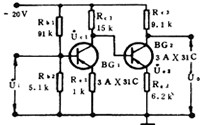
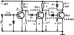
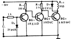
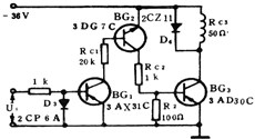
Single-ended DC amplifier circuit diagrams
Single-ended DC amplifiers need to solve the problem of inter-stage DC level shifting. Using resistor Re2 to pull down the emitter potential of BG2 meets the DC level configuration requirements (i.e., Vbe2 = Vc1 - Ve2). Diodes D1 and D2 can be used for level shifting, setting the bias voltage of BG2 and BG3 to Vbe2 = 0.6V and Vbe3 = 0.6V respectively for silicon transistors (note: the original values of 0.3V and 0.45V were incorrect for standard silicon transistors). D3 provides protection to prevent excessive reverse bias on the base of BG1. If the output voltage of the front stage differs significantly from the input voltage requirements of the rear stage, zener diodes can replace standard silicon diodes to provide precise voltage level shifting. The circuit in Figure C uses larger collector resistors Rc1 and Rc2 to increase the collector voltage to achieve proper DC level configuration between stages. The circuit in Figure D uses complementary polarity transistors - PNP types (BG1 and BG3) and NPN type (BG2) - for level configuration. The output current of BG1 serves as the input current of BG2, and the output current of BG2 serves as the input current of BG3, realizing effective inter-stage coupling. The primary disadvantage of all four circuits shown is significant zero drift, which limits their use in precision applications.
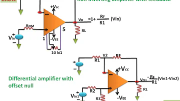
Ⅲ Differential DC Amplifier
A differential DC amplifier is composed of a pair of transistors BG1 and BG2 with matched characteristics, and the circuit components are also symmetrical. The input signals are Vi1 and Vi2; the single-ended output signals are Vc1 and Vc2 respectively; the differential output is the difference between Vc1 and Vc2, that is, Vo = Vc1 - Vc2. The differential circuit has the following important characteristics:
1. Superior Zero Drift Suppression
The differential circuit has matched transistor characteristics and symmetrical circuit components. When temperature rises, the collector currents of both transistors increase by the same amount, that is, ΔIc1 = ΔIc2, and the differential output is Vo = ΔIc1·Rc - ΔIc2·Rc = 0. Therefore, the output exhibits no zero drift. This is the primary advantage of differential amplifier topology and is why it forms the basis of virtually all modern precision amplifier designs.
2. Excellent Common-Mode Rejection
A pair of input signals with the same amplitude and the same phase is called a common-mode signal. When Vi1 = Vi2, under symmetrical conditions, the differential output Vo = K·Vi1 - K·Vi2 = 0. This means that noise, interference, and other unwanted signals that appear equally on both inputs are rejected, while only the difference signal is amplified. This is quantified by the Common-Mode Rejection Ratio (CMRR), typically expressed in decibels (dB).
3. Differential-Mode Signal Amplification
A pair of input signals with equal amplitude and opposite phase are called differential-mode signals. When Vi1 = -Vi2 (differential mode input), the collector outputs are Vc1 = -K·Vi1 and Vc2 = -K·Vi2. Therefore, the differential-mode gain Avd is: Avd = (Vc1 - Vc2)/(Vi1 - Vi2) = (-K·Vi1 - (-K·Vi2))/(Vi1 - Vi2) = -K = -(hfe·Rc)/(Rs + hie), where hfe is the transistor current gain, Rc is the collector resistance, Rs is the source resistance, and hie is the input impedance.
Since both the differential input voltage and differential output voltage of the differential circuit are doubled compared to a single-transistor common-emitter amplifier circuit, the differential-mode gain Avd is equivalent to that of a single-transistor common-emitter configuration.
To improve zero drift suppression capability, the common-mode gain should be minimized while the differential-mode gain should be maximized. Therefore, the Common-Mode Rejection Ratio (CMRR = Avd/Avc) is used as a critical performance indicator to evaluate differential amplifier circuits. Modern precision differential amplifiers can achieve CMRR values exceeding 100 dB (100,000:1 ratio).
4. Stable Operating Point
The emitter resistance Re provides strong negative feedback for common-mode signals and temperature drift. For example, when temperature rises and both Ic1 and Ic2 increase simultaneously, the following negative feedback process occurs: Ic1↑, Ic2↑ → Ie↑ → Ve↑ → Vbe1↓, Vbe2↓ → Ic1↓, Ic2↓. As a result, the actual changes in Ic1 and Ic2 are significantly reduced. Here, Re acts as a current source, thereby stabilizing the static operating point. Obviously, the larger Re is, the greater the constant current effect and the stronger the ability to suppress zero drift. An auxiliary negative power supply can be used to maintain the emitter at an appropriate potential relative to ground. It is important to note that Re does not provide negative feedback for differential-mode signals, so it does not reduce the differential-mode gain. In modern designs, Re is often replaced with an active current source (using transistors or FETs) to provide even better performance.
Ⅳ Low Noise Ultra-Wideband DC Amplifier
Low-noise wideband DC amplifiers are widely used in intermediate frequency and video amplifiers, as well as in modern high-speed data acquisition systems. This type of circuit is primarily used to amplify video signals, pulse signals, or radio frequency signals. The bandwidth of the amplified signal can range from DC to several megahertz or even hundreds of megahertz or gigahertz in modern implementations. These amplifiers are extensively used in signal processing applications, including oscilloscopes, spectrum analyzers, software-defined radio (SDR), and high-speed communication systems.
In recent years, the rapid development of Ultra-Wideband (UWB) technology in covert communication, radar systems, and target detection has further increased bandwidth requirements for UWB signals, which can span from 3.1 GHz to 10.6 GHz according to FCC regulations. Therefore, the signal preprocessing circuits required by receiver front-ends must be low-noise ultra-wideband amplifiers capable of handling these extremely wide bandwidths while maintaining low noise figures.
The performance of ultra-wideband DC amplifiers directly affects the accuracy of signal detection and processing. Low noise, low zero drift, wide bandwidth, and high linearity have always been the focus of this type of amplifier design, which has important engineering significance and practical value. Modern research has produced amplifiers that can achieve ultra-wideband amplification with noise figures below 2 dB while maintaining flat gain across the entire bandwidth. Contemporary designs often employ techniques such as inductive peaking, negative feedback, and cascode configurations to extend bandwidth while controlling noise and maintaining stability. Advanced semiconductor processes, including SiGe BiCMOS and GaN HEMT technologies, have enabled significant improvements in both bandwidth and noise performance compared to earlier implementations.
Ⅴ What is the Difference Between a DC Amplifier and an AC Amplifier?
DC amplification and AC amplification are fundamentally different in their coupling methods and applications. The distinction between DC amplifiers and AC amplifiers is significant:
DC Amplifiers: Do not use capacitors to block DC at the input and output stages. They employ direct coupling between stages.
Advantages:
Can amplify signals down to DC (0 Hz)
No low-frequency distortion caused by coupling capacitors
Faithful reproduction of slow-changing signals
Essential for applications requiring DC response (sensors, instrumentation)
Disadvantages:
Static operating point of each stage is interdependent with preceding and following stages
Circuit adjustment and design are more complex
Susceptible to zero drift and DC offset
Output must be zero when input signal is zero (no DC component allowed in output)
Requires careful component matching and temperature compensation
AC Amplifiers: Use coupling capacitors at input and output to block DC components.
Advantages:
Capacitors block DC, making the static operating point of each stage independent
Circuit design and adjustment are simpler
No zero drift problems
Each stage can be optimized independently
More economical for audio and RF applications
Disadvantages:
Limited frequency response - cannot amplify DC or very low frequencies
Input and output DC blocking capacitors limit the low-frequency bandwidth
Phase shift at low frequencies
Signal distortion increases with the number of cascaded stages
Coupling capacitors can be large and expensive for very low-frequency applications
The choice between DC and AC coupling depends on the application requirements. Modern amplifier designs often incorporate both techniques, using AC coupling where DC response is not needed and DC coupling (with careful drift compensation) where DC or very low-frequency response is essential.
Ⅵ Modern Applications and Developments
Since 2021, DC amplifier technology has continued to evolve with several significant developments:
Integrated Circuit Implementations
Modern DC amplifiers are predominantly implemented as integrated circuits (ICs), offering:
Precision instrumentation amplifiers with offset voltages below 10 μV
Auto-zero and chopper-stabilized amplifiers with drift below 0.01 μV/°C
High-speed DC amplifiers with bandwidths exceeding 1 GHz
Low-power designs for battery-operated and IoT applications
Programmable gain amplifiers (PGAs) with digital control interfaces
Key Application Areas
Contemporary DC amplifiers are essential in:
Medical Instrumentation: ECG, EEG, and biosensor signal conditioning
Industrial Automation: Sensor interfaces for temperature, pressure, and strain gauges
Test and Measurement: Precision voltmeters, data acquisition systems
Automotive: Battery management systems, sensor signal conditioning
Telecommunications: Transimpedance amplifiers for optical receivers
Aerospace: Flight control systems and sensor interfaces
Advanced Techniques
Modern DC amplifier designs incorporate:
Dynamic Element Matching (DEM): Reduces offset and drift by periodically swapping matched components
Correlated Double Sampling (CDS): Eliminates offset and low-frequency noise
Ping-pong auto-zeroing: Provides continuous operation while nulling offset
Digital calibration: Uses microcontrollers to compensate for drift and nonlinearity
CMOS technology: Enables low-power, high-integration designs
Ⅶ Key Performance Parameters
When selecting or designing a DC amplifier, the following parameters are critical:
Input Offset Voltage (Vos): The DC voltage that must be applied to the input to make the output zero. Modern precision amplifiers achieve Vos below 10 μV.
Input Offset Drift (dVos/dT): Change in offset voltage with temperature, typically specified in μV/°C. High-performance amplifiers achieve drift below 0.1 μV/°C.
Common-Mode Rejection Ratio (CMRR): Ability to reject signals common to both inputs. Expressed in dB, with values of 100-140 dB typical for precision amplifiers.
Bandwidth: Frequency range over which the amplifier maintains specified performance. Can range from DC to GHz in modern designs.
Noise: Specified as input-referred voltage noise density (nV/√Hz) and current noise density (pA/√Hz).
Input Impedance: Should be high (typically >1 GΩ for FET-input amplifiers) to minimize loading of the source.
Slew Rate: Maximum rate of change of output voltage, important for large-signal applications.
Power Supply Rejection Ratio (PSRR): Ability to reject power supply variations, typically 80-120 dB.
Article Update Information:
This article was originally published in 2021 and has been updated in November 2025 to reflect current technology and industry standards. Updates include:
Corrected transistor base-emitter voltage values (Vbe) to standard 0.6V for silicon devices
Updated bandwidth specifications to reflect modern ultra-wideband capabilities (up to GHz range)
Added information on contemporary IC implementations and advanced techniques
Expanded application examples to include IoT, automotive, and modern medical devices
Added sections on modern developments and key performance parameters
Updated noise figure specifications and CMRR values to reflect current state-of-the-art performance
Corrected terminology and improved technical accuracy throughout
Enhanced mobile responsiveness of HTML formatting
Last updated: November 7, 2025
 UTMEL
UTMEL
We are the professional distributor of electronic components, providing a large variety of products to save you a lot of time, effort, and cost with our efficient self-customized service. careful order preparation fast delivery service
1.How does a DC amplifier work?
A direct-coupled amplifier or DC amplifier is a type of amplifier in which the output of one stage of the amplifier is coupled to the input of the next stage in such a way as to permit signals with zero frequency, also referred to as direct current, to pass from input to output.
2.What is the DC gain of an amplifier?
DC gain is the amplification (multiplication) of DC input voltage (at an OPAMP) A = U(out) / U(in); all under DC conditions. AC gain is the same as with DC, but you need to know what (AC) frequency. OPAMP circuits (with feedback = closed loop) that have different gain at different frequencies are called "filters".
3.Can DC be amplified?
Yes, you can amplify a DC voltage. Many signals in applications such as temperature, pressure, weighing, etc., change so slowly that they can be considered DC. The amplifiers that condition these signals will often use op-amps1 to buffer and boost the signal level.
4.What is the main advantage of a DC amplifier?
The advantages of the direct-coupled amplifier are as follows. The circuit arrangement is simple because of minimum use of resistors. The circuit is of low cost because of the absence of expensive coupling devices.
5.What is the major drawback of a DC amplifier?
Disadvantages of DC Amplifiers: The output can be changed by the time or the age & modify in supply voltage. The transistor parameters β & vbe can change by temperature. This can cause the change within CC (collector current) & voltage. Thus, the o/p voltage can be changed.
 Introduction to MD8002A Audio AmplifierUTMEL27 March 20259326
The MD8002A is an audio power amplifier that uses a 5V DC power supply to provide 2.0 watts of continuous power to a BTL load with less than 10% distortion. It was created with the aim of providing high-quality o/p control with fewer components. It doesn't use any output coupling capacitors or bootstrap capacitors.
Read More") Understanding the Low Noise Amplifier (LNA)UTMEL20 March 202525842
Understanding the Low Noise Amplifier (LNA)UTMEL20 March 202525842A low noise amplifier is an amplifier with a very low noise figure. It is generally used as a high-frequency or intermediate-frequency preamplifier for various types of radio receivers, as well as amplifying circuits for high-sensitivity electronic detection equipment.
Read More Introduction to Optical AmplifierUTMEL27 March 202510034
An optical amplifier is a subsystem product that can amplify optical signals in optical fiber communication systems. The principle of the optical amplifier is basically based on the stimulated radiation of the laser, which realizes the amplification effect by converting the energy of the pump light into the energy of the signal light.
Read More What is an Inverting Amplifier?UTMEL25 April 202511857
An inverting amplifier is a fundamental configuration of operational amplifiers where the output signal has opposite polarity to the input signal. This configuration uses an operational amplifier with its inverting input terminal receiving the input signal, while the non-inverting terminal is typically connected to ground. The primary function of this circuit is to amplify the input signal while inverting its phase by 180 degrees.
Read More Low-Power Design of Operational AmplifiersUTMEL27 March 20257314
Hello, this is Candy. With the rise in popularity of battery-powered electronics in recent years, analog circuit designers have been increasingly concerned about power usage. This article will cover how to use low-power op amps in system design, as well as low-power op amps with low supply voltage capabilities and their applications, as well as how to read and understand op amp data sheets appropriately. Circuit design with energy-saving technologies for more efficient device choices.
Read More
Subscribe to Utmel !
![LT4363MPMS-2#TRPBF]() LT4363MPMS-2#TRPBF
LT4363MPMS-2#TRPBFLinear Technology/Analog Devices
![MSMCJ17CAE3/TR]() MSMCJ17CAE3/TR
MSMCJ17CAE3/TRMicrochip Technology
![LTC4364CDE-2#PBF]() LTC4364CDE-2#PBF
LTC4364CDE-2#PBFLinear Technology/Analog Devices
![JANTX1N6037A/TR]() JANTX1N6037A/TR
JANTX1N6037A/TRMicrochip Technology
![LTC4368HMS-1#PBF]() LTC4368HMS-1#PBF
LTC4368HMS-1#PBFLinear Technology/Analog Devices
![TBU-CA025-050-WH]() TBU-CA025-050-WH
TBU-CA025-050-WHBourns Inc.
![01550900M]() 01550900M
01550900MLittelfuse Inc.
![SN65240PWRG4]() SN65240PWRG4
SN65240PWRG4Texas Instruments
![LT4363MPS-1#PBF]() LT4363MPS-1#PBF
LT4363MPS-1#PBFLinear Technology/Analog Devices
![M15KP30CA/TR]() M15KP30CA/TR
M15KP30CA/TRMicrochip Technology