Detecting Wafer Patterns using Semi-Supervised Learning
| Topics covered in this article: |
| Ⅰ. Motivation |
| Ⅱ. Phases in which the experiment was carried out |
| Ⅲ. Results obtained after Simulation |
| Ⅳ. Conclusion |
Despite living in the modern 21st century, where manufacturing systems have begun to become more automated, the fabrication process of various electronic parts such as the Integrated Circuit (IC) may result in errors. While conducting research in any field, it is important to study patterns of any kind to collect, analyze and interpret results.
When it comes to wafer tests of any form, results are achieved using wafer maps, which provide the location of the failed dies on the wafer.
Wafer defect patterns have been proved to identify errors during several tests using advanced statistical analysis. Initially, older methods were used wherein the data obtained turned out to be inaccurate leading to more problems in conducting experiments. Therefore, various new detection methods have come up to get more precise and accurate results in diverse fields.
Ⅰ. Motivation
The quality of the training dataset and the Machine Learning (ML) technique was applied to have an impact on a prediction model's performance. Regardless of the ML algorithm, an inconsistent training set will negatively impact the prediction model's performance.
A collection of labeled wafer maps could be seen to have different levels of labeling mistakes. For the WM-811K database, for instance, nine defect kinds have been identified: Center, Donut, Edge-local, Edge ring, Local, Near-full, Random, Scratch, and None. With relatively acceptable recognition results, seven of the nine fault types with visually discernible patterns can be identified (higher than 80 percent). However, a more thorough examination of the database exposes a number of dubious designations, as illustrated in this section.
1. Inconsistent Labeling
Inconsistent labeling is illustrated in Fig. 1 with a few examples. Despite the fact that they appear to be very similar, Fig. 1(a) is labeled as the centre and Fig. 1(b) as a donut. Figures 1(c) and 1(d) both belong in the Scratch type category, however, Figure 1(c) is labeled as Donut. It is clear that Fig. 1(a) and Fig. 1(c) have incorrect labels, which makes supervised learning difficult.

Fig 1 Examples of inconsistent labeling in WM-811K (a) Center, (b) Donut, (c) Donut, (d) Scratch.
2. Multiple Patterns
Multiple fault patterns may be represented in a more intricate wafer map. These patterns may have only one type of fault or a variety of defect types. Examples of intricate wafer maps with mixed defect pattern types can be found in Fig. 2, while wafer maps with multiple defect patterns of the exact type can be discovered in Fig. 3.

Fig 2 Examples of mixed defect patterns in a single wafer map

Fig 3 Examples of multiple defect patterns of the same type
3. Special Rare Patterns

Fig 4 Examples of special patterns.
In certain cases, some special defect patterns may tend to occur which are not correctly recognized as a distinct pattern type. Most of the time, these wafer maps are classified under a vague but related fault category. For instance, Local, None, Scratch, and Local are the labels for the four wafer maps in Fig. 4. In reality, each of the four defect patterns in Fig.4 can be categorized as a distinct sort of defect pattern. Nearly half of the wafers in Fig. 4(a) are defective dies, hence this figure should be categorized as Half-full. Fig. 4(b) does not show any pattern, yet the defect density is between None (low density) and Random (high density). Parallel (or vertical) lines make up the flawed pattern in Fig 4(c), whereas in Figure 4(d).
4. Semi-Supervised Framework
In order to make sure supervised learning works, accurate labeling of the training data is very crucial. To solve problems of inaccurate data, semi-supervised learning is one of the ideal methods as prediction models are built using the initial manually labeled data. The remainder of the unlabeled data which is not used is then classified using the model. Additionally, they are also used to identify labeled samples that do not fit the model. This algorithm is then trained using the improved labeling in different iterations.
If these samples cannot be assigned to an existing defect type, they are processed by the unsupervised algorithm to produce new defect types. The following cycle of the supervised learning algorithm is then trained using the improved labeling. To get the final enhanced labeling and categorization, the entire process might be repeated multiple times.
Ⅱ. Phases in which the experiment was carried out
A total of three phases were used in which data was studied through the experiment. The initial two phases were extracted using machine learning algorithms after which labeled wafer maps were used to build a prediction model in the third phase.

Fig 5 Semi-supervised framework of wafer map pattern recognition with enhanced labeling.
1. Phase 1 - Preprocessing: All items in the WM-811K database may not be specified properly and around 1.84 % of the wafer maps will be removed. The next step is to discard random defects to obtain cleaner patterns containing two local defect patterns and some randomly distributed defect patterns.
2. Phase 2 - Feature Extraction: The machine learning algorithms will extract all the supervised and unsupervised features. For geometric features, cluster defects need to be located which can be done through connected-component analysis (CCA). The second will contain the statistic features where four classes will be employed.
3. Phase 3 - Classification Model Construction: In phase three, a low tolerance classification model must be formed as per the labeled data present. Here, all the non-categorized data will get screened.
4. Phase 4 - Classifying Unlabeled Data: In phase four, all the unlabelled data from phase three will be taken into consideration if the probability is greater than the threshold of the previous phase. If unclassified, it will classify as an “error wafer”.
5. Phase 5 - Unsupervised Learning: Here, similar wafer maps will get clustered which have not been labeled yet. This is done by a self-organized map (SOM) which is an artificial neural network (ANN) model.
6. Phase 6 - Enhanced Labeling: New SOM models need to be labeled manually as some groups are very similar to existing defect pattern types. Such existing defect pattern types will get clubbed into the already existing ones.
Ⅲ. Results obtained after Simulation
The training set of the labeled samples is where all the phases started in the first iteration. The total number of labeled samples increased as some unlabeled samples are grouped into a defect type after each iteration. After each fifth iteration, there was hardly any change in the quantity of labeled data.

Fig 6 Accuracy after each iteration
The accuracy achieved is shown in the above fig wherein the first iteration was provided for reference and the prediction model is constructed by using training data. On seeing the results, the first iteration showed very high accuracy (97%). But when closely observed, the actual accuracy was less than 80%. This was due to a large number of wafers with no detected patterns.
Ⅳ. Conclusion
To understand and study automatic wafer detection maps, the supervised model and its algorithm has proved to show positive results. The use of manual and machine learning models can both be used in different cases.
To improve and identify defect types, semi-supervised learning can be very helpful for a number of applications.
 Discovering New and Advanced Methodology for Determining the Dynamic Characterization of Wide Bandgap DevicesSaumitra Jagdale15 March 20242448
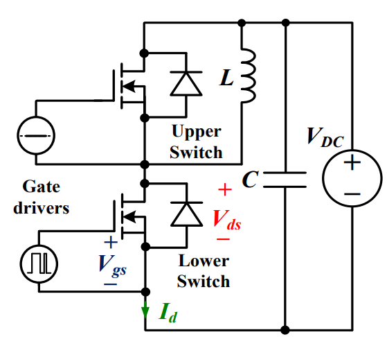
For a long era, silicon has stood out as the primary material for fabricating electronic devices due to its affordability, moderate efficiency, and performance capabilities. Despite its widespread use, silicon faces several limitations that render it unsuitable for applications involving high power and elevated temperatures. As technological advancements continue and the industry demands enhanced efficiency from devices, these limitations become increasingly vivid. In the quest for electronic devices that are more potent, efficient, and compact, wide bandgap materials are emerging as a dominant player. Their superiority over silicon in crucial aspects such as efficiency, higher junction temperatures, power density, thinner drift regions, and faster switching speeds positions them as the preferred materials for the future of power electronics.
Read More A Comprehensive Guide to FPGA Development BoardsUTMEL11 September 202513814
This comprehensive guide will take you on a journey through the fascinating world of FPGA development boards. We’ll explore what they are, how they differ from microcontrollers, and most importantly, how to choose the perfect board for your needs. Whether you’re a seasoned engineer or a curious hobbyist, prepare to unlock new possibilities in hardware design and accelerate your projects. We’ll cover everything from budget-friendly options to specialized boards for image processing, delve into popular learning paths, and even provide insights into essential software like Vivado. By the end of this article, you’ll have a clear roadmap to navigate the FPGA landscape and make informed decisions for your next groundbreaking endeavor.
Read More Applications of FPGAs in Artificial Intelligence: A Comprehensive GuideUTMEL29 August 20253424
This comprehensive guide explores FPGAs as powerful AI accelerators that offer distinct advantages over traditional GPUs and CPUs. FPGAs provide reconfigurable hardware that can be customized for specific AI workloads, delivering superior energy efficiency, ultra-low latency, and deterministic performance—particularly valuable for edge AI applications. While GPUs excel at parallel processing for training, FPGAs shine in inference tasks through their adaptability and power optimization. The document covers practical implementation challenges, including development complexity and resource constraints, while highlighting solutions like High-Level Synthesis tools and vendor-specific AI development suites from Intel and AMD/Xilinx. Real-world applications span telecommunications, healthcare, autonomous vehicles, and financial services, demonstrating FPGAs' versatility in mission-critical systems requiring real-time processing and minimal power consumption.
Read More 800G Optical Transceivers: The Guide for AI Data CentersUTMEL24 December 20253374
The complete guide to 800G Optical Transceiver standards (QSFP-DD vs. OSFP). Overcome supply shortages and scale your AI data center with Utmel Electronic.
Read More Xilinx FPGAs: From Getting Started to Advanced Application DevelopmentUTMEL09 September 20254161
This guide is your comprehensive roadmap to understanding and mastering the world of Xilinx FPGA technology. From selecting your first board to deploying advanced AI applications, we'll cover everything you need to know to unlock the potential of these remarkable devices. The global FPGA market is on a significant growth trajectory, expected to expand from USD 8.37 billion in 2025 to USD 17.53 billion by 2035. This surge is fueled by the relentless demand for high-performance, adaptable computing in everything from 5G networks and data centers to autonomous vehicles and the Internet of Things (IoT). This guide will walk you through the key concepts, tools, and products in the Xilinx ecosystem, ensuring you're well-equipped to be a part of this technological revolution.
Read More
Subscribe to Utmel !
![MOC3020VM]() MOC3020VM
MOC3020VMON Semiconductor
![HCS201T/SN]() HCS201T/SN
HCS201T/SNMicrochip Technology
![DLP6500BFYE]() DLP6500BFYE
DLP6500BFYETexas Instruments
![80HCPS1432CHMGI]() 80HCPS1432CHMGI
80HCPS1432CHMGIRenesas Electronics America Inc.
![MOC3082SVM]() MOC3082SVM
MOC3082SVMON Semiconductor
![DLP9500BFLN]() DLP9500BFLN
DLP9500BFLNTexas Instruments
![LTC3725EMSE#TRPBF]() LTC3725EMSE#TRPBF
LTC3725EMSE#TRPBFLinear Technology/Analog Devices
![MC68882RC50A]() MC68882RC50A
MC68882RC50ANXP USA Inc.
![LTC4213IDDB#TRMPBF]() LTC4213IDDB#TRMPBF
LTC4213IDDB#TRMPBFLinear Technology/Analog Devices
![FM31276-GTR]() FM31276-GTR
FM31276-GTRCypress Semiconductor Corp


 Product
 Brand
Brand Articles
 Tools
Tools


