
 Product
 Brand
Brand Articles
 Tools
Tools
What is a Decoder?
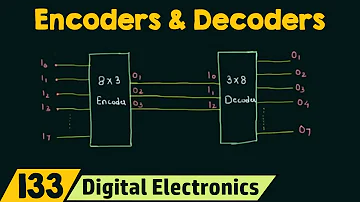
Introduction to Encoders and Decoders
2026 Executive Summary: A decoder is a fundamental combinational logic circuit in digital electronics that converts an n-bit binary input code into 2n unique output lines. Essential for memory address decoding, data routing, and 7-segment display control, decoders remain a core component in modern FPGA design and embedded systems education. This guide covers the 74LS138 (3-to-8 line) and CD4511 (BCD-to-7-segment) standards.
Catalog |
Ⅰ What is a decoder in digital electronics?
In digital electronics, a decoder is a combinational logic circuit that converts a binary input code (n lines) into a specific output line (2n lines). It acts as the reverse process of encoding, translating binary instructions into active signals for memory addressing, display control, or data routing. Ideally, for every unique input combination, exactly one output line is activated (set to High or Low depending on the logic).
Modern 2026 applications divide decoders into two primary categories:
Variable Decoding (Line Decoders): Converts minimal inputs into expanded outputs (e.g., n-to-2n line decoding like the 74LS138).
Display Decoding: Converts binary numbers into human-readable formats, such as 8421BCD to 7-segment display codes.
Ⅱ Classification & Key Types
While thousands of logic gates exist, decoders in 2026 are broadly classified by their input-output relationship and application. The design principles remain consistent across discrete ICs and modern FPGA implementations.
Binary Code Decoder (Min-term Decoder): This circuit activates one specific output line for each unique binary input combination. It is widely used in memory address selection.
Code Converter (Transcoding): Converts data from one format to another (e.g., BCD to Decimal, or Binary to Gray Code).
Display Decoder: Translates binary data into visual signals for devices like LED 7-segment displays or LCD screens.
Ⅲ Working Principle & Circuit Diagrams
A decoder functions as a "translator" logic circuit. It interprets the state of input binary codes and triggers a corresponding output signal. Most industry-standard decoders, such as the 74LS138, utilize Enable Inputs (Chip Select) to control whether the decoding function is active, a critical feature for expanding memory banks in computer architecture.

Figure 1. 74LS138 3-to-8 line decoder circuit
Analysis of the 74LS138 (Figure 1): This is a standard 3-to-8 line decoder. It features three input terminals (C, B, A) creating 8 possible binary states (000 to 111). These inputs decode into 8 specific output signals (Y0–Y7).
Enable Logic: The chip functions only when G1 is High (1) AND both G2A and G2B are Low (0).
Output Logic: It uses "Active Low" outputs, meaning the selected output line goes to logic 0 (Low), while all unselected lines remain at logic 1 (High).
Internal Circuit Structure
To understand how decoders operate at the silicon level, we look at the internal gate arrangement.

Figure 2. The internal structure of the decoder
2-to-4 Line Decoder Examples:
AND-Gate Implementation (Active High): In Figure 3, the outputs represent min-terms. For input 10 (Decimal 2), only output F2 goes High.
NAND-Gate Implementation (Active Low): In Figure 4, the outputs are inverted. For input 10, output F2 goes Low (0), while others stay High. This is the standard for most TTL chips like the 74LS138.
")
Figure 3. 2-input decoder composed of AND circuit (Active High)
")
Figure 4. 2-input decoder composed of NAND gate circuit (Active Low)
Realizing Logic Functions with Decoders
Decoders are versatile universal logic generators. Since a decoder generates all possible min-terms for a set of variables, any combinational logic function can be implemented by combining specific decoder outputs.
Example: implementing F(X,Y,Z) = ∑(0,1,4,6,7)
As shown in Figure 5, the implementation depends on the decoder's active state:
Fig 5a: Active High Output + OR Gate (Summing min-terms).
Fig 5d: Active Low Output + NAND Gate (Standard TTL method).

Figure 5. Realize logic function with decoder
The Role of Enable Inputs
Enable pins (E or G) allow multiple decoders to be cascaded (combined) to handle larger data widths. For example, two 2-to-4 decoders can be combined to create a 3-to-8 decoder using the Enable pin as the most significant bit (MSB).

Figure 6. Enable Inputs circuit
In Figure 7 below, the circuit demonstrates cascading. When input I2 is Low, the top decoder is enabled (Outputs 0-3). When I2 is High, the bottom decoder is enabled (Outputs 4-7). This principle is still used in 2026 for addressing RAM chips.

Figure 7. Use the enable terminal to convert two 2-input decoders into 3-input decoders
Standard Medium-Scale Decoder: The 74LS138
The 74LS138 remains the most cited example in digital logic education. Figure 8 details the pin assignments. Note the three enable pins: G1 (Active High), /G2, and /G3 (Active Low). This triple-enable configuration simplifies the process of connecting multiple chips without external inverters.

Figure 8. 3 to 8 decoder logic symbol, pin arrangement, and logic function
Display Decoding Technology
LED vs. LCD Display Drivers
Display decoders are specialized circuits that convert binary data (usually BCD) into the signals required to drive 7-segment displays.
LED Nixie Tubes (7-Segment LEDs): These use Light Emitting Diodes. They are robust and visible in the dark but require higher current. They come in Common Anode (requires active low driver) or Common Cathode (requires active high driver) configurations.
LCD Displays: Liquid Crystal Displays rely on ambient light (or backlights) and require very low power. Unlike LEDs, LCDs must be driven by an alternating pulse voltage (AC) to prevent damage to the liquid crystals.

Figure 9. The internal structure of the LED digital tube
LED Decoding: The CD4511
The CD4511 is the standard CMOS BCD-to-7-Segment latch/decoder/driver used for Common Cathode displays. Its outputs are Active High.

Figure 10. 4511's pin arrangement, logic symbols, and logic functions
Key CD4511 Pin Functions:
/LT (Lamp Test): When Low, all segments light up. Used to test for burned-out LEDs.
/BL (Blanking): When Low, all segments turn off. Used for pulse-width modulation (dimming) or suppressing leading zeros.
/ST (Store/Latch): Controls memory. When High, the display ignores changes at inputs A-D and holds the last valid number.
LCD Decoder Driver Differences
Driving an LCD is fundamentally different from an LED. LCD decoders do not output a simple High/Low voltage. Instead, they output a square wave (AC signal). If a DC voltage is applied to an LCD for an extended period, the liquid crystal material will degrade via electrolysis. Therefore, LCD drivers utilize phase differences between the backplane and segment frequencies to control visibility.
 UTMEL
UTMEL
We are the professional distributor of electronic components, providing a large variety of products to save you a lot of time, effort, and cost with our efficient self-customized service. careful order preparation fast delivery service
1. What is the purpose of decoders?
A decoder is a device that generates the original signal as output from the coded input signal and converts n lines of input into 2n lines of output. An AND gate can be used as the basic decoding element because it produces a high output only when all inputs are high.
2. How does decoder work?
A decoder is a combinational logic circuit that is used to change the code into a set of signals. A decoder circuit takes multiple inputs and gives multiple outputs. A decoder circuit takes binary data of 'n' inputs into '2^n' unique output. In addition to input pins, the decoder has a enable pin.
 Discovering New and Advanced Methodology for Determining the Dynamic Characterization of Wide Bandgap DevicesSaumitra Jagdale15 March 20242671
For a long era, silicon has stood out as the primary material for fabricating electronic devices due to its affordability, moderate efficiency, and performance capabilities. Despite its widespread use, silicon faces several limitations that render it unsuitable for applications involving high power and elevated temperatures. As technological advancements continue and the industry demands enhanced efficiency from devices, these limitations become increasingly vivid. In the quest for electronic devices that are more potent, efficient, and compact, wide bandgap materials are emerging as a dominant player. Their superiority over silicon in crucial aspects such as efficiency, higher junction temperatures, power density, thinner drift regions, and faster switching speeds positions them as the preferred materials for the future of power electronics.
Read More A Comprehensive Guide to FPGA Development BoardsUTMEL11 September 202520469
This comprehensive guide will take you on a journey through the fascinating world of FPGA development boards. We’ll explore what they are, how they differ from microcontrollers, and most importantly, how to choose the perfect board for your needs. Whether you’re a seasoned engineer or a curious hobbyist, prepare to unlock new possibilities in hardware design and accelerate your projects. We’ll cover everything from budget-friendly options to specialized boards for image processing, delve into popular learning paths, and even provide insights into essential software like Vivado. By the end of this article, you’ll have a clear roadmap to navigate the FPGA landscape and make informed decisions for your next groundbreaking endeavor.
Read More 800G Optical Transceivers: The Guide for AI Data CentersUTMEL24 December 202510791
The complete guide to 800G Optical Transceiver standards (QSFP-DD vs. OSFP). Overcome supply shortages and scale your AI data center with Utmel Electronic.
Read More The 2026 Engineer’s Guide: Choosing the Right MCU for Your Next IoT & New Energy ProjectUTMEL30 April 2026879
A comprehensive comparison of 2026's leading MCUs from ST, NXP, and Microchip across power efficiency, processing performance, connectivity, and ecosystems to help engineers select the optimal chip for next-gen IoT and new energy projects.
Read More AI Server Components: Engineering Next-Gen Data Center Hardware for 100kW RacksUTMEL15 May 2026426
The transition from traditional enterprise IT to AI-driven workloads has rendered legacy data center hardware obsolete, forcing infrastructure planners to re-engineer server components for extreme thermal environments.
Read More
Subscribe to Utmel !
![AD5520JSTZ]() AD5520JSTZ
AD5520JSTZAnalog Devices Inc.
![FOD3184SDV]() FOD3184SDV
FOD3184SDVON Semiconductor
![AT88SC0808CA-SH]() AT88SC0808CA-SH
AT88SC0808CA-SHMicrochip Technology
![AT88SC0204CA-SU]() AT88SC0204CA-SU
AT88SC0204CA-SUMicrochip Technology
![HCS200/SN]() HCS200/SN
HCS200/SNMicrochip Technology
![ACPL-332J-500E]() ACPL-332J-500E
ACPL-332J-500EBroadcom Limited
![FOD8320R2]() FOD8320R2
FOD8320R2ON Semiconductor
![ATECC108A-SSHCZ-B]() ATECC108A-SSHCZ-B
ATECC108A-SSHCZ-BMicrochip Technology
![HCS512-I/P]() HCS512-I/P
HCS512-I/PMicrochip Technology
![PAM8904JER]() PAM8904JER
PAM8904JERDiodes Incorporated


