What is an ASIC Chip?

ASIC: Application Specific Integrated Circuit
Executive Summary (2026 Update): ASIC chips (Application-Specific Integrated Circuits) have evolved from niche components to the backbone of the Artificial Intelligence and Internet of Things (IoT) revolution. Unlike general-purpose CPUs or GPUs, ASICs are custom-engineered for singular tasks, offering up to 70% higher energy efficiency for AI inference and specific algorithmic workloads. In 2026, the ASIC market is dominated by 2nm process nodes, chiplet architectures, and dedicated AI accelerators like Google's TPU v7 (Ironwood) and AWS Trainium. This guide explores the architecture, design process, and critical role of ASICs in modern computing.
Catalog |
Ⅰ What is an ASIC chip in 2026?
An ASIC (Application Specific Integrated Circuit) is a custom-engineered silicon chip designed to perform a singular, specialized task with maximum efficiency, rather than general-purpose processing. In the 2026 technology landscape, ASICs are the physical engines behind Generative AI (GenAI), cryptographic ledgers, and advanced automotive radar systems. Unlike general-purpose CPUs that handle diverse tasks sequentially, ASICs are hardwired to execute specific algorithms—such as the matrix multiplication in Neural Networks—at speeds and power efficiencies unattainable by other hardware.
At the hardware level, modern ASIC chips utilize cutting-edge manufacturing processes (ranging from mature 5nm nodes to state-of-the-art 2nm Gate-All-Around transistors). Physically, they are often constructed using Chiplet technology, where different modules (I/O, Compute, Memory) are stacked or linked via high-speed interconnects. These chips integrate vast arrays of IP cores, including High Bandwidth Memory (HBM3e), dedicated power management, and specialized security enclaves.
Key differentiators in 2026 include:
Extreme Efficiency: Tailored logic paths eliminate the "dark silicon" (unused transistors) found in general processors.
AI Dominance: The majority of Large Language Model (LLM) inference now runs on specialized ASICs (like TPUs and LPUs) rather than standard GPUs.
Miniaturization: System-on-Chip (SoC) designs integrate billions of transistors into footprints smaller than a fingernail for edge devices.
An integrated circuit is the fundamental building block of modern electronics. While early ICs invented by Jack Kilby and Robert Noyce in the 1970s contained a few dozen transistors, modern ASICs contain over 100 billion transistors. The shift towards ASICs is driven by the "End of Moore's Law" for general computing; to gain more speed, engineers must now customize the hardware to the software.
The larger the scale of integration, the more complex the system becomes. ASICs solve the bottleneck of general-purpose computing by embedding the entire system's logic—whether it is a 5G modem or a bitcoin miner—onto a single silicon die or package. This results in reduced latency, significantly lower power consumption (Joules per operation), and higher system reliability.
Ⅱ How are ASIC chips designed? (Process)
The ASIC design workflow in 2026 has evolved to include AI-driven Electronic Design Automation (EDA) tools, which automate complex placement and routing tasks. The core stages are:
Architectural Definition: The ASIC is divided into functional blocks (e.g., NPU cores, Memory Controllers). Engineers define the "PPA" targets: Performance, Power, and Area.
Logic Design (RTL): Engineers write the code that describes the chip's behavior using Hardware Description Languages (HDL) like Verilog or VHDL. This creates the Register Transfer Level (RTL) abstraction.
Verification & Emulation: Before manufacturing, the design is tested using Field-Programmable Gate Arrays (FPGA) or software emulation to ensure bug-free operation. In 2026, "Digital Twins" are often used to simulate thermal and electrical behaviors.
Physical Design (Place & Route): Logic synthesis tools map the RTL to a specific foundry process (e.g., TSMC 3nm). Billions of transistors are physically laid out on the virtual die.
Tape-out & Fabrication: The final blueprint (GDSII file) is sent to the foundry for manufacturing. This involves photolithography, etching, and packaging (often using advanced 2.5D CoWoS packaging).
Ⅲ Why choose ASICs over GPUs? (Pros & Cons)
While CPUs execute code sequentially and GPUs handle parallel graphics/math, ASICs are hardwired logic. This fundamental difference dictates their advantages and trade-offs in the 2026 market.
1. Key Advantages
Compared with CPUs, GPUs, and FPGAs, ASICs offer distinct benefits for high-volume, specific workloads:
① Area Efficiency: ASICs strip away the "bloat" of instruction decoders and branch predictors found in CPUs. A dedicated AI inference ASIC can be 5x smaller than a GPU with equivalent throughput.
② Energy Dominance: This is the primary driver in 2026. For large AI models, ASICs can consume 50-70% less power than GPUs. For example, while a data center GPU might consume 1000W, a specialized inference ASIC might deliver the same tokens/second at 300W.
③ Performance Density: Custom logic paths allow data to flow directly between execution units without writing back to memory as frequently, reducing latency.
④ Cost at Scale: While expensive to design, ASICs are cheap to reproduce. For consumer IoT devices, simple ASIC prices can be as low as $0.30 - $3.00, whereas general-purpose processors would cost significantly more.
2. Disadvantages
① High Upfront Cost (NRE): Designing a cutting-edge 3nm ASIC in 2026 can cost over $500 million in Non-Recurring Engineering fees. This makes them viable only for high-volume products.
② Lack of Flexibility: Once fabricated, the silicon cannot be changed. If the AI algorithm changes significantly (e.g., from Transformer to State Space Models), the ASIC may become obsolete, whereas a GPU can simply update its software drivers.
③ Time to Market: The development cycle is 12-24 months. By the time an ASIC is released, general-purpose GPUs may have already advanced in performance.
Ⅳ Classification of ASIC Architectures

ASIC chips Classification
(1) By Manufacturing/Design Methodology
The industry categorizes ASICs based on how much of the silicon is pre-defined vs. custom-drawn.
① Full-Custom ASIC Chips
In full-custom design, every single transistor and logic cell is hand-crafted for the application. This yields the highest possible performance and the smallest die area. It is reserved for high-volume, performance-critical applications like flagship smartphone processors or high-frequency trading chips.
② Semi-Custom ASIC Chips (Standard Cell)
This is the most common modern methodology. Designers use a library of pre-verified "Standard Cells" (logic gates, flip-flops) provided by the foundry. The design process focuses on arranging these cells rather than drawing individual transistors.
a. Gate Array (Legacy/Structured)
Gate arrays are wafers with pre-fabricated transistors. The customization happens only in the final metal interconnection layers. While less common in 2026 for high-end logic, "Structured ASICs" (like eASIC) act as a middle ground between FPGAs and Standard Cells.
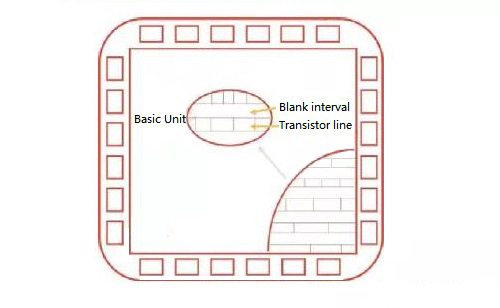
Channeled gate array ASIC chip
b. Standard Cell ASIC
Designers utilize vendor libraries for logical functions. In 2026, these libraries include complex "Macro" cells such as entire CPU cores (RISC-V or ARM), SRAM blocks, and high-speed SerDes interfaces.
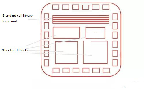
Standard Cell ASIC Chip
③ Programmable ASIC (PLD/FPGA)
While strictly distinct from ASICs, Programmable Logic Devices (PLDs) and FPGAs are often grouped here. They allow hardware logic to be reconfigured after manufacturing. They are often used for prototyping ASICs before mass production.
(2) By Application (AI Accelerators)
In the AI era, ASICs are often classified by the specific type of neural network processing they handle:
① TPU (Tensor Processing Unit): Developed by Google, these are specialized for the matrix math required by TensorFlow and JAX. The 2026 iterations (TPU v6/v7) focus heavily on "Inference at Scale."
② LPU (Language Processing Unit): A newer class of ASIC (e.g., from Groq) designed specifically to accelerate Large Language Models (LLMs) by optimizing memory bandwidth and sequential processing speed.
③ NPU (Neural Processing Unit): Commonly found in consumer electronics (smartphones, laptops) to handle background AI tasks like face recognition and voice isolation without draining the battery.
Ⅴ Top ASIC Examples in 2026
The ASIC market is currently defined by the "AI Arms Race" among hyperscalers. Key products include:
① Google TPU v7 (Ironwood) & Trillium: Google's latest custom silicon designed for the "Age of Inference." These chips feature massive High Bandwidth Memory (HBM) integration and optical interconnects to link thousands of chips into a supercomputer.
② AWS Trainium 3 & Inferentia: Amazon's custom silicon optimized for the EC2 cloud. Trainium 3 delivers industry-leading cost-to-train performance for massive generative models.
③ Microsoft Azure Maia 100: An AI accelerator chip designed specifically for Azure's cloud infrastructure to power workloads like OpenAI's ChatGPT.
④ Tesla Dojo (D1 Chip): A fully custom ASIC optimized for computer vision training to advance Full Self-Driving (FSD) capabilities.
⑤ Consumer Edge ASICs: Companies like Apple (A-series/M-series Neural Engine) and Qualcomm (Hexagon NPU) integrate powerful ASIC cores directly into consumer devices to enable on-device AI.
1.What are ASIC chips used for?
An ASIC, or application-specific integrated circuit, is a microchip designed for a special application, such as a kind of transmission protocol or a hand-held computer. You might contrast an ASIC with general integrated circuits, such as the microprocessor or random access memory chips in your PC.
2.What is ASIC chip technology?
An ASIC (application-specific integrated circuit) is a microchip designed for a special application, such as a particular kind of transmission protocol or a hand-held computer. You might contrast it with general integrated circuits, such as the microprocessor and the random access memory chips in your PC.
3.How does an ASIC chip work?
An ASIC miner refers to a device that uses microprocessors for the sole purpose of "mining" digital currency. Generally, each ASIC miner is constructed to mine a specific digital currency. So, a bitcoin ASIC miner can mine only bitcoin.
 Discovering New and Advanced Methodology for Determining the Dynamic Characterization of Wide Bandgap DevicesSaumitra Jagdale15 March 20242519
For a long era, silicon has stood out as the primary material for fabricating electronic devices due to its affordability, moderate efficiency, and performance capabilities. Despite its widespread use, silicon faces several limitations that render it unsuitable for applications involving high power and elevated temperatures. As technological advancements continue and the industry demands enhanced efficiency from devices, these limitations become increasingly vivid. In the quest for electronic devices that are more potent, efficient, and compact, wide bandgap materials are emerging as a dominant player. Their superiority over silicon in crucial aspects such as efficiency, higher junction temperatures, power density, thinner drift regions, and faster switching speeds positions them as the preferred materials for the future of power electronics.
Read More A Comprehensive Guide to FPGA Development BoardsUTMEL11 September 202516477
This comprehensive guide will take you on a journey through the fascinating world of FPGA development boards. We’ll explore what they are, how they differ from microcontrollers, and most importantly, how to choose the perfect board for your needs. Whether you’re a seasoned engineer or a curious hobbyist, prepare to unlock new possibilities in hardware design and accelerate your projects. We’ll cover everything from budget-friendly options to specialized boards for image processing, delve into popular learning paths, and even provide insights into essential software like Vivado. By the end of this article, you’ll have a clear roadmap to navigate the FPGA landscape and make informed decisions for your next groundbreaking endeavor.
Read More Applications of FPGAs in Artificial Intelligence: A Comprehensive GuideUTMEL29 August 20253993
This comprehensive guide explores FPGAs as powerful AI accelerators that offer distinct advantages over traditional GPUs and CPUs. FPGAs provide reconfigurable hardware that can be customized for specific AI workloads, delivering superior energy efficiency, ultra-low latency, and deterministic performance—particularly valuable for edge AI applications. While GPUs excel at parallel processing for training, FPGAs shine in inference tasks through their adaptability and power optimization. The document covers practical implementation challenges, including development complexity and resource constraints, while highlighting solutions like High-Level Synthesis tools and vendor-specific AI development suites from Intel and AMD/Xilinx. Real-world applications span telecommunications, healthcare, autonomous vehicles, and financial services, demonstrating FPGAs' versatility in mission-critical systems requiring real-time processing and minimal power consumption.
Read More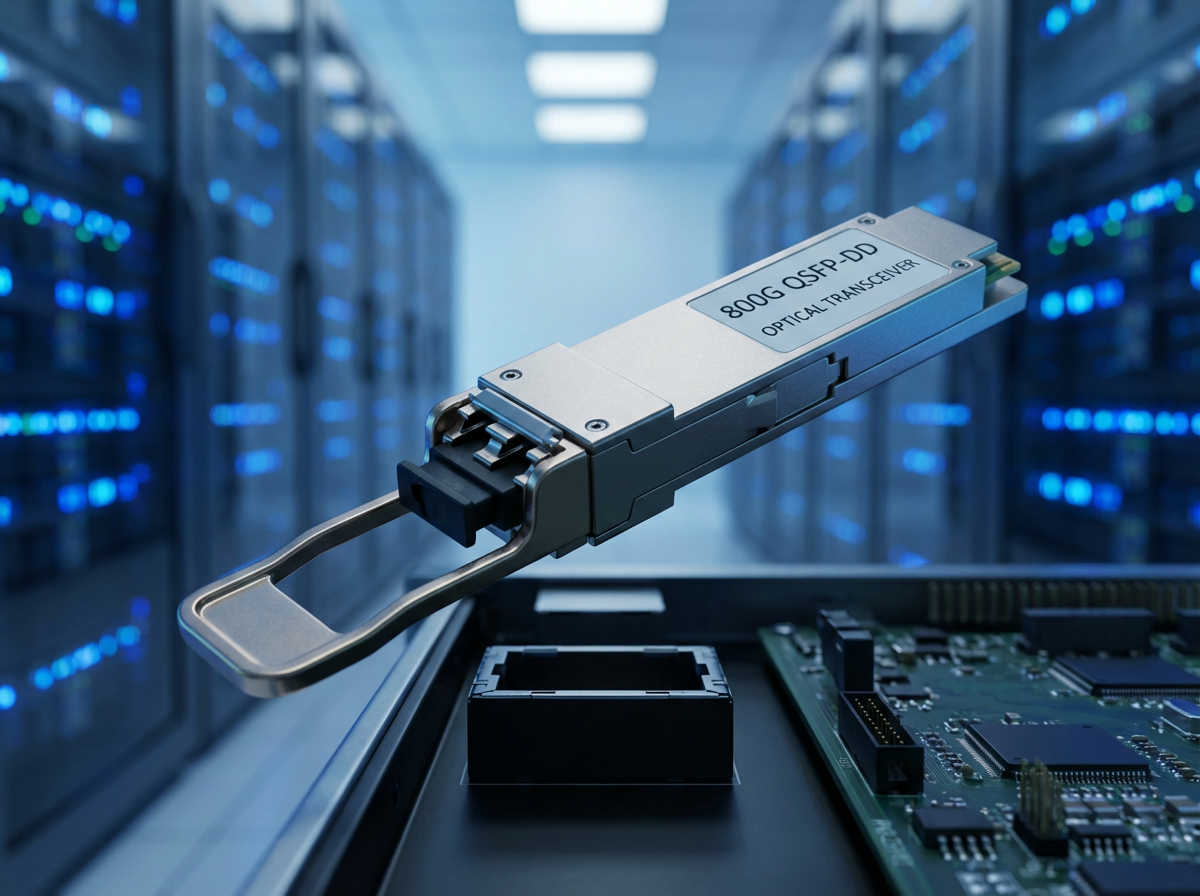 800G Optical Transceivers: The Guide for AI Data CentersUTMEL24 December 20255178
The complete guide to 800G Optical Transceiver standards (QSFP-DD vs. OSFP). Overcome supply shortages and scale your AI data center with Utmel Electronic.
Read More The 2026 Engineer’s Guide: Choosing the Right MCU for Your Next IoT & New Energy ProjectUTMEL30 April 2026196
A comprehensive comparison of 2026's leading MCUs from ST, NXP, and Microchip across power efficiency, processing performance, connectivity, and ecosystems to help engineers select the optimal chip for next-gen IoT and new energy projects.
Read More
Subscribe to Utmel !
![AD5520JSTZ]() AD5520JSTZ
AD5520JSTZAnalog Devices Inc.
![FOD3184SDV]() FOD3184SDV
FOD3184SDVON Semiconductor
![AT88SC0808CA-SH]() AT88SC0808CA-SH
AT88SC0808CA-SHMicrochip Technology
![AT88SC0204CA-SU]() AT88SC0204CA-SU
AT88SC0204CA-SUMicrochip Technology
![HCS200/SN]() HCS200/SN
HCS200/SNMicrochip Technology
![ACPL-332J-500E]() ACPL-332J-500E
ACPL-332J-500EBroadcom Limited
![FOD8320R2]() FOD8320R2
FOD8320R2ON Semiconductor
![ATECC108A-SSHCZ-B]() ATECC108A-SSHCZ-B
ATECC108A-SSHCZ-BMicrochip Technology
![HCS512-I/P]() HCS512-I/P
HCS512-I/PMicrochip Technology
![PAM8904JER]() PAM8904JER
PAM8904JERDiodes Incorporated


 Product
 Brand
Brand Articles
 Tools
Tools


