What is SPI (Serial Perripheral Interface)?

SPI: The serial peripheral interface
Ⅰ. Introduction to SPI Protocol
UART, I2C, and SPI are the three most used serial protocols for communication between separate chips aboard. The serial port protocol has previously been written. The SPI protocol will be introduced today. Motorola's Serial Peripheral Interface (SPI) is an acronym for Serial Peripheral Interface. A full-duplex, high-speed bus protocol.
SPI, like IIC, operates in a master-slave configuration. The slave is usually EPROM, Flash, AD/DA, audio and video processing chips, and other equipment, and the master is usually a programmable controller such as FPGA, MCU, or DSP. SCLK, CS, MOSI, and MISO are the four lines in general. SCK, SS, SDI, SDO, and other terms with similar meanings could be used. Select the Controlled slave device if there are several slaves. The key difference between normal SPI and TI's SSP protocol is the timing of chip select signals.

Ⅱ. 4-Wire or 3-2Wire?
By default, when we talk about SPI, we're talking about the normal 4-wire Motorola SPI protocol, which has four data lines: SCLK, MOSI, MISO, and CS. The typical 4-wire system has the advantage of being able to transmit data in full duplex mode. When only one master and one slave device are present, only one CS is required, however numerous slaves require several CSs. Each data line's introduction:
SCLK, the clock signal, the clock frequency is the SPI rate, and it is related to the SPI mode
MOSI, master output, slave input
MISO, master input, slave output
CS, slave device selection, active low
According to different application contexts, three-wire SPI is divided into two types:
There are only three wires: SCLK, CS, and DI or DO, which are ideal for simplex communication in which the host sends and receives data.

SCLK, SDIO, and CS are the only three wires. SDIO is used as a bidirectional port for half-duplex communication in this case. Many ADI ADC chips, for example, offer bidirectional communication. When employing an FPGA to operate a bidirectional port as an input, it should be set to a high-impedance state z.
Upgraded versions of the regular SPI protocol, such as Dual SPI, Quad SPI, and QPI, are also available. These protocols are beyond the purview of this section's explanation of the 3-wire/4-wire system, although they will be covered later in the article.
Ⅲ. 4 Working Modes
Because this is data transmission, both parties must specify when the slave will sample the data sent by the master and when the master will read the slave's data. It may not be as significant for STM32 and other MCU built-in hardware SPI peripherals. All you have to do now is set the mode. To implement SPI timing, however, it is critical to employ GPIO simulation or an FPGA. It has to do with the SPI standard protocol's functioning mode. It can be separated into four modes using different combinations of CPOL (Clock Polarity) clock polarity and CPHA (Clock Phase) clock phase.
In most cases, the slave device's working mode is set, and the master must follow suit in order for the two parties to communicate normally.
CPOL=0 means that SCK is 0 in idle state
CPOL=1 means that SCK is 1 in idle state
CPHA=0 means that the input and output data is valid at the first edge of SCK
CPHA=1 means that the input and output data is valid at the second edge of SCK
Modes 0 and 3 are the most commonly used of the four modes. Most SPI devices can work in both modes at the same time. These are, in reality, unimportant. In your device's handbook, you may find out which mode is used.
Take, for example, a Cypress ferroelectric memory FM25V05 that I recently employed in my work. Its official DataSheet states that it supports both SPI Mode 0 and Mode 3.

The read and write timing of SPI mode 0 can be determined using the timing diagram below. The SCK idle state is low in the figure, and the master data is sampled by the slave on each rising edge, with the data output being the same.

The SCK idle state is high in SPI mode 3, the slave samples the master data on each rising edge, and the data output is the same.

Modes 1 and 2 are identical. Mode 1 indicates that CPOL=0, CPHA=1, SCK idle is 0, and data is valid at the second edge of SCK, i.e. the falling edge of SCK.

Mode 2 indicates that CPOL=1, CPHA=0, SCK idle is 1, and data is valid at the first edge of SCK, i.e. the falling edge of SCK.

Setting the SPI mode of the host on some MCUs with built-in SPI hardware peripherals is relatively straightforward. You simply need to set the values of a few registers, as well as whether to write SCK high or low, and whether to use the first or second register. It is not necessary for the two edges to remember whether the value is 0 or 1. Consider the hardware SPI setup of the STM32F103:
SPI_InitTypeDef SPI_InitStruct;
SPI_InitStruct.SPI_Mode =SPI_Mode_Master; //host
.....
SPI_InitStruct.SPI_CPOL =SPI_CPOL_High; //SCK is high when idle
SPI_InitStruct.SPI_CPHA =SPI_CPHA_1Edge;//The first edge of SCK is valid
.....
SPI_Init(SPI2,&SPI_InitStruct);
But to realize in FPGA, need to control SCK and data input and output strictly according to timing.
Ⅳ. Multiple Transmission Rates
The rate of SCK is equal to the rate of SPI transmission. There is no set rate in the SPI protocol. The transmission rate of SPI, unlike IIC standard mode 100K, fast mode 400K, and high-speed mode 3.4M, is determined by how high the device supports, as specified in the device documentation. Take FM25V05, for example, which has a description:

Under various power supply voltages, the highest SCK clock frequency is:

Ⅴ. Basic Timing of SPI Protocol
When the CS value is low, the corresponding slave device is active. In each SCLK cycle, 1 bit data can be transferred. The sampling time is determined by the device's SPI mode. Formal data reading is done according to the control manner of various SPI devices. Before performing a write operation, the control word must be written first, followed by the register address and data. The write sequence for the FM25V05 ferroelectric memory in SPI mode 0 is shown below:

Read timing:

If you want to utilize FPGA to implement SPI timing, there must be a delay of at least 0.5 SCLK cycles between the falling edge of CS and the first edge of SCLK, or the rising edge of CS and the last edge of SCLK.

Some SPI slave devices support daisy chaining, which saves GPIO and reduces the amount of wiring required. However, daisy chain mode is not supported by all SPI devices.

Control Sequence:
Ⅵ. Upgraded Version of SPI Protocol
One SCLK cycle can only carry 1Bit data in the classic SPI protocol. Is it possible for a single SCLK to convey multiple bits of data? Yes, it is correct. Motorola has created a number of enhanced variants of the SPI protocol based on the existing standard 4-wire SPI protocol. The efficiency of data transmission can be enhanced by increasing the number of data lines. Many flash memory manufacturers already offer a variety of SPI protocols.
As an example, consider the W25Q128FW SPI Flash ROM. According to the device handbook, it supports Dual SPI, Quad SPI, QPI, and other modes in addition to the normal 4-wire SPI mode. IO0/1/ 2/3 of these IOs are used as bidirectional ports in these modes, resulting in a significant improvement in data read and write rates.

Read and write times for the QSPI protocol:

Models of Flash chips that implement the QSPI protocol include:

The SPI waveform was measured by the FPGA.
Serial timings such as UART, SPI, IIC, and others are implemented in FPGA. The state machine approach is the most often used implementation method, which separates down each step into individual states and then controls or reads the input based on the different states. The alignment of the data must be considered in the detail. Set-up and hold times, state jumps under unusual circumstances, and the inability to enter an infinite loop or become trapped in a particular state.
The waveform shown below uses a Xilinx FPGA to drive a ferroelectric memory FM25V05 with a typical 4-wire SPI protocol, which is identical to the ERPOM operation mode of the IIC interface: first, write the control word, then write the address, and then write or read the data. The frequency of the SCK clock is 40MHz. ChipScope's actually read and write waveforms can be used. At the low level of SCK, the data changes, but around the rising edge of SCK, the data should remain consistent.
It is critical to write the enable command first and then regenerate the CS signal in SPI write timing. This block has been stuck for a long time, and the issue is either in the official example's C code or in the manual's timing, which is not well understood.

Timing for the FM25V05 write
Write the control word first, then the 16-bit address, and then read the 8-bit data in the SPI read sequence.

FM25V05 read timing
Ⅶ. Comparison of SPI and IIC
SPI is full duplex, while IIC is half duplex.
IIC allows for several masters and slaves, but SPI only allows for one master.
IIC uses fewer GPIOs and saves resources from a GPIO occupancy standpoint.
SPI has a more flexible data width, and several data widths can be set as needed.
The SPI protocol lacks a response mechanism, therefore the host has no way of knowing whether the slave has received the data it transmitted. It is possible that data frames will be lost if certain procedures are not used.
The SPI protocol may achieve a very fast rate (up to hundreds of megabytes) and each SCK can transfer data precisely because there is no sophisticated response mechanism. Data can be sent at fast speeds by using CRC verification and other verification methods. It is capable of maintaining data accuracy.
The device address is used by IIC to pick the slave. While the SPI selects the slave through CS, an increase in the number of slaves will not result in an increase in GPIO. Each extra slave will require its own GPIO. It can, of course, be added by using a decoder. Make multi-slave control a reality.
The IIC is sampled on the SCL high-level device, whereas the SPI protocol is sampled on the edge of SCLK.
The majority of the two are utilized for on-board device communication over short distances.
Ⅷ. Summary
The most significant benefit of utilizing an FPGA to implement SPI timing is its versatility. The timing can be precisely modified to meet the needs of the user, and it can reach extremely high speeds. It has a lot of advantages to drive several chips at the same time. It's required in some cases of high-speed AD acquisition. The challenge with using FPGA to implement is that it is more difficult to do so, and it necessitates considerable debugging and simulation. Despite the fact that FPGA has some ready-to-use IP, it is still not versatile enough. Unlike MCUs like the STM32, which have ready-made library functions and registers, you may achieve master-slave mode, SPI mode, data bit width, various speeds, single-line dual-line, half-duplex full-duplex, DMA, and many other things with just a few lines of code. In summary, FPGA and MCU each have their own set of benefits and drawbacks. Choose according on your requirements! There is no agreement that cannot be reached, regardless of whatever controller is used for implementation. As long as the time is tightly controlled according to the data manual, nothing is impossible!
1. What is the difference between SPI and I/O?
I/O is the general term for input and output interfaces, and SPI specifically refers to a synchronous serial peripheral interface. SPI is a type of I/O.
2. What is the difference between IIC and SPI?
The IIC bus is a two-way, two-wire (SCL, SDA), serial, multi-master (mulTI-master) interface standard, with a bus arbitration mechanism, which is very suitable for short-distance, infrequent data communication between devices. In its protocol system, the device address of the destination device is always carried when transmitting data, so device networking can be realized. SPI occupies only four wires on the pins of the chip, which saves the pins of the chip, saves space and provides convenience for the layout of the PCB. It is precisely because of this simple and easy-to-use feature that more and more chips This communication protocol is integrated.
3. What does SIP stand for?
SIP stands for Serial Perripheral Interface.
 Discovering New and Advanced Methodology for Determining the Dynamic Characterization of Wide Bandgap DevicesSaumitra Jagdale15 March 20242455
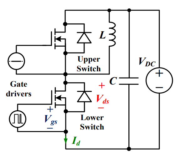
For a long era, silicon has stood out as the primary material for fabricating electronic devices due to its affordability, moderate efficiency, and performance capabilities. Despite its widespread use, silicon faces several limitations that render it unsuitable for applications involving high power and elevated temperatures. As technological advancements continue and the industry demands enhanced efficiency from devices, these limitations become increasingly vivid. In the quest for electronic devices that are more potent, efficient, and compact, wide bandgap materials are emerging as a dominant player. Their superiority over silicon in crucial aspects such as efficiency, higher junction temperatures, power density, thinner drift regions, and faster switching speeds positions them as the preferred materials for the future of power electronics.
Read More A Comprehensive Guide to FPGA Development BoardsUTMEL11 September 202514024
This comprehensive guide will take you on a journey through the fascinating world of FPGA development boards. We’ll explore what they are, how they differ from microcontrollers, and most importantly, how to choose the perfect board for your needs. Whether you’re a seasoned engineer or a curious hobbyist, prepare to unlock new possibilities in hardware design and accelerate your projects. We’ll cover everything from budget-friendly options to specialized boards for image processing, delve into popular learning paths, and even provide insights into essential software like Vivado. By the end of this article, you’ll have a clear roadmap to navigate the FPGA landscape and make informed decisions for your next groundbreaking endeavor.
Read More Applications of FPGAs in Artificial Intelligence: A Comprehensive GuideUTMEL29 August 20253475
This comprehensive guide explores FPGAs as powerful AI accelerators that offer distinct advantages over traditional GPUs and CPUs. FPGAs provide reconfigurable hardware that can be customized for specific AI workloads, delivering superior energy efficiency, ultra-low latency, and deterministic performance—particularly valuable for edge AI applications. While GPUs excel at parallel processing for training, FPGAs shine in inference tasks through their adaptability and power optimization. The document covers practical implementation challenges, including development complexity and resource constraints, while highlighting solutions like High-Level Synthesis tools and vendor-specific AI development suites from Intel and AMD/Xilinx. Real-world applications span telecommunications, healthcare, autonomous vehicles, and financial services, demonstrating FPGAs' versatility in mission-critical systems requiring real-time processing and minimal power consumption.
Read More 800G Optical Transceivers: The Guide for AI Data CentersUTMEL24 December 20253501
The complete guide to 800G Optical Transceiver standards (QSFP-DD vs. OSFP). Overcome supply shortages and scale your AI data center with Utmel Electronic.
Read More Xilinx FPGAs: From Getting Started to Advanced Application DevelopmentUTMEL09 September 20254195
This guide is your comprehensive roadmap to understanding and mastering the world of Xilinx FPGA technology. From selecting your first board to deploying advanced AI applications, we'll cover everything you need to know to unlock the potential of these remarkable devices. The global FPGA market is on a significant growth trajectory, expected to expand from USD 8.37 billion in 2025 to USD 17.53 billion by 2035. This surge is fueled by the relentless demand for high-performance, adaptable computing in everything from 5G networks and data centers to autonomous vehicles and the Internet of Things (IoT). This guide will walk you through the key concepts, tools, and products in the Xilinx ecosystem, ensuring you're well-equipped to be a part of this technological revolution.
Read More
Subscribe to Utmel !
![KSZ8993ML]() KSZ8993ML
KSZ8993MLMicrochip Technology
![AT88SC0404CA-SH-T]() AT88SC0404CA-SH-T
AT88SC0404CA-SH-TMicrochip Technology
![ATECC508A-MAHDA-T]() ATECC508A-MAHDA-T
ATECC508A-MAHDA-TMicrochip Technology
![ATECC608A-SSHDA-T]() ATECC608A-SSHDA-T
ATECC608A-SSHDA-TMicrochip Technology
![HCS500-I/SM]() HCS500-I/SM
HCS500-I/SMMicrochip Technology
![AT88SC0404CA-SH]() AT88SC0404CA-SH
AT88SC0404CA-SHMicrochip Technology
![FSSD06BQX]() FSSD06BQX
FSSD06BQXON Semiconductor
![AD5522JSVDZ]() AD5522JSVDZ
AD5522JSVDZAnalog Devices Inc.
![HCS515-I/SL]() HCS515-I/SL
HCS515-I/SLMicrochip Technology
![AT88SC0104CA-SH-T]() AT88SC0104CA-SH-T
AT88SC0104CA-SH-TMicrochip Technology


 Product
 Brand
Brand Articles
 Tools
Tools


