Product
 Brand
Brand Articles
 Tools
Tools
Design and Implementation of High Frequency Inverter for Printer Based on IR2110
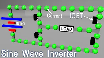
Sine wave inverter (SPWM) how its works?
| Topics covered in this article: |
| Ⅰ. System design scheme |
| Ⅱ. System hardware design |
| Ⅲ. System software design |
| Ⅳ. Conclusion |
Technologies such as switching power supplies have played an essential role in power electronics applications and diverse power supply systems in today's society. With the advancement of high-frequency switching power supply technology, it not only improves the appearance and structure of traditional circuits, but also considerably adds to the recycling efficiency of a portion of the power supply. saving materials and lowering costs. Inverter technology research is extremely important for the advancement of industrial technology and the enhancement of people's living conditions.
The inverter is a type of DC /AC (direct current/alternating current) conversion device that was used previously in the development of power electronics technology. The inverter is a device that converts direct current power into alternating current power while also providing control logic. Inverters are commonly utilized in electrical appliances in the home. The shape and installation of inverters are evolving in the direction of miniaturization, intelligence, and modularization in response to market development trends.
Ⅰ. System design scheme
The 220V power frequency voltage is initially input to the terminal of this paper's small inverter system, which then outputs the 24V AC voltage from the step-down transformer . The single-phase bridge rectifier circuit, two voltage regulator circuits, and several more circuits all contribute to the output 24V AC voltage. Two stable DC voltages (15 V and 5 V) are supplied after the diode is filtered to supply power to the microcontroller and the driver chip. At the same time, the PWM (pulse width modulation) wave generated after online serial programming the program into the microcontroller prompts two driver chips to generate two-phase four-channel PWM waves, which generate complementary high-pass and low-pass signals. A voltage-type full-bridge inverter circuit is constructed after driving the appropriate MOS (abbreviation for metal oxide semiconductor field effect transistor) tube. Finally, the load detects the generated complimentary rectangular wave; the output voltage is 220 V, 50 Hz AC voltage, the maximum output current is 2.5 A, and the maximum output power is not less than 100 W. The entire inverter process is finished as described above, and Figure 1 depicts the system design block diagram.

Figure. 1 System Design Scheme
Ⅱ. System hardware design
2.1 Driver chip IR2110
The American International Rectifier Company makes the IR2110 driver chip (now acquired by Infineon Corporation ). It has optocoupler isolation and electromagnetic isolation properties. It has become the driving device in most small and medium power conversion devices due to its tiny size and quick speed.
2.1.1 The working principle of IR2110
The internal functional structure of the driver chip IR2110 is made up of three primary parts: level shifting, logic input, and output protection. The various advantages of the IR2110 driver chip are the reason why the system circuit construction and design component can avoid many problems. In the design of a high-voltage floating bootstrap power supply circuit, for example, a group of power supplies effectively controls the higher and lower ports, reducing the number of extra driving power supplies to a minimum.
Figure 2 shows the drive half-bridge circuit of the IR2110 drive chip, which is a simple explanation of the bootstrap principle of the high-end side suspension drive circuit. C1 and VD1 are the bootstrap capacitor and bootstrap diode, respectively, and C2 is the filter capacitor for the supply voltage Vcc, as shown in the diagram.
To begin, it is expected that when S1 is turned off, the bootstrap capacitor C1 can endure a voltage of VC1 Vcc. VM1 is turned on, VM2 is turned off, and the VC1 voltage is applied between the gate of S1 and the source-emitter while HIN is in a high-level state. The bootstrap capacitor C1 then creates a loop through Rg1, VM1, gate, and source to discharge, causing VC1 to equal a voltage source and triggering S1 to switch on. The signals between HIN and LIN, on the other hand, are known to be complementary inputs. When LIN is low, VM3 is disabled and VM4 is enabled. The charge is quickly released to ground through Rg2 in S2's gate and the chip inside the source at this point. electricity is a type of energy. The dead time is affecting it at this time, causing S2 to be turned off before S1 is switched on.

Figure. 2 Internal Working Principle Diagram of IR2110
VM1 is turned off and VM2 is turned on when HIN is in the low level condition. At this point, the charge in S1's gate will be rapidly discharged through Rg1 and VM2, causing S1 to turn off. After a brief period of dead time (td), LIN rises to a high level, causing S2 to turn on and the power supply voltage Vcc to charge the bootstrap capacitor C1 via S2 and VD1, resulting in a quick increase of power to the bootstrap capacitor C1. Repeat this cycle.
2.1.2 IR2110 inverter circuit
Figure 3 is a schematic illustration of the IR2110 inverter. The IR2110 driver chips U3 and U4 are two of them. Four MOS transistors are used in Q1, Q2, Q3, and Q4. The PIC16F716 microcontroller outputs to the driver are Ua, Ub, Va, and Vb. The upper and lower arms of one-phase PWM wave are Ua and Ub, and Va and Vb are the upper and lower arms of another-phase PWM wave, as shown in the picture for the two-phase four-way PWM wave of the chip pin. The output to the driver chip is triggered by the PIC16F716 microcontroller. Because a portion of the PWM wave is incapable of driving high-power MOS tubes, the diodes D9 and D15 (using the Schottky tube's fast recovery function) must rely on the capacitor bootstrap function in IR2110 to increase capacitor charging. charge the bootstrap capacitors C11, C12, C16, C17, in order to increase the signal terminal voltage of the driving MOS tube, so that it has the function of boosting the output of the signal terminal, thus the increased signal terminal voltage The MOS transistors Q1, Q2, Q3, and Q4 can be turned on and off constantly using the PWM wave. Furthermore, the driving signals in the inverter circuit are complementary between the upper and lower arms of the same phase.

Figure. 3 IR2110 Inverter Schematic Diagram
Figure 3 shows that while Ua is in a high-level state, the output terminal HO1 is likewise in a high-level state, allowing the IR2110 chip's capacitor bootstrap function to regulate the MOS transistor Q1's opening. At the same time, the MOS transistor Q4 is in an off state since the output terminal LO1 is at a low level and cannot drive it. A high level is also input to Vb at the same time, indicating that the output terminal LO2 is in a high level condition, after which the MOS transistor Q3 is turned on and Q2 is turned off. As a result, a path is constructed via HO1 Q1 P2 Q3 GND. When Ua and Vb are in a low-level state and Ub and Va are in a high-level state, the current flow becomes a path from HO2 Q2 P2 Q4 GND, and the switching device (4 MOS transistors) is turned on and off alternately in an orderly manner, resulting in the formation of alternating current at the P2 (load end) position. Because short circuits generated by simultaneous conduction between the upper and lower arms of the chip are common in real applications, additional dead time is added to the software design process to prevent short circuits and protect the proper operation of the entire circuit.
2.2 MCU system
Microchip's PIC series microcontrollers have a number of advantages, including multiple integrated peripheral modules, steady performance, a simple hardware system architecture, and low power consumption. As a result, the PIC16F716 microcontroller is chosen as the main controller of the inverter in this study. These characteristics considerably reduce the cost of circuit construction because the PIC16F716 microcontroller does not require an additional A/D (analog/digital) conversion chip and contains four 8-bit A/D conversion channels. At the same time, the PIC16F716 microcontroller includes features such as a built-in power-on delay timer (DWRT), dual-threshold brown-out reset circuit, programmable code protection, power-on reset circuit (POR), watchdog timer (WDT), oscillator Start-up timer (OST), on-chip RC oscillator, In-Circuit Serial Programming (ICSP), and more. These functional qualities can lower the cost of circuit devices and the number of external devices on a single-chip microcomputer, resulting in a smaller overall system equipment size and a significant cost benefit in practical applications. In this system architecture, the PIC16F716 microcontroller uses a half-bridge output topology with enhanced PWM mode (that is, the microcontroller can supply four outputs from P1A to P1D). In most circumstances, the half-bridge output mode can be achieved with just two pins. The output is used to drive a push-pull load. Figure 4 shows the pin diagram of the peripheral circuit of the PIC16F716 microcontroller small system, in which the half-bridge arm is usually controlled by RB1 and RB2 (a programmable dead zone is usually used to achieve delay purpose in order to avoid the shoot-through phenomenon of high-power devices in the half-bridge output mode), the RB5 /P1B pin is the PWM wave output signal, and the RB3 /CCP1/P1A pin is the complementary PWM wave In addition, the IR2110 chip drives the output signal.

Figure. 4 PIC16F716 Peripheral Circuit Diagram
2.3 Protection circuit design
A protective circuit is included in the design of the inverter power supply in this study, as shown in Figure 5. When the inverter output current reaches 2.5 A, the overcurrent current ACK exceeds 4.5 V, and the SPWM chip detects that the ACK surpasses 2.5 V, the inverter protection is activated, and the LED P light flashes. Aside from that, the LED L light flashes. The LC circuit is selected by the output filter circuit, which has the following design parameters: L = 1 mH, C = 3 uF, and a cut-off frequency of 2.5 kHz.
Ⅲ. System software design
3.1 The realization principle of PWM wave
In this research, we show how the PIC16F716 microcontroller's enhanced capture/compare/PWM module (hence referred to as the ECCP module) can quickly realize two-way output complementary symmetrical PWM waves. As long as the values of the three sections of the register CCP1CON, the period register PR2, and the pulse width register CCPR1L in the working mode of the ECCP module are set correctly, the requisite PWM wave can be created. Full-bridge, half-bridge, and various working modes are available for this module. The signal polarity is set to be active at high level in this software design, which uses the half-bridge mode. Two pins are utilized as outputs to drive push-pull loads in half-bridge output mode: the RB3 pin sends the PWM output signal, and the RB5 pin outputs the complementary PWM pass-through output signal. Furthermore, in the case of the half-bridge output mode, the programmable dead-time delay can avoid the phenomena in the half-bridge circuit.

Figure. 5 Inverter Protection Circuit
3.2 Parameter calculation and configuration
Two parameters must be determined in order to generate a PWM wave: the period T of the PWM wave and the pulse width Twidth of the PWM wave. The PWM wave must have a frequency of 50 Hz and a duty cycle of 30%, according to the design requirements. Period T = 1/F = 1/50=20 ms; Pulse width Twidth = 20 ms X 30% = 6 ms; Then, according to the corresponding formula, the initial value of the period register PR2 and the initial value of the pulse width register CCPR1L can be computed.
The key program code is as follows:
// Set the working mode to PWM mode CCP1CON = 0B10001100;
// Dead time control set PWM1CON = 0X01;
// Set TMR2 working mode T2CON = 0X00;
// Set the symmetrical pulse period parameter PR2 = g_Period;
// Set the pulse width value CCPR1L = g_DutyWidth;
// disable T2 interrupt TMR2IE = 0;
// start T2 timer TMR2ON = 1;
3.3 Program experimental results
After uploading the software to the microcontroller, turn on the test and measure the output waveforms of RB3 and RB5 using the dual trace oscilloscope, as shown in Figure 6. The size and direction of the signal change frequently with time, as shown in the figure, which satisfies the inverter. The outcome fits the inverter circuit's requirements after the peculiarities of the standard AC signal are taken into account.

Figure. 6 Output Waveform
Ⅳ. Conclusion
By merging the theory of the inverter circuit with single-chip technology, the design of an independent inverter power supply based on SPWM technology is finally achieved in this article. Experiments demonstrate that the output function of the PWM module of the microcontroller control chip PIC16F716 can be realized by using software programming to realize the output of SPWM wave sequence.
The inverter circuit in this work is designed as a full-bridge circuit. The Microchip PIC16F716 chip is used to finish the design of the SPWM special chip in the full-bridge inverter process, which not only simplifies the system circuit but also improves circuit efficiency and realizes circuit high frequency and structure miniaturization. The physical diagram of the rectifier inverter is shown in Figure 7.

Figure. 7 Rectifier Inverter
 UTMEL
UTMEL
We are the professional distributor of electronic components, providing a large variety of products to save you a lot of time, effort, and cost with our efficient self-customized service. careful order preparation fast delivery service
1. In the inverter power supply, is it the PWM control wave generated by the inverter circuit or the PWM generated by the microcontroller itself?
The PWM is generated by the microcontroller itself, and the inverter circuit does not generate PWM, because the inverter circuit is only a function of voltage transformation.
2. How does an SPWM inverter work?
SPWM is based on PWM, and the desired output sinusoidal voltage waveform is imagined to be composed of a group of equal-width and unequal-width segments, and then a set of impulses are used to correspond to equal equal-amplitude and unequal-width (that is, pulse width modulation) pulses Substitute them in turn to get the desired sinusoidal voltage waveform at the filter output.
3. What is the principle and implementation of the inverter?
It first converts alternating current into direct current, and then switches the direct current with electronic components. It becomes alternating current. Generally, the inverter with larger power uses thyristor. And set up a device to adjust the frequency, so that the frequency can be adjusted within a certain range. .It is used to control the number of revolutions of the motor. The number of revolutions can be adjusted within a certain range. The frequency converter is widely used in the speed regulation of AC motors. The frequency conversion speed regulation technology is an important development direction of modern power transmission technology. With the development of technology, AC frequency conversion technology gradually matures from theory to practice.
 Analysis of Wide Bandgap Devices in Renewable Energy SystemsSaumitra Jagdale11 April 20235114
The article will describe the Analysis of Wide Bandgap Devices in Renewable Energy Systems.
Read More Role of Solar Energy in Wide-Band Gap Devices for Photovoltaic ApplicationsSaumitra Jagdale15 March 20244570
The enhancement of photovoltaic systems is closely linked to advancements in power semiconductor devices. Traditional Silicon-based power devices face challenges in meeting market demands for various applications such as EV, PV systems, and other high-power requirements. Presently, power device boasts enhanced efficiency, higher power density, increased blocking voltage, increased switching frequency, reduced cost, and improved reliability.
Read More Modeling, Modulation Analysis of Filter-Integrated Three-Switch Boost InverterRakesh Kumar, Ph.D.12 April 20234739
This article discusses the importance of inverters in energy conversion, the need for filters to eliminate harmonics that can cause system loss and circuit failure, two types of inverters, and an analysis of the three-switch boost inverter topology.
Read More An Analysis of Current-Source Inverters Using High-Frequency WBG SwitchesSaumitra Jagdale09 May 20234913
Hello everyone, welcome to the new post today.
Read More Three Phase Inverter - 180 Degree Conduction ModeRakesh Kumar, Ph.D.05 October 202320588
This technical article illustrates the working of the three phase power electronics inverter in the 180 degree conduction mode. The operation of the six thyristors and the associated waveforms are shown for easier understanding.
Read More
Subscribe to Utmel !