When Designing a Power Supply, How to Consider the Selection of Topology?

Introduction to Power Topologies
Ⅰ. Introduction
The input voltage and output/input ratio are significant considerations when choosing a topology. The comparatively usable voltage ranges for commonly used isolated topologies are shown in Figure 1. The output power, the number of output voltage channels, and the output voltage adjustment range all play a role in topology selection. In general, a variety of topologies can be applied to a given situation, and it is impossible to say that one topology is absolutely suitable for a given application because product design also includes the designer's experience with a particular topology, whether components are easy to obtain, cost requirements, technical personnel requirements, debugging equipment and personnel quality, manufacturing process equipment, batches, military or civilian products, and so on. To choose the optimal topology, you must first understand the strengths and limitations of each topology, as well as the topology's application areas. The new power supply design may be labeled a failure in the first place if topology is picked at random.
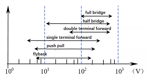
Figure. 1 Various Isolation Topologies Apply Voltage Ranges
Ⅱ. Input and output
A non-isolated Buck, Boost common ground converter can be utilized if the output and input are both in common ground. The structure of these circuits is simple, and there are just a few components. For safety reasons, the output should be isolated from the input if the input voltage is excessive.
You should first determine whether the output voltage is higher or lower than the input voltage within the input voltage variation range before selecting a topology. Buck converters, for example, can only be used when the output voltage is less than the input voltage, hence the output voltage should always be less than the input voltage. You can use Buck topology if you need to input 24V and output 15V; however, if the input 24V is between 8V and 80V, you can't use Buck converter since Buck converters can't convert 8V to 15V. A Boost topology must be employed if the output voltage is always higher than the input voltage.
There is a limit if the output voltage to input voltage ratio is too great (or too little). The voltage ratio is too large if the input voltage is 400V and the Buck converter is required to produce 48V. Despite the fact that the output voltage is always lower than the input voltage, this enormous voltage difference The switching frequency is limited by the voltage ratio, which does not exceed the control chip's minimum duty cycle range. Furthermore, the power device's peak current is considerable, and power device selection is challenging. If a topology with isolation is employed, the turns ratio can be used to alter the duty cycle. To improve the cost-effectiveness of the operation.
Ⅲ. Practical Limitations of Switching Frequency and Duty Cycle
1. Switching frequency
The switching frequency is the first consideration when building a converter. The major goal of increasing the frequency is to make the power supply smaller and lighter. The magnetic components of the power supply take up the most space and weight. Magnetic components in modern switching power supplies account for 20% to 30% of the volume (20% to 30%), weight (30% to 40%), and loss (20% to 30%) of the switching power supply.

According to the law of electromagnetic induction, U is the voltage applied by the transformer, N is the number of coil turns, A is the cross-sectional area of the magnetic core, B is the variation of the magnetic flux density, and f is the transformer's operating frequency.
The saturation of the magnetic material limits B at lower frequencies. As can be seen from the above calculation, when U is constant, the product of the number of turns and the cross-sectional area of the magnetic core is inversely proportional to the frequency in order to lower the volume of the magnetic core. The major way to lower the size of the power supply is to increase the frequency. Since the invention of switching power supply, this has been the primary research issue of innumerable scientific and technology researchers.
Is it possible to raise the switching power supply frequency indefinitely? Not at all. There are two major stumbling blocks: The loss of magnetic material is the first. Ferrite is commonly utilized at high frequencies, and its unit volume loss is calculated as follows:

f - working frequency; Bm - working magnetic induction amplitude The frequency and magnetic induction loss exponents are both greater than one. In general, =1.21.7; =22.7. The loss increases as the frequency rises. Lower the magnetic induction Bm at high frequency to reduce the loss so that it is not too significant, which defeats the aim of reducing volume. Otherwise, the loss is excessive, and efficiency suffers. Furthermore, the worse the heat dissipation conditions are, the larger the processing power of the magnetic core and the larger the volume, and the high-power magnetic core also restricts the switching frequency.
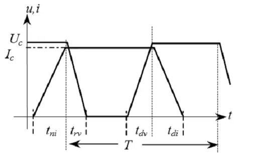
Figure. 2 Buck Converter Power Tube Current and Voltage Waveforms
Second, there is a switching loss limit for power devices. To demonstrate the switching loss, consider the Buck converter. Figure 2 shows a typical current-voltage waveform diagram of the current continuous Buck converter's power tube. The collector voltage does not begin to decline until the collector current reaches its maximum amount, as can be seen when the transistor is turned on. When the collector voltage is turned off, it initially increases to the maximum collector current before starting to decline. The increase and fall of voltage and current are considered to be linear. The switching loss can be calculated as follows:

When it is turned on, the sum of the current rising time and the voltage falling time is tr=tri trv; when it is turned off, the sum of the voltage rising time and the current falling time is td=tdi tdv. In most cases, tr tdT/20. Assume that the switching time is tr=td=ts. but:

Only the turn-off losses are present when the current is interrupted, and the switching losses are:

The switching loss is related to the frequency and switching duration, as can be observed. Although discontinuous switching loss appears to be half that of continuous switching loss, it should be noted that the current of the power tube is at least double that of the continuous current at the same output power. In addition to the device's increased current rating and cost, the conduction voltage drop loss increases as well. The forward transformer condition of the filter inductor core will considerably enhance the high frequency loss of the core and coil. Although soft switching approaches can reduce switching losses, keep in mind that soft switching always uses LC resonance, which has a significant resonance current (or voltage) that flows through the transistor, inductor L, and capacitor C, all of which are lossy components. The efficiency is sometimes only improved by 1-2 percent, but the circuit is complicated, the number of components increases, the cost increases, and the gain isn't always worth the loss.
MOSFET switching power supplies currently have a power rating of less than 5kW and a frequency of less than 200kHz. Up to 50kHz, BJT. Use the maximum 30kHz IGBT frequency over 3kW. The maximum frequency of a MOSFET and IGBT (BJT) combination tube is 100kHz. The conversion power is in the tens of watts, and the operating frequency is, of course, adjustable.
Furthermore, the higher the conversion power, the higher the current and voltage will be. If the current rises and falls at the same rate in both the high-power and low-power tubes, the high-power tube requires a longer switching time. Furthermore, because the chip area of high-power devices is big, the switching time is increased to avoid current concentration and lower the current rise and fall rate during switching. As can be observed, the higher the conversion power, the lower the switching frequency that can be used.
When you learn that his switching power supply's operational frequency can reach several MHz, you have to wonder how much conversion power he has.
2. Duty cycle
There is a limit to how large or small a switching converter's conversion ratio (output voltage to input voltage ratio) can be. The maximum and minimum settings of the control chip limit the converter duty cycle (ratio of switching on-time to switching period). The duty cycle in some topologies can't be higher than 0.5. In brief, most general-purpose PWM control IC chips do not guarantee a duty cycle more than 0.85; some chips do not promise a duty cycle lower than 0.05 at a suitable working frequency, and can fast drive the MOSFET gate with less loss.
If the switching frequency is 250 kHz and the period is 4 seconds, and the duty cycle is 0.1, the MOSFET's on-time is only 0.4 seconds; if the MOSFET's on-time is 0.1 seconds, the off-time is also 0.1 seconds, and practically all of the on-time is on. The changeover period "eats" time, and the loss rises. This is one of the reasons why the lower the operating frequency, the higher the conversion power.
Don't worry about the control IC and high current gate drive, as long as the duty cycle doesn't exceed the minimum 0.1 and maximum 0.8 (0.45 for a 0.5-limit converter).
The ratio can modify the duty cycle if the topology utilized incorporates a transformer. However, the ratio is constrained. The size of the main and secondary wires will be too varied if the transformation ratio is too large or too small, making coil winding difficult. The main to secondary turns ratio is typically 10:1 at the maximum and 1:10 at the minimum. Consider utilizing a two-stage converter or a voltage doubler circuit in the secondary to enhance the voltage if you require a high voltage from a very low voltage.
Ⅳ. How many outputs?
The topic of duty cycle immediately arises: how much should be output? Buck, for example, is unsuitable if there is more than one output. A follow-up regulator can be used to acquire a different voltage in some instances; a practical example would be a Buck converter to provide a 5V output and a linear regulator (or another switch) to get a 3.3V output from the 5V input. However, the associated transient, noise, and loss losses must match the standards.
In the worst-case scenario, instead of using complex magnetic elements with several coils, construct multiple independent converters. Before you start developing, keep in mind that while a multi-output converter may save you a few dollars on the control IC, that sophisticated multi-coil magnetic component could cost you dozens of dollars. The magnetic components, circuit components, and additional prices, not the facts, should be weighed first before designing.
Ⅴ. Isolation
Before designing, it is vital to know whether the secondary and primary need to be isolated. If the input is powered by a grid or high voltage, there are safety standards (and EMI concerns) that necessitate isolation as a commodity. A typical example is a 500V AC withstand voltage requirement for the input and output. Some topologies, such as Buck, Boost, and others, will be ruled out once the security needs are known.
Ⅵ. EMI
Consider EMI concerns from the start of the design process, rather than waiting until the end. Some topologies may have a lot of success in terms of avoiding EMI issues. Because there is no third wire in a non-isolated system, such as one that is only powered by batteries, there is no common-mode noise, making it easy to filter.
Aside from that, certain topologies are simply noisier than others. The distinction is that some topologies detach from the input for a portion of each cycle, causing the input current to be interrupted. The current will not be zero if the input current is continuous, there are no strong rising and falling edges, and it is easy to filter.
Because the input current is zero when the switch is open, a buck converter is an example of a discontinuous input current. The input loop is constantly connected to the inductance of the Boost converter, however, whether the input current is continuous depends on whether the Boost works sporadically or continuously.
I would advise against using topologies with discontinuous input current in high-power supplies, as these topologies frequently necessitate the employment of expensive magnetic components.
Ⅶ. BJT, MOSFET, or IGBT?
The power devices available influence topology selection. Bipolar (BJT) power transistors, MOSFETs, and IGBT s are the current power devices available. The bipolar tube's voltage rating can exceed 1.5kV, but it's more commonly used below 1kV, and the current ranges from several mA to hundreds of A; MOSFET's voltage rating is below 1kV, but it's more commonly used below 500V, and the current is several A to hundreds of A, and IGBT's voltage rating is above 500V, but it's more commonly used below 500V. The current is tens of A to several kA up to several kV.
Bipolar transistors are current-driven, while high-power high-voltage transistors have poor current gain and are frequently employed in single-switch topologies. Except for exceptional reasons, 90% of MOSFETs are used in the low to medium power range.
One factor is financial. If the product volume is high, bipolar is still less expensive than MOSFETs. The usage of bipolar power transistors, however, means that the switching frequency is lower than that of MOSFETs, resulting in relatively large magnetic components. Is it really worth it? You must carefully examine the research charges.
When the input voltage is large (380V), or the push-pull topology and transient voltage demand more than double the voltage, picking a power tube might be embarrassing. You can purchase a 1500V bipolar tube if you use one. MOSFETs can be purchased at a maximum voltage of 1000V, and their on-resistance is higher than that of BJTs. Of course, you could use IGBT s, however, these are driven similarly to MOSFETs, but switch at a faster rate than bipolar and have major smearing issues.
It can be seen that below low voltage (500V), the world of MOSFETs reigns supreme, with low power (hundreds of watts) switching frequencies in the hundreds of kHz range. IGBTs have a voltage rating of over 500V and a current rating of many tens of amps. It primarily serves as a speed regulator, replacing the high-voltage Darlington bipolar tube. The operating frequency can be up to 30kHz, usually around 20kHz. Because the on-voltage drop is large, it is not used below 100V.
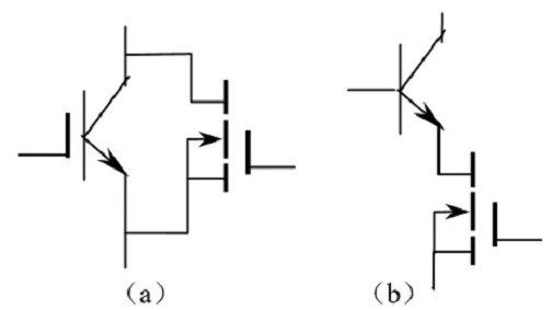
Figure. 3 Increasing Power Switching Frequency(a) IGBT in Parallel with MOSFET(b) BJT in Series with MOSFET
MOSFET can be used with BJT or IGBT to make a composite tube to improve the switching speed of IGBT or BJT. The U(BR)CBO/70A BJT is linked in series with a 50V/60A MOSFET in Figure 3(b), which is employed in a three-phase 380V rectifier inductance filter input (510V) double-terminal forward excitation 3kW communication power supply. The power MOSFET is driven initially when it is turned on. The BJT operates in a common base configuration at this moment, and the emitter input current, or because the MOSFET is turned on and the drain voltage drops, causes the BJT emitter junction to be forward biased, resulting in a base and collector current. The proportional driving circuit creates positive feedback, causing the BJT to become saturated and turn on. When the BJT is turned off, the MOSFET is turned off first, followed by the emitter junction, which is reverse biased. The common emitter's base frequency is times that of the common emitter. Turn-off speed has been improved. The low-voltage MOSFET's on-resistance is in the order of m, and the conduction loss is negligible. The actual operating frequency of the circuit is 50kHz.
The switching characteristics of MOSFET are also used in the parallel connection of MOSFET and IGBT, To do this, the MOSFET and IGBT drives should be constructed in such a way that when the PWM signal is switched on, it can drive the MOSFET on at the same time or first, before turning on the IGBT, At zero voltage, the IGBT is turned on. Turn off the IGBT first, and the IGBT is shut off at zero voltage; the MOSFET is turned off after a set delay. The MOSFET bears the switching losses; the high-voltage MOSFET has a bigger conduction voltage drop than the IGBT during the turn-on phase, and the IGBT carries the majority of the current, allowing the IGBT to bear the conduction loss. Practical use of this combination uses a 50kHz frequency and a 3kW half-bridge architecture.
Ⅷ. Continuous or intermittent
Continuous or discontinuous inductor (including flyback transformer) and current (ampere turns): The inductor current in a discontinuous mode converter is 0 at some points during the cycle. Continuous current (ampere turns) requires enough inductance to keep the minimum load current ILmin (including dummy loads) constant, and the inductor should have current flowing at all times. that is

T-switching period; D=Ton/T-duty ratio; Ton-transistor conduction time are some of them. We assume that the rectifier's forward voltage drop is minor in comparison to the output voltage. You must enter discontinuous mode if the minimum load current is 0.
The general power supply has no-load requirements in the real power supply design, and the inductance volume cannot be too large. At low load, it must be intermittent. In this instance, a dummy load is occasionally used, and when the load current surpasses a certain threshold, the fictitious load is disconnected. Otherwise, it may generate stability issues in closed-loop control, necessitating careful design of the feedback compensation network.
The exception is synchronous rectification. With synchronous rectification, converter applications are always in continuous mode and have no minimum inductance restrictions.
Ⅸ. Synchronous rectification
Today, converter efficiency is (nearly) more essential than the cost in many low output voltage applications. The more expensive but highly efficient converters are really cheap from the user's perspective. When a computer is inefficient in terms of power, real computing time is often minimal, and standby time is considerable, resulting in higher electricity costs.
Consider synchronous rectification if efficiency is a priority. That example, MOSFETs are used in the output rectifier. Many IC driver chips are now available that can effectively drive both FETs and synchronous rectifiers.
Another purpose to employ synchronous rectification is to convert discontinuous current converters to continuous current converters. Because current can flow in both directions even when there is no load, this is the case (since MOSFETs can conduct in both directions). Using synchronous rectification eliminates the need to worry about mode transitions (which can cause converter instability) and ensures that the minimum inductance requirement is met at all times.
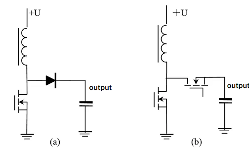
Figure. 4(a) Diode Rectifier Converter and (b) Synchronous Rectifier Converter
A problem worth mentioning is synchronous rectification. Before the synchronous rectification is turned on, the main switch is turned off, and vice versa. If this is disregarded, shoot-through will occur, in which the input (or output) voltage is shorted to ground, resulting in substantial losses and the possibility of failure. The inductor current continues to flow even when both MOSFETs are turned off. Because of its significant recovery period, the MOSFET body diode should not normally be used to flow current. When the MOSFET is turned off, it is presumed that the body diode continues to conduct current. In reverse recovery, when the body diode recovers, it behaves as a short circuit. As a result, punch-through occurs once the input (or output) is linked to the ground route, which might cause the converter to fail, as shown in Figure 4. (b) as seen.
A Schottky diode can be used in parallel with the MOSFET's body diode to alleviate this problem, allowing current to flow even when the MOSFET is switched off. (Because the Schottky's forward voltage drop is lower than the body diode's, the Schottky carries practically all of the current, and the body diode's reverse recovery time is proportional to the forward current before turning off, it may be neglected at this time.)
Ⅹ. Voltage type and current type control
A control difficulty in switching power supply design is determining whether to utilize voltage-type or current-type control. One of the two can be used in almost any topology. Current-mode control allows for cycle-by-cycle current limitation, making overcurrent protection simple to implement. Push-pull or full-bridge converters can overcome the output transformer's magnetic bias at the same time. However, if the current is really large, the current type will require a sensing resistor (which wastes a lot of power) or a transformer (which is expensive), which may influence your decision. The detection of overcurrent protection, on the other hand, is a piece of cake. When used in a half-bridge converter, however, the current-controlled kind may create voltage imbalance on the divider capacitor. So, if you need a lot of power, you need to think about which one is best.
Ⅺ. Conclusion
Before designing a power supply, it's vital to know what system your power supply will be used in. Learn more about the system's power requirements and limits. A detailed grasp of the system might help you save money and time during the design process.
In practice, you can construct a table out of the converter's specifications and go through them item by item. You'll notice that the number of topologies from which to pick is limited to one or two, and that topology selection is simply based on cost and size. A topology can be chosen in general depending on the factors listed above:
① Boost or Buck: Is the output voltage always higher or lower than the input voltage? If you don't, you won't be able to use Buck or Buck/Boost.
② Duty cycle: Is the output-to-input voltage ratio greater than 5? If this is the case, you will most likely require a transformer. Calculate the duty cycle to ensure it is neither excessively high or low.
③ How many output voltage settings are needed? A transformer is usually required if it is more than 1, unless a subsequent regulator is fitted. If there are too many output groups, numerous converters should be used.
④ Is it necessary to isolate yourself? What is the voltage? A transformer is required for isolation.
⑤ What are the EMI specifications? If the criteria are stringent, it is recommended that you employ the present continuous operating mode rather than a topology with discontinuous input current, such as Buck.
⑥ Is price a major consideration? BJT is a low-power, high-voltage transistor. IGBTs can be used if the input voltage is more than 500V. Instead, MOSFETs should be used.
⑦ Is it necessary to unload the power supply? Unless Question 8 is used, select Intermittent mode if necessary. You can also use dummy loads.
⑧ Is it possible to apply synchronous rectification? As a result, the converter current can remain constant independent of the load.
⑨ Is the output current significant? If this is the case, the voltage type should be utilized rather than the current type.
1. What is the circuit topology?
Circuit topology refers to the connection relationship of the circuit, or the connection relationship between the various electronic components that make up the circuit.
It is the composition structure. The switching power supply circuit has several typical structures, such as Buck, Boost, flyback, forward, half bridge, full bridge, etc. The actual circuit is also based on these structures and then specific.
2. How many types in circuit topologies?
Buck switching regulator topology, boost switching regulator topology, reverse polarity switching regulator topology, push-pull topology, forward converter topology, double-ended forward converter topology, interleaved forward converter topology, half-bridge converter topology , full bridge converter topology, flyback converter, current mode topology and current feeding topology, SCR resonant topology, CUK converter topology
3. What are the requirements of the switching power supply bridge topology and push-pull topology for the transformer core?
Most choose ferrite cores. The choice of magnetic core depends on your operating frequency. The size and B value are related to your switching frequency.
 LLC Converter with Planar Matrix Transformer for High-Current-High-Power ApplicationsSaumitra Jagdale15 March 20244731
The rise of data centres in recent years, driven by cloud computing and big data, has caused a significant increase in electricity consumption. In the United States alone, it exceeded 70 billion kWh by 2014, making up 1.8% of total national electricity usage.
Read More Enhancing Frequency Stability in Modern Distributed Power SystemsRakesh Kumar, Ph.D.21 September 20244252
The article discusses the importance of primary frequency regulation in maintaining grid stability. It also explores battery energy storage systems, virtual synchronous generators, and advanced control strategies to enhance frequency stability in power systems.
Read More The Impact of SMPS on LED Lighting and Diverse IndustriesUTMEL05 June 20252596
Switched-Mode Power Supplies (SMPS) enhance LED lighting and industries by improving energy efficiency, reliability, and sustainability across diverse applications.
Read More What is Uninterruptible Power Supply (UPS)?UTMEL08 April 20215255
UPS is an uninterruptible power supply containing the energy storage device. It is mainly used to give a part of a device with a higher power stability, providing uninterrupted power supplies.
Read More Switch-mode Power Supply BasicsUTMEL14 December 20207863
Switched-mode Power Supply (SMPS), also known as switching converter, is a high-frequency electric energy conversion device and a type of power supply. Its function is to convert a level of voltage into the voltage or current required by the user through different forms of architecture.
Read More
Subscribe to Utmel !
![JW2SN-DC6V]() JW2SN-DC6V
JW2SN-DC6VPanasonic Electric Works
![JS1A-12V-F]() JS1A-12V-F
JS1A-12V-FPanasonic Electric Works
![ALZ12B12]() ALZ12B12
ALZ12B12Panasonic Electric Works
![ST1-DC12V-F]() ST1-DC12V-F
ST1-DC12V-FPanasonic Electric Works
![S4EB-12V]() S4EB-12V
S4EB-12VPanasonic Electric Works
![JTN1AS-PA-F-DC24V]() JTN1AS-PA-F-DC24V
JTN1AS-PA-F-DC24VPanasonic Electric Works
![ALE1PB24]() ALE1PB24
ALE1PB24Panasonic Electric Works
![DSP1A-DC12V]() DSP1A-DC12V
DSP1A-DC12VPanasonic Electric Works
![JQ1P-12V-F]() JQ1P-12V-F
JQ1P-12V-FPanasonic Electric Works
![2961150]() 2961150
2961150Phoenix Contact


 Product
 Brand
Brand Articles
 Tools
Tools


