
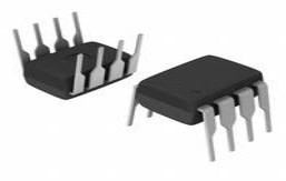
74LS08 AND Two Input Gate IC: Datasheet, Pinout and Voltage

74LS08N datasheet pdf and Unclassified product details from SIGNETICS CORP stock available at Utmel


74LS08 is a Quadruple 8-bit Two Input AND IC. This post mainly covers the datasheet, pinout, use, voltage, and other details about the 74LS08 gate IC. Furthermore, there is a huge range of semiconductors, capacitors, resistors, and ICs in stock. Welcome your RFQ!

Introduction to digital AND logic gate IC 74LS08
Overview of 74LS08
The 74LS08 AND Gate IC is part of the 74XXYY IC family. The chip contains four AND gates, each with two inputs, hence the name QUADRUPLE 2- INPUT AND GATE. The gates in the chip are designed by SCHOTTKY TRANSISTORS for high-speed logic operations.
74LS08 Pinout
The 74LS08 AND gate IC's pin diagram is given below. This IC has 14 pins, each of which is described below along with its function.

74LS08 Pinout
| Pin Number | Description |
| AND GATE 1 | |
| 1 | A1-INPUT1 of GATE 1 |
| 2 | B1-INPUT2 of GATE 1 |
| 3 | Y1-OUTPUT of GATE1 |
| AND GATE 2 | |
| 4 | A2-INPUT1 of GATE 2 |
| 5 | B2-INPUT2 of GATE 2 |
| 6 | Y2-OUTPUT of GATE2 |
| AND GATE 3 | |
| 9 | A3-INPUT1 of GATE 3 |
| 10 | B3-INPUT2 of GATE 3 |
| 8 | Y3-OUTPUT of GATE3 |
| AND GATE 4 | |
| 12 | A4-INPUT1 of GATE 4 |
| 13 | B4-INPUT2 of GATE 4 |
| 11 | Y4-OUTPUT of GATE4 |
| SHARED TERMINALS | |
| 7 | GND- connected to ground |
| 14 | VCC-Connected to a positive voltage to provide power to all four gates |
74LS08 CAD Model
Symbol

74LS08 Symbol
Footprint

74LS08 Footprint
Specifications
- TypeParameter
- Surface Mount
having leads that are designed to be soldered on the side of a circuit board that the body of the component is mounted on.
NO - Number of Terminals14
- Operating Temperature (Max.)70°C
- HTS Code
HTS (Harmonized Tariff Schedule) codes are product classification codes between 8-1 digits. The first six digits are an HS code, and the countries of import assign the subsequent digits to provide additional classification. U.S. HTS codes are 1 digits and are administered by the U.S. International Trade Commission.
8542.39.00.01 - Terminal Position
In electronic components, the term "Terminal Position" refers to the physical location of the connection points on the component where external electrical connections can be made. These connection points, known as terminals, are typically used to attach wires, leads, or other components to the main body of the electronic component. The terminal position is important for ensuring proper connectivity and functionality of the component within a circuit. It is often specified in technical datasheets or component specifications to help designers and engineers understand how to properly integrate the component into their circuit designs.
DUAL - Terminal Form
Occurring at or forming the end of a series, succession, or the like; closing; concluding.
THROUGH-HOLE - Number of Functions4
- Supply Voltage
Supply voltage refers to the electrical potential difference provided to an electronic component or circuit. It is crucial for the proper operation of devices, as it powers their functions and determines performance characteristics. The supply voltage must be within specified limits to ensure reliability and prevent damage to components. Different electronic devices have specific supply voltage requirements, which can vary widely depending on their design and intended application.
5V - JESD-30 Code
JESD-30 Code refers to a standardized descriptive designation system established by JEDEC for semiconductor-device packages. This system provides a systematic method for generating designators that convey essential information about the package's physical characteristics, such as size and shape, which aids in component identification and selection. By using JESD-30 codes, manufacturers and engineers can ensure consistency and clarity in the specification of semiconductor packages across various applications and industries.
R-PDIP-T14 - Qualification Status
An indicator of formal certification of qualifications.
Not Qualified - Supply Voltage-Max (Vsup)
The parameter "Supply Voltage-Max (Vsup)" in electronic components refers to the maximum voltage that can be safely applied to the component without causing damage. It is an important specification to consider when designing or using electronic circuits to ensure the component operates within its safe operating limits. Exceeding the maximum supply voltage can lead to overheating, component failure, or even permanent damage. It is crucial to adhere to the specified maximum supply voltage to ensure the reliable and safe operation of the electronic component.
5.25V - Temperature Grade
Temperature grades represent a tire's resistance to heat and its ability to dissipate heat when tested under controlled laboratory test conditions.
COMMERCIAL - Supply Voltage-Min (Vsup)
The parameter "Supply Voltage-Min (Vsup)" in electronic components refers to the minimum voltage level required for the component to operate within its specified performance range. This parameter indicates the lowest voltage that can be safely applied to the component without risking damage or malfunction. It is crucial to ensure that the supply voltage provided to the component meets or exceeds this minimum value to ensure proper functionality and reliability. Failure to adhere to the specified minimum supply voltage may result in erratic behavior, reduced performance, or even permanent damage to the component.
4.75V - Family
In electronic components, the parameter "Family" typically refers to a categorization or classification system used to group similar components together based on their characteristics, functions, or applications. This classification helps users easily identify and select components that meet their specific requirements. The "Family" parameter can include various subcategories such as resistors, capacitors, diodes, transistors, integrated circuits, and more. Understanding the "Family" of an electronic component can provide valuable information about its compatibility, performance specifications, and potential uses within a circuit or system. It is important to consider the "Family" parameter when designing or troubleshooting electronic circuits to ensure proper functionality and compatibility with other components.
LS - Number of Inputs2
- Logic IC Type
Logic IC Type refers to the type of integrated circuit (IC) that is specifically designed to perform logical operations. These ICs are commonly used in digital electronic devices to process and manipulate binary data according to predefined logic functions. The Logic IC Type parameter typically specifies the specific logic family or technology used in the IC, such as TTL (Transistor-Transistor Logic), CMOS (Complementary Metal-Oxide-Semiconductor), or ECL (Emitter-Coupled Logic). Understanding the Logic IC Type is important for selecting the appropriate IC for a given application, as different logic families have varying characteristics in terms of speed, power consumption, and noise immunity.
AND GATE - Propagation Delay (tpd)
Propagation delay (tpd) is a crucial parameter in electronic components, especially in digital circuits. It refers to the time taken for a signal to travel from the input of a component to its output. This delay is caused by various factors such as the internal circuitry, interconnections, and the physical properties of the component. Propagation delay is essential to consider in designing circuits to ensure proper timing and functionality. It is typically measured in nanoseconds or picoseconds and plays a significant role in determining the overall performance and speed of electronic systems.
20 ns
74LS08 Features
Low power consumption
Typical Rise Time: 18ns
Typical Fall Time: 18ns
Operating voltage range: +4.75 to +5.25V
Recommended operating voltage: +5V
Maximum supply voltage: 7V
Maximum current allowed drawing through each gate output: 8mA
TTL outputs
Operating temperature: 0°C to 70°C
Storage Temperature: -65°C to 150°C
74LS08 Applications
Digital Electronics
Networking Devices
Servers
Memory Units
ALU
General-purpose AND logic operation
Measuring Instruments
74LS08 Equivalents
74LS73, 74LS00, 74LS02, 74LS04, 74LS138, SN54LS08, IC 7408, HEF4081
Where to Use 74LS08 AND Gate
1. The chip is primarily employed when AND logic is required. The chip has four AND gates, and we can use one or all of them at the same time.
2. The chip is employed in systems that require both high speed and operation. As previously stated, SCHOTTKY TRANSISTORS built the gates on the chip to reduce gate switching delays. As a result, the chip can do high-speed AND operations.
3. The 74LS08 is one of the most affordable AND logic ICs on the market. It is extremely popular and widely available.
4. TTL outputs are provided by the chip, which is required in some systems.
How to Use 74LS08 AND Gate
To comprehend the 74LS08 AND gate IC, we must first comprehend the operation of a single AND logic gate. In general, an AND logic gate consists of three sorts of combinations, each of which has similar outputs on specific inputs.
Below is a diagram of a transistor-based logic AND gate circuit. Two transistors are utilized as switches in the following circuit to change the output condition for different inputs. Both transistors in the IC 74LS08 AND logic gate are linked in series. The power is applied to the collector terminal of the first transistor, and the output is obtained at the emitter terminal of the second transistor.

74LS08 Input Voltage
The two inputs are connected to the base terminal of both transistors. The inputs allow the current to travel between the two transistors. When the input signal is HIGH, current flows through the transistor, resulting in full voltages on the o/p pin.
In other cases, if one of the circuit's input pins is LOW, the o/p will also be LOW due to the current supply from the transistors. The output here will not be dependent on the type of AND gate, but will always be determined by the truth table of the AND gate, which is shown below.
A single AND gate or a combination of two AND gates cannot be used to create another logic gate, however, an AND logic gate can be used to create additional logic gates.
With just one NOT gate, an AND logic gate can be changed to a NAND logic gate. Other logic gates, such as XNOR and XOR, rely on AND logic gates; nevertheless, OR and NOT logic gates are required to create other logic gates.
74LS08 Dimensions


74LS08 Dimensions
74LS08 Manufacturer
Signetics is an American electronics manufacturer specifically established to make integrated circuits. Founded in 1961, they went on to develop several early microprocessors and support chips, as well as the widely used 555 timer chip. They were bought by Philips in 1975 and incorporated in Philips Semiconductors (now NXP).
What is 74LS08 used for?
74LS08 is a Quadruple 8-bit Two Input AND IC. Gate AND gate is a digital circuit used to convert the logic state to a specific logic. In AND gate two logics state signals are used. The first one is HIGH, which is also known as 3-5Volts and the second one is LOW which is represented by 0-2.6Volts.
How many gates are there in a regular 74LS08 chip?
There are four AND gates in the chip and each gate has two inputs, hence the name Quadruple 2- Input AND Gate. IC 74LS08 uses only one single power supply and it also comes in multiple packages to solve the requirement according to the circuit.
What is the difference between 7400 and 74LS00?
The 74LS00 family improves technically on the 7400 families in two key areas: faster speed and lower power consumption. The only limitation of the 74LS00 family compared to the 7400 families is that the 74LS00 family can only source half as much current.
What is the difference between 74LS08 and 74HC08?
74ls08 is a TTL circuit with a working power supply voltage of 5V. 74hc08 is a CMOS circuit, the chip power supply operating voltage range is 2V ~ 6V.
 TPS7A33: Regulator, Pinout, Circuit
30 March 20221455
 MCP6002 Op Amp: Circuits, Pinout, and Datasheet
20 December 202115664
 L7809CV Positive Voltage Regulator ICs: Pinout, Equivalent and Datasheet
28 February 20227010
 REF02 Voltage References: Circuit, Pinout, and Datasheet
06 July 20212637
 MSP430FG4619IPZ Mixed Signal Microcontroller: Comprehensive Technical Overview
29 February 202489
 1N4728A Zener Diode: Datasheet, Voltage and Specifications
30 September 20213989
 SG3525 Pulse width modulation controller IC: Datasheet, and Pinout
13 October 202219293
 1N914 Diode: Alternatives, Features and Datasheet
09 August 20217869
 An Overview of Common Mode Chokes
10 August 202013118
 Working Principle and Characteristics of Zener diodes
20 October 202523029
 What is 232\485\422 Communication? Common problems of Serial Communication
29 April 20221754
 FPGA Tutorial: A Beginner's Guide to Programmable Logic Design in 2025
15 April 20251709
 What are Motherboards?
23 June 20215692
 What is a Baseband Processor?
11 November 20217246
 Assessing the Effectiveness of Transient Voltage Suppressors in Modern Electronics
05 June 2025247
 Foreign Media Burst Samsung: DRAM, Foundry and Chip Defeat on All Fronts
20 April 20222282
SIGNETICS CORP
In Stock
United States
China
Canada
Japan
Russia
Germany
United Kingdom
Singapore
Italy
Hong Kong(China)
Taiwan(China)
France
Korea
Mexico
Netherlands
Malaysia
Austria
Spain
Switzerland
Poland
Thailand
Vietnam
India
United Arab Emirates
Afghanistan
Åland Islands
Albania
Algeria
American Samoa
Andorra
Angola
Anguilla
Antigua & Barbuda
Argentina
Armenia
Aruba
Australia
Azerbaijan
Bahamas
Bahrain
Bangladesh
Barbados
Belarus
Belgium
Belize
Benin
Bermuda
Bhutan
Bolivia
Bonaire, Sint Eustatius and Saba
Bosnia & Herzegovina
Botswana
Brazil
British Indian Ocean Territory
British Virgin Islands
Brunei
Bulgaria
Burkina Faso
Burundi
Cabo Verde
Cambodia
Cameroon
Cayman Islands
Central African Republic
Chad
Chile
Christmas Island
Cocos (Keeling) Islands
Colombia
Comoros
Congo
Congo (DRC)
Cook Islands
Costa Rica
Côte d’Ivoire
Croatia
Cuba
Curaçao
Cyprus
Czechia
Denmark
Djibouti
Dominica
Dominican Republic
Ecuador
Egypt
El Salvador
Equatorial Guinea
Eritrea
Estonia
Eswatini
Ethiopia
Falkland Islands
Faroe Islands
Fiji
Finland
French Guiana
French Polynesia
Gabon
Gambia
Georgia
Ghana
Gibraltar
Greece
Greenland
Grenada
Guadeloupe
Guam
Guatemala
Guernsey
Guinea
Guinea-Bissau
Guyana
Haiti
Honduras
Hungary
Iceland
Indonesia
Iran
Iraq
Ireland
Isle of Man
Israel
Jamaica
Jersey
Jordan
Kazakhstan
Kenya
Kiribati
Kosovo
Kuwait
Kyrgyzstan
Laos
Latvia
Lebanon
Lesotho
Liberia
Libya
Liechtenstein
Lithuania
Luxembourg
Macao(China)
Madagascar
Malawi
Maldives
Mali
Malta
Marshall Islands
Martinique
Mauritania
Mauritius
Mayotte
Micronesia
Moldova
Monaco
Mongolia
Montenegro
Montserrat
Morocco
Mozambique
Myanmar
Namibia
Nauru
Nepal
New Caledonia
New Zealand
Nicaragua
Niger
Nigeria
Niue
Norfolk Island
North Korea
North Macedonia
Northern Mariana Islands
Norway
Oman
Pakistan
Palau
Palestinian Authority
Panama
Papua New Guinea
Paraguay
Peru
Philippines
Pitcairn Islands
Portugal
Puerto Rico
Qatar
Réunion
Romania
Rwanda
Samoa
San Marino
São Tomé & Príncipe
Saudi Arabia
Senegal
Serbia
Seychelles
Sierra Leone
Sint Maarten
Slovakia
Slovenia
Solomon Islands
Somalia
South Africa
South Sudan
Sri Lanka
St Helena, Ascension, Tristan da Cunha
St. Barthélemy
St. Kitts & Nevis
St. Lucia
St. Martin
St. Pierre & Miquelon
St. Vincent & Grenadines
Sudan
Suriname
Svalbard & Jan Mayen
Sweden
Syria
Tajikistan
Tanzania
Timor-Leste
Togo
Tokelau
Tonga
Trinidad & Tobago
Tunisia
Turkey
Turkmenistan
Turks & Caicos Islands
Tuvalu
U.S. Outlying Islands
U.S. Virgin Islands
Uganda
Ukraine
Uruguay
Uzbekistan
Vanuatu
Vatican City
Venezuela
Wallis & Futuna
Yemen
Zambia
Zimbabwe