
 Product
 Brand
Brand Articles
 Tools
Tools
74LS73 Dual JK Flip-Flop IC: Datasheet, Pinout and How Do Flip Flops Work

74LS73N datasheet pdf and Unclassified product details from RAYTHEON SEMICONDUCTOR stock available at Utmel


The 74LS73 is a dual J-K Flip-flop with clear with LS technology and two independent J-K flip-flops with individual J-K, clock, and direct clear inputs. This article mainly explains datasheet, pinout, application, working, and other details about 74LS73 flip-flop.

JK Flip-flop Circuit & Working Explained
What is 74LS73?
The 74LS73 is a twin J-K flip-flop with clear and LS technology, as well as two independent J-K flip-flops having J-K, clock, and direct clear inputs. Two negative-edge-triggered flip-flops are included in the LS73A. For predictable functioning, the J and K inputs must be steady one setup time before the high-to-low clock change. When the clear is low, the clock and data inputs are overridden, causing the Q output to be low and the Q output to be high.
74LS73 Pin


74LS73 Pin
| Pin No | Pin Name | Description |
| 1 | CLK1 | Clock input pin 1 |
| 2 | CLR1― | Active low clear pin 1 |
| 3 | K1 | Input pin K1 |
| 4 | VCC | Supply Voltage |
| 5 | CLK2 | Clock input pin 2 |
| 6 | CLR2― | Active low clear pin 2 |
| 7 | J2 | Input pin J2 |
| 8 | Q2― | Active low output 2 pin |
| 9 | Q2 | Active high output 2 pin |
| 10 | K2 | Input pin K2 |
| 11 | GND | Ground Pin |
| 12 | Q1 | Active high output 1 pin |
| 13 | Q1― | Active low output 1 pin |
| 14 | J1 | Input pin J1 |
74LS73 Connection Diagram

74LS73 Connection Diagram
Specifications
- TypeParameter
- Surface Mount
having leads that are designed to be soldered on the side of a circuit board that the body of the component is mounted on.
NO - Number of Terminals14
- Operating Temperature (Max.)70°C
- JESD-609 Code
The "JESD-609 Code" in electronic components refers to a standardized marking code that indicates the lead-free solder composition and finish of electronic components for compliance with environmental regulations.
e0 - Terminal Finish
Terminal Finish refers to the surface treatment applied to the terminals or leads of electronic components to enhance their performance and longevity. It can improve solderability, corrosion resistance, and overall reliability of the connection in electronic assemblies. Common finishes include nickel, gold, and tin, each possessing distinct properties suitable for various applications. The choice of terminal finish can significantly impact the durability and effectiveness of electronic devices.
Tin/Lead (Sn/Pb) - Terminal Position
In electronic components, the term "Terminal Position" refers to the physical location of the connection points on the component where external electrical connections can be made. These connection points, known as terminals, are typically used to attach wires, leads, or other components to the main body of the electronic component. The terminal position is important for ensuring proper connectivity and functionality of the component within a circuit. It is often specified in technical datasheets or component specifications to help designers and engineers understand how to properly integrate the component into their circuit designs.
DUAL - Terminal Form
Occurring at or forming the end of a series, succession, or the like; closing; concluding.
THROUGH-HOLE - Number of Functions2
- Supply Voltage
Supply voltage refers to the electrical potential difference provided to an electronic component or circuit. It is crucial for the proper operation of devices, as it powers their functions and determines performance characteristics. The supply voltage must be within specified limits to ensure reliability and prevent damage to components. Different electronic devices have specific supply voltage requirements, which can vary widely depending on their design and intended application.
5V - Terminal Pitch
The center distance from one pole to the next.
2.54mm - JESD-30 Code
JESD-30 Code refers to a standardized descriptive designation system established by JEDEC for semiconductor-device packages. This system provides a systematic method for generating designators that convey essential information about the package's physical characteristics, such as size and shape, which aids in component identification and selection. By using JESD-30 codes, manufacturers and engineers can ensure consistency and clarity in the specification of semiconductor packages across various applications and industries.
R-PDIP-T14 - Qualification Status
An indicator of formal certification of qualifications.
Not Qualified - Power Supplies
an electronic circuit that converts the voltage of an alternating current (AC) into a direct current (DC) voltage.?
5V - Temperature Grade
Temperature grades represent a tire's resistance to heat and its ability to dissipate heat when tested under controlled laboratory test conditions.
COMMERCIAL - Logic IC Type
Logic IC Type refers to the type of integrated circuit (IC) that is specifically designed to perform logical operations. These ICs are commonly used in digital electronic devices to process and manipulate binary data according to predefined logic functions. The Logic IC Type parameter typically specifies the specific logic family or technology used in the IC, such as TTL (Transistor-Transistor Logic), CMOS (Complementary Metal-Oxide-Semiconductor), or ECL (Emitter-Coupled Logic). Understanding the Logic IC Type is important for selecting the appropriate IC for a given application, as different logic families have varying characteristics in terms of speed, power consumption, and noise immunity.
J-K FLIP-FLOP - Trigger Type
Trigger Type in electronic components refers to the mechanism or method by which a device, such as a flip-flop or timer, responds to an input signal. It defines how the device transitions between states based on specific conditions, such as rising or falling edges of a signal, levels, or pulses. Different trigger types such as edge-triggered, level-triggered, or pulse-triggered influence the timing and behavior of the circuit, thereby determining how input signals affect the output in various applications.
NEGATIVE EDGE - RoHS Status
RoHS means “Restriction of Certain Hazardous Substances” in the “Hazardous Substances Directive” in electrical and electronic equipment.
Non-RoHS Compliant
74LS73 Features
Dual JK Flip Flop Package IC
Operating Voltage: 5V
High-Level Input Voltage: 2 V
Low-Level Input Voltage: 0.8 V
Operating temperature range = -55 to 125°C
Available in 14-pin PDIP, GDIP, PDSO packages
74LS73 Applications
Shift Registers
PCs and notebooks
Digital Electronics
Network equipment
Memory/Control Registers
EEPROM circuits
Latching devices
Where to Use 74LS73?
The 74LS73 is a JK flip flop IC with two in-line lines. It contains two JK flip flops, each of which can be used independently depending on our purpose. When the clock is high, the J-K input is loaded into the master, and when the clock is low, it is transferred to the slave. For your project, this IC can be used in latching applications or as a small programmable memory.
How to Use 74LS73?
Here shows a typical sample connection for the working of 74LS73 JK Flip-Flops.

74LS73 Circuit
The J and K pins are the Flip-input Flop's pins, while the Q and Q bar pins are its output pins. Through the use of a 1k resistor, input pins are brought down to the ground, preventing the pin from floating. When the button is not pressed, the pin is held to the ground, and when the button is pressed, the pin is held to supply voltage.
The reset button should be pulled up with a 1K resistor, and when grounded, the flip-flop will be reset. The JK flip-clock flop's signal is responsible for changing the output's state. Only the rising edge of the clock signal will cause the flip-flop to change its output.
74LS73 Equivalents
MC74HC73A, 74LS76, 74LS107, 4027B
How do Flip-Flops work?
There are two inputs in an SR latch. The first is reset, and the second is referred to as a set. At least one pin on the output should be HIGH, while another should be LOW. There are four logic states in which SR latch operates, which is when there is different input on both input pins but when there are same outputs then in case of 1,1 the output becomes invalid and in case of 1,1 the output becomes unpredictable. As a result, an internal clock has been placed in the JK flip-flop to overcome this problem. The clock regulates the output's response to changes in the input state.

Working Schematic
As you can see in the diagram above, the JK flip flop has two SR latches and four NAND gates. The first latch serves as the Master, while the second SR latch serves as the Slave. The input to Master SR Latch is provided by the two NAND gates and the Slave SR latch. The Slave latch's output to Master aids the JK flip flop's toggling. The NAND Gates are coupled to the Master's input signal. Another pin, known as the clock pin, has been connected to the output of the NAND gates.
The clock pin only allows the NAND gate to give the output to the master when the CLOCK gets a rising pulse. The output of Master Latch will be given to the Slave when there will be a HIGH to LOW pulse to the Input gate of Slave Latch. This clocking process between Master and Slave makes the flip flop transfer the data from the master to slave with a timing signal.
74LS73 Package Dimensions


74LS73 Package Dimensions
74LS73 Manufacturer
Raytheon's Semiconductor Division was established in Mountain View, California, in 1968 by its parent company, Raytheon Company of Lexington, Massachusetts, which is 1990, was described as"one of the largest and most diversified electronics companies in the United States." In the early 1990s, the company was involved in the manufacture and distribution of semiconductors and had 1200 employees at its Mountain View location. In November of 1997, Raytheon sold its Semi-Conductors/Integrated Circuits Division to the Fairchild Semiconductor Corporation.
What is the use of 74LS73?
The 74LS73 is a dual in-line JK flip flop IC. It contains two independent negative-edge-triggered J-K flip-flops with individual J-K, clock, and direct clear inputs. The J and K inputs must be stable one setup time before the high-to-low clock transition for predictable operation.
How many pins are there in 74ls73?
It is available in 14-pin PDIP, GDIP, PDSO packages.
How does 74LS73 Flip-flop work?
The JK flip flop work as a T-type toggle flip flop when both of its inputs are set to 1. The JK flip flop is an improved clocked SR flip flop. But it still suffers from the "race" problem. This problem occurs when the state of the output Q is changed before the clock input's timing pulse has time to go "Off"
What is the voltage of 74LS73?
Its operating voltage is 5V and its high-level input voltage is 2 V.
 A Comprehensive Guide to LTC6955IUKG#TRPBF Clock Generator by Linear Technology/Analog Devices
06 March 2024223
 TPS7A33: Regulator, Pinout, Circuit
30 March 20222568
 ADC0809CCN ADC: Feature, Specification, Datasheet
20 May 20218130
![LM317 Voltage Regulator[Video+FAQ]: Pinout, Circuit, LM317 VS LM7805 and Datasheet](https://res.utmel.com/Images/Article/1d33c68c-5ca5-4e96-a14d-1f10a89d8866.jpg) LM317 Voltage Regulator[Video+FAQ]: Pinout, Circuit, LM317 VS LM7805 and Datasheet
LM317 Voltage Regulator[Video+FAQ]: Pinout, Circuit, LM317 VS LM7805 and Datasheet27 April 202214990
 TPS7A11 Voltage Regulator: Pinout, Datasheet, Alternatives
06 October 20221114
 A Comprehensive Guide to the RV-8803 Real-Time Clock Module
11 March 20242057
 MIC4605 MOSFET Driver: Pinout, Equivalent and Datasheet
16 December 20213103
 MAX3600A Laser Driver: Datasheet, Pinout, Circuit
31 August 2021385
 US Set to Close Loopholes in AI Chip Export Restrictions to China
23 October 20232120
 What is 4G Router?
27 September 20217558
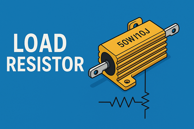 Load Resistor: Principles, Calculation and LED Applications
23 July 20254458
 Why Precision Matters in Analog-to-Digital Conversion
28 May 2025934
 Difference between Various Motors and How to Select a Motor?
10 January 20224851
 Operational Amplifier Basics: Working Principle and Amplifier Circuit
21 March 202520930
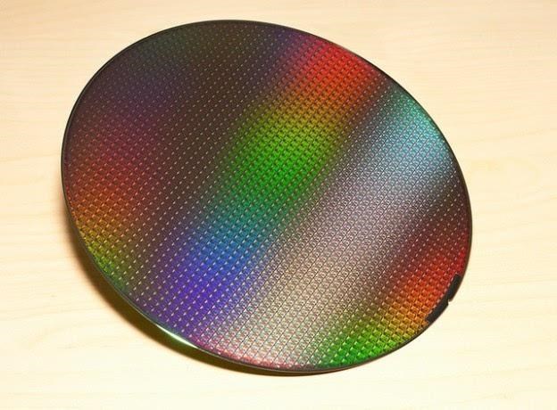 Analysis of Semiconductor Wafers
22 October 202516581
 What is an Operational Amplifier?
27 March 20253873
RAYTHEON SEMICONDUCTOR
In Stock
United States
China
Canada
Japan
Russia
Germany
United Kingdom
Singapore
Italy
Hong Kong(China)
Taiwan(China)
France
Korea
Mexico
Netherlands
Malaysia
Austria
Spain
Switzerland
Poland
Thailand
Vietnam
India
United Arab Emirates
Afghanistan
Åland Islands
Albania
Algeria
American Samoa
Andorra
Angola
Anguilla
Antigua & Barbuda
Argentina
Armenia
Aruba
Australia
Azerbaijan
Bahamas
Bahrain
Bangladesh
Barbados
Belarus
Belgium
Belize
Benin
Bermuda
Bhutan
Bolivia
Bonaire, Sint Eustatius and Saba
Bosnia & Herzegovina
Botswana
Brazil
British Indian Ocean Territory
British Virgin Islands
Brunei
Bulgaria
Burkina Faso
Burundi
Cabo Verde
Cambodia
Cameroon
Cayman Islands
Central African Republic
Chad
Chile
Christmas Island
Cocos (Keeling) Islands
Colombia
Comoros
Congo
Congo (DRC)
Cook Islands
Costa Rica
Côte d’Ivoire
Croatia
Cuba
Curaçao
Cyprus
Czechia
Denmark
Djibouti
Dominica
Dominican Republic
Ecuador
Egypt
El Salvador
Equatorial Guinea
Eritrea
Estonia
Eswatini
Ethiopia
Falkland Islands
Faroe Islands
Fiji
Finland
French Guiana
French Polynesia
Gabon
Gambia
Georgia
Ghana
Gibraltar
Greece
Greenland
Grenada
Guadeloupe
Guam
Guatemala
Guernsey
Guinea
Guinea-Bissau
Guyana
Haiti
Honduras
Hungary
Iceland
Indonesia
Iran
Iraq
Ireland
Isle of Man
Israel
Jamaica
Jersey
Jordan
Kazakhstan
Kenya
Kiribati
Kosovo
Kuwait
Kyrgyzstan
Laos
Latvia
Lebanon
Lesotho
Liberia
Libya
Liechtenstein
Lithuania
Luxembourg
Macao(China)
Madagascar
Malawi
Maldives
Mali
Malta
Marshall Islands
Martinique
Mauritania
Mauritius
Mayotte
Micronesia
Moldova
Monaco
Mongolia
Montenegro
Montserrat
Morocco
Mozambique
Myanmar
Namibia
Nauru
Nepal
New Caledonia
New Zealand
Nicaragua
Niger
Nigeria
Niue
Norfolk Island
North Korea
North Macedonia
Northern Mariana Islands
Norway
Oman
Pakistan
Palau
Palestinian Authority
Panama
Papua New Guinea
Paraguay
Peru
Philippines
Pitcairn Islands
Portugal
Puerto Rico
Qatar
Réunion
Romania
Rwanda
Samoa
San Marino
São Tomé & Príncipe
Saudi Arabia
Senegal
Serbia
Seychelles
Sierra Leone
Sint Maarten
Slovakia
Slovenia
Solomon Islands
Somalia
South Africa
South Sudan
Sri Lanka
St Helena, Ascension, Tristan da Cunha
St. Barthélemy
St. Kitts & Nevis
St. Lucia
St. Martin
St. Pierre & Miquelon
St. Vincent & Grenadines
Sudan
Suriname
Svalbard & Jan Mayen
Sweden
Syria
Tajikistan
Tanzania
Timor-Leste
Togo
Tokelau
Tonga
Trinidad & Tobago
Tunisia
Turkey
Turkmenistan
Turks & Caicos Islands
Tuvalu
U.S. Outlying Islands
U.S. Virgin Islands
Uganda
Ukraine
Uruguay
Uzbekistan
Vanuatu
Vatican City
Venezuela
Wallis & Futuna
Yemen
Zambia
Zimbabwe