
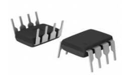
AO3401A P-Channel 30V Fast Switching MOSFETs, 4A SOT23 and AO3401A Equivalents

Alpha & Omega Semiconductor Inc.
P-Channel Cut Tape (CT) 44m Ω @ 4.3A, 10V ±12V 1200pF @ 15V 12.2nC @ 4.5V 30V TO-236-3, SC-59, SOT-23-3


P-Channel Cut Tape (CT) 44m Ω @ 4.3A, 10V ±12V 1200pF @ 15V 12.2nC @ 4.5V 30V TO-236-3, SC-59, SOT-23-3
The AO3401A is the high cell density trenched P-channel MOSFETs, which provides excellent RDSON and efficiency for most of the small power switching and load switch applications. This article is going to discuss many details about AO3401A MOSFET.
An overview of AO3401A
The AO3401A is the high cell density trenched P-channel MOSFETs, which provides excellent RDSON and efficiency for most of the small power switching and load switch applications. The AO3401A meets the RoHS and Green Product requirement with full function reliability approved.
AO3401A Pinout

AO3401A Pinout
AO3401A CAD Model

AO3401A Symbol

AO3401A Footprint

AO3401A 3D Model
Specifications
- TypeParameter
- Mount
In electronic components, the term "Mount" typically refers to the method or process of physically attaching or fixing a component onto a circuit board or other electronic device. This can involve soldering, adhesive bonding, or other techniques to secure the component in place. The mounting process is crucial for ensuring proper electrical connections and mechanical stability within the electronic system. Different components may have specific mounting requirements based on their size, shape, and function, and manufacturers provide guidelines for proper mounting procedures to ensure optimal performance and reliability of the electronic device.
Surface Mount - Mounting Type
The "Mounting Type" in electronic components refers to the method used to attach or connect a component to a circuit board or other substrate, such as through-hole, surface-mount, or panel mount.
Surface Mount - Package / Case
refers to the protective housing that encases an electronic component, providing mechanical support, electrical connections, and thermal management.
TO-236-3, SC-59, SOT-23-3 - Number of Pins3
- Transistor Element Material
The "Transistor Element Material" parameter in electronic components refers to the material used to construct the transistor within the component. Transistors are semiconductor devices that amplify or switch electronic signals and are a fundamental building block in electronic circuits. The material used for the transistor element can significantly impact the performance and characteristics of the component. Common materials used for transistor elements include silicon, germanium, and gallium arsenide, each with its own unique properties and suitability for different applications. The choice of transistor element material is crucial in designing electronic components to meet specific performance requirements such as speed, power efficiency, and temperature tolerance.
SILICON - Current - Continuous Drain (Id) @ 25℃4A Ta
- Drive Voltage (Max Rds On, Min Rds On)2.5V 10V
- Number of Elements1
- Power Dissipation (Max)1.4W Ta
- Turn Off Delay Time
It is the time from when Vgs drops below 90% of the gate drive voltage to when the drain current drops below 90% of the load current. It is the delay before current starts to transition in the load, and depends on Rg. Ciss.
41 ns - Operating Temperature
The operating temperature is the range of ambient temperature within which a power supply, or any other electrical equipment, operate in. This ranges from a minimum operating temperature, to a peak or maximum operating temperature, outside which, the power supply may fail.
-55°C~150°C TJ - Packaging
Semiconductor package is a carrier / shell used to contain and cover one or more semiconductor components or integrated circuits. The material of the shell can be metal, plastic, glass or ceramic.
Cut Tape (CT) - Published2011
- Pbfree Code
The "Pbfree Code" parameter in electronic components refers to the code or marking used to indicate that the component is lead-free. Lead (Pb) is a toxic substance that has been widely used in electronic components for many years, but due to environmental concerns, there has been a shift towards lead-free alternatives. The Pbfree Code helps manufacturers and users easily identify components that do not contain lead, ensuring compliance with regulations and promoting environmentally friendly practices. It is important to pay attention to the Pbfree Code when selecting electronic components to ensure they meet the necessary requirements for lead-free applications.
yes - Part Status
Parts can have many statuses as they progress through the configuration, analysis, review, and approval stages.
Not For New Designs - Moisture Sensitivity Level (MSL)
Moisture Sensitivity Level (MSL) is a standardized rating that indicates the susceptibility of electronic components, particularly semiconductors, to moisture-induced damage during storage and the soldering process, defining the allowable exposure time to ambient conditions before they require special handling or baking to prevent failures
1 (Unlimited) - Number of Terminations3
- ECCN Code
An ECCN (Export Control Classification Number) is an alphanumeric code used by the U.S. Bureau of Industry and Security to identify and categorize electronic components and other dual-use items that may require an export license based on their technical characteristics and potential for military use.
EAR99 - Terminal Position
In electronic components, the term "Terminal Position" refers to the physical location of the connection points on the component where external electrical connections can be made. These connection points, known as terminals, are typically used to attach wires, leads, or other components to the main body of the electronic component. The terminal position is important for ensuring proper connectivity and functionality of the component within a circuit. It is often specified in technical datasheets or component specifications to help designers and engineers understand how to properly integrate the component into their circuit designs.
DUAL - Terminal Form
Occurring at or forming the end of a series, succession, or the like; closing; concluding.
GULL WING - Pin Count
a count of all of the component leads (or pins)
3 - Configuration
The parameter "Configuration" in electronic components refers to the specific arrangement or setup of the components within a circuit or system. It encompasses how individual elements are interconnected and their physical layout. Configuration can affect the functionality, performance, and efficiency of the electronic system, and may influence factors such as signal flow, impedance, and power distribution. Understanding the configuration is essential for design, troubleshooting, and optimizing electronic devices.
SINGLE WITH BUILT-IN DIODE - Number of Channels1
- Operating Mode
A phase of operation during the operation and maintenance stages of the life cycle of a facility.
ENHANCEMENT MODE - Power Dissipation
the process by which an electronic or electrical device produces heat (energy loss or waste) as an undesirable derivative of its primary action.
1.4W - Turn On Delay Time
Turn-on delay, td(on), is the time taken to charge the input capacitance of the device before drain current conduction can start.
6.5 ns - FET Type
"FET Type" refers to the type of Field-Effect Transistor (FET) being used in an electronic component. FETs are three-terminal semiconductor devices that can be classified into different types based on their construction and operation. The main types of FETs include Metal-Oxide-Semiconductor FETs (MOSFETs), Junction FETs (JFETs), and Insulated-Gate Bipolar Transistors (IGBTs).Each type of FET has its own unique characteristics and applications. MOSFETs are commonly used in digital circuits due to their high input impedance and low power consumption. JFETs are often used in low-noise amplifiers and switching circuits. IGBTs combine the high input impedance of MOSFETs with the high current-carrying capability of bipolar transistors, making them suitable for high-power applications like motor control and power inverters.When selecting an electronic component, understanding the FET type is crucial as it determines the device's performance and suitability for a specific application. It is important to consider factors such as voltage ratings, current handling capabilities, switching speeds, and power dissipation when choosing the right FET type for a particular circuit design.
P-Channel - Transistor Application
In the context of electronic components, the parameter "Transistor Application" refers to the specific purpose or function for which a transistor is designed and used. Transistors are semiconductor devices that can amplify or switch electronic signals and are commonly used in various electronic circuits. The application of a transistor can vary widely depending on its design and characteristics, such as whether it is intended for audio amplification, digital logic, power control, or radio frequency applications. Understanding the transistor application is important for selecting the right type of transistor for a particular circuit or system to ensure optimal performance and functionality.
SWITCHING - Rds On (Max) @ Id, Vgs
Rds On (Max) @ Id, Vgs refers to the maximum on-resistance of a MOSFET or similar transistor when it is fully turned on or in the saturation region. It is specified at a given drain current (Id) and gate-source voltage (Vgs). This parameter indicates how much resistance the component will offer when conducting, impacting power loss and efficiency in a circuit. Lower Rds On values are preferred for better performance in switching applications.
44m Ω @ 4.3A, 10V - Vgs(th) (Max) @ Id
The parameter "Vgs(th) (Max) @ Id" in electronic components refers to the maximum gate-source threshold voltage at a specified drain current (Id). This parameter is commonly found in field-effect transistors (FETs) and is used to define the minimum voltage required at the gate terminal to turn on the transistor and allow current to flow from the drain to the source. The maximum value indicates the upper limit of this threshold voltage under specified operating conditions. It is an important parameter for determining the proper biasing and operating conditions of the FET in a circuit to ensure proper functionality and performance.
1.3V @ 250μA - Input Capacitance (Ciss) (Max) @ Vds
The parameter "Input Capacitance (Ciss) (Max) @ Vds" in electronic components refers to the maximum input capacitance measured at a specific drain-source voltage (Vds). Input capacitance is a crucial parameter in field-effect transistors (FETs) and power MOSFETs, as it represents the total capacitance at the input terminal of the device. This capacitance affects the device's switching speed and overall performance, as it influences the time required for charging and discharging during operation. Manufacturers provide this parameter to help designers understand the device's input characteristics and make informed decisions when integrating it into a circuit.
1200pF @ 15V - Gate Charge (Qg) (Max) @ Vgs
Gate Charge (Qg) (Max) @ Vgs refers to the maximum amount of charge that must be supplied to the gate of a MOSFET or similar device to fully turn it on, measured at a specific gate-source voltage (Vgs). This parameter is crucial for understanding the switching characteristics of the device, as it influences the speed at which the gate can charge and discharge. A higher gate charge value often implies slower switching speeds, which can impact the efficiency of high-frequency applications. This parameter is typically specified in nanocoulombs (nC) in the component's datasheet.
12.2nC @ 4.5V - Drain to Source Voltage (Vdss)
The Drain to Source Voltage (Vdss) is a key parameter in electronic components, particularly in field-effect transistors (FETs) such as MOSFETs. It refers to the maximum voltage that can be applied between the drain and source terminals of the FET without causing damage to the component. Exceeding this voltage limit can lead to breakdown and potentially permanent damage to the device.Vdss is an important specification to consider when designing or selecting components for a circuit, as it determines the operating range and reliability of the FET. It is crucial to ensure that the Vdss rating of the component is higher than the maximum voltage expected in the circuit to prevent failures and ensure proper functionality.In summary, the Drain to Source Voltage (Vdss) is a critical parameter that defines the maximum voltage tolerance of a FET component and plays a significant role in determining the overall performance and reliability of electronic circuits.
30V - Vgs (Max)
Vgs (Max) refers to the maximum gate-source voltage that can be applied to a field-effect transistor (FET) without causing damage to the component. This parameter is crucial in determining the safe operating limits of the FET and helps prevent overvoltage conditions that could lead to device failure. Exceeding the specified Vgs (Max) rating can result in breakdown of the gate oxide layer, leading to permanent damage to the FET. Designers must ensure that the applied gate-source voltage does not exceed the maximum rating to ensure reliable and long-term operation of the electronic component.
±12V - Continuous Drain Current (ID)
Continuous Drain Current (ID) is a key parameter in electronic components, particularly in field-effect transistors (FETs) such as MOSFETs. It refers to the maximum current that can flow continuously through the drain terminal of the FET without causing damage to the component. This parameter is crucial for determining the power handling capability of the FET and is specified by the manufacturer in the component's datasheet. Designers must ensure that the actual operating current does not exceed the specified Continuous Drain Current to prevent overheating and potential failure of the component.
-4A - Threshold Voltage
The threshold voltage is a critical parameter in electronic components, particularly in field-effect transistors (FETs). It refers to the minimum voltage required at the input terminal of the FET to turn it on and allow current to flow between the source and drain terminals. Below the threshold voltage, the FET remains in the off state, acting as an open switch. Once the threshold voltage is exceeded, the FET enters the on state, conducting current between the source and drain.The threshold voltage is a key factor in determining the operating characteristics of FETs, such as their switching speed and power consumption. It is typically specified by the manufacturer and can vary depending on the specific type of FET and its design. Designers must consider the threshold voltage when selecting FETs for a particular application to ensure proper functionality and performance.
-900mV - Gate to Source Voltage (Vgs)
The Gate to Source Voltage (Vgs) is a crucial parameter in electronic components, particularly in field-effect transistors (FETs) such as MOSFETs. It refers to the voltage difference between the gate and source terminals of the FET. This voltage determines the conductivity of the FET and controls the flow of current through the device. By varying the Vgs, the FET can be switched on or off, allowing for precise control of electronic circuits. Understanding and properly managing the Vgs is essential for ensuring the reliable and efficient operation of FET-based circuits.
12V - Drain Current-Max (Abs) (ID)
The parameter "Drain Current-Max (Abs) (ID)" in electronic components refers to the maximum current that can flow from the drain to the source terminal of a field-effect transistor (FET) or a similar device. It is a crucial specification that indicates the maximum current handling capability of the component before it reaches its saturation point or gets damaged. This parameter is typically specified in amperes (A) and helps designers ensure that the component can safely handle the expected current levels in a circuit without exceeding its limits. It is important to consider this parameter when designing circuits to prevent overloading the component and ensure reliable operation.
4A - Drain-source On Resistance-Max
Drain-source On Resistance-Max, commonly referred to as RDS(on) max, is a specification for MOSFETs that indicates the maximum resistance between the drain and source terminals when the device is turned on. This parameter is critical for assessing the efficiency of a MOSFET in a circuit, as lower values result in reduced power loss and heat generation during operation. It is measured in ohms and is influenced by factors such as temperature and gate-to-source voltage. Understanding RDS(on) max is essential for optimizing performance in power management and switching applications.
0.05Ohm - Drain to Source Breakdown Voltage
Drain to Source Breakdown Voltage, often denoted as V(BR) D-S, is a critical parameter in electronic components, particularly in field-effect transistors (FETs) and metal-oxide-semiconductor FETs (MOSFETs). It represents the maximum voltage that can be applied between the drain and source terminals of the device without causing breakdown or permanent damage. Exceeding this voltage can lead to excessive current flow, resulting in thermal failure or destruction of the component. It is essential for ensuring reliable operation in circuit designs where high voltages may be encountered.
-30V - Max Junction Temperature (Tj)
Max Junction Temperature (Tj) refers to the maximum allowable temperature at the junction of a semiconductor device, such as a transistor or integrated circuit. It is a critical parameter that influences the performance, reliability, and lifespan of the component. Exceeding this temperature can lead to thermal runaway, breakdown, or permanent damage to the device. Proper thermal management is essential to ensure the junction temperature remains within safe operating limits during device operation.
150°C - Height1.25mm
- Radiation Hardening
Radiation hardening is the process of making electronic components and circuits resistant to damage or malfunction caused by high levels of ionizing radiation, especially for environments in outer space (especially beyond the low Earth orbit), around nuclear reactors and particle accelerators, or during nuclear accidents or nuclear warfare.
No - RoHS Status
RoHS means “Restriction of Certain Hazardous Substances” in the “Hazardous Substances Directive” in electrical and electronic equipment.
ROHS3 Compliant - Lead Free
Lead Free is a term used to describe electronic components that do not contain lead as part of their composition. Lead is a toxic material that can have harmful effects on human health and the environment, so the electronics industry has been moving towards lead-free components to reduce these risks. Lead-free components are typically made using alternative materials such as silver, copper, and tin. Manufacturers must comply with regulations such as the Restriction of Hazardous Substances (RoHS) directive to ensure that their products are lead-free and environmentally friendly.
Lead Free
AO3401A Features
Type of Transistor: MOSFET
Type of Control Channel: P -Channel
Maximum Power Dissipation (Pd): 1.4 W
Maximum Drain-Source Voltage |Vds|: 30 V
Maximum Gate-Source Voltage |Vgs|: 12 V
Maximum Gate-Threshold Voltage |Vgs(th)|: 1.3 V
Maximum Drain Current |Id|: 4 A
Maximum Junction Temperature (Tj): 150 °C
Rise Time (tr): 3.5 nS
Drain-Source Capacitance (Cd): 80 pF
Maximum Drain-Source On-State Resistance (Rds): 0.05 Ohm
Package: SOT23
AO3401A Benefits
Gull Wing style lead
Surface Mounting
Fast Switching
Green Device Available
Super Low Gate Charge
Excellent CdV/dt effect decline
Advanced high cell density Trench technology
AO3401A Applications
Industrial uses
Domestic uses
AO3401A Test Circuit


AO3401A Test Circuit
Where to use AO3401A
AO3401A is suitable for use as a load switch or other general applications. This P-channel MOSFET transistor operates in enhancement mode. Its maximum power dissipation is 1400 mW. The maximum Drain Source Voltage of the product is 30 V and Gate Source Voltage is ±12 V. This MOSFET has an operating temperature range of -55°C to 150°C.
AO3401A Alternatives
2SJ600-Z , 2SJ602-ZJ , 2SJ603-ZJ , 2SJ604-ZJ , 2SJ605-ZJ , 2SJ606-ZJ , 2SJ607-ZJ , A9451 , IRF460 , AO3415AS , AO3415W , AO4335 , AO4705 , AOD413 , BSL211DV , DMP1260 , FQD12P10
Parts with Similar Specs
- ImagePart NumberManufacturerMountPackage / CaseDrain to Source Voltage (Vdss)Continuous Drain Current (ID)Current - Continuous Drain (Id) @ 25°CThreshold VoltageGate to Source Voltage (Vgs)Power DissipationView Compare
![AO3401A]()
AO3401A
Surface Mount
TO-236-3, SC-59, SOT-23-3
30V
-4 A
4A (Ta)
-900 mV
12 V
1.4 W
![IRLML6344TRPBF]()
Surface Mount
TO-236-3, SC-59, SOT-23-3
30V
4.2 A
4.2A (Ta)
-
20 V
-
![IRLML6346TRPBF]()
Surface Mount
TO-236-3, SC-59, SOT-23-3
-
5 A
5A (Ta)
800 mV
12 V
1.3 W
![DMP3056L-7]()
Surface Mount
TO-236-3, SC-59, SOT-23-3
-
3.4 A
3.4A (Ta)
800 mV
12 V
1.3 W
![DMN3070SSN-7]()
Surface Mount
TO-236-3, SC-59, SOT-23-3
30V
-4.3 A
4.3A (Ta)
-
25 V
1.38 W


AO3401A Dimensions


AO3401A Dimensions
AO3401A Manufacturer
Alpha and Omega Semiconductor, Inc., or AOS, is a designer, developer, and global supplier of a broad range of power semiconductors, including a wide portfolio of Power MOSFET and Power IC products. AOS seeks to differentiate itself by integrating its expertise in device physics, process technology, design, and advanced packaging to optimize product performance and cost, and its product portfolio is designed to meet the ever-increasing power efficiency requirements in high volume applications, including portable computers, flat-panel TVs, battery packs, portable media players and power supplies.
Similar parts from Alpha and Omega Semiconductor, Inc. are as follows: ao3401, ao3400, ao3400a, ao3415, etc.
Trend Analysis
What is the maximum Drain Source Voltage of AO3401A?
30 V
What is the maximum power dissipation of AO3401A?
1400 mW
What mode does the P channel MOSFET transistor operate in?
The enhancement mode
What is the use of AO3401A?
AO3401A is suitable for use as a load switch or other general applications. This P channel MOSFET transistor operates in enhancement mode. Its maximum power dissipation is 1400 mW.
 M95M01-R EEPROM: Pinout, Equivalent and Datasheet
20 December 20212199
 LME49720 Audio Operational Amplifier: Circuit, Price and Alternatives
29 June 20214211
 MPSA42 NPN Transistor: Pinout, Datasheet and Replacement
12 October 202111494
 ADALM2000 Analog Device: Advanced Active Learning Module USB
11 January 20221692
 LM3914N Display Driver: Datasheet, Pinout and Comparison
02 August 20216079
 AD210AN Isolation Amplifier: Pinout, Functions, Datasheet
24 October 20221463
 MTFC8GAKAJCN-4M IT Flash Card 8G-byte 3.3V 153-Pin VFBGA: Datasheet, Pinout, and Equivalents
14 February 20221958
 TC4420 MOSFET Driver: Datasheet, Pinout, Application Circuit
13 December 202111688
 Real-time Cloud Analytics in Semiconductor Manufacturing
01 November 20221147
 Yahoo Discontinues Services in Mainland China
13 November 2023799
 Network Interface Card: Types, Functions and Buying Guide
17 August 20218245
 Reed Relays: 10 Key Applications in Modern Electronics
04 July 2025588
 How to Address IoT Eco-security in the Era of Digital Transformation?
22 April 2022493
 Will AI Eventually Compete With Humans for Energy Resources?
14 February 20232719
 Apple Will Help TSMC to Be in the Leading Position in the Next Era
16 March 20221973
 Designing Application-Specific Integrated Circuits
07 March 20251579
Alpha & Omega Semiconductor Inc.
In Stock: 9390
United States
China
Canada
Japan
Russia
Germany
United Kingdom
Singapore
Italy
Hong Kong(China)
Taiwan(China)
France
Korea
Mexico
Netherlands
Malaysia
Austria
Spain
Switzerland
Poland
Thailand
Vietnam
India
United Arab Emirates
Afghanistan
Åland Islands
Albania
Algeria
American Samoa
Andorra
Angola
Anguilla
Antigua & Barbuda
Argentina
Armenia
Aruba
Australia
Azerbaijan
Bahamas
Bahrain
Bangladesh
Barbados
Belarus
Belgium
Belize
Benin
Bermuda
Bhutan
Bolivia
Bonaire, Sint Eustatius and Saba
Bosnia & Herzegovina
Botswana
Brazil
British Indian Ocean Territory
British Virgin Islands
Brunei
Bulgaria
Burkina Faso
Burundi
Cabo Verde
Cambodia
Cameroon
Cayman Islands
Central African Republic
Chad
Chile
Christmas Island
Cocos (Keeling) Islands
Colombia
Comoros
Congo
Congo (DRC)
Cook Islands
Costa Rica
Côte d’Ivoire
Croatia
Cuba
Curaçao
Cyprus
Czechia
Denmark
Djibouti
Dominica
Dominican Republic
Ecuador
Egypt
El Salvador
Equatorial Guinea
Eritrea
Estonia
Eswatini
Ethiopia
Falkland Islands
Faroe Islands
Fiji
Finland
French Guiana
French Polynesia
Gabon
Gambia
Georgia
Ghana
Gibraltar
Greece
Greenland
Grenada
Guadeloupe
Guam
Guatemala
Guernsey
Guinea
Guinea-Bissau
Guyana
Haiti
Honduras
Hungary
Iceland
Indonesia
Iran
Iraq
Ireland
Isle of Man
Israel
Jamaica
Jersey
Jordan
Kazakhstan
Kenya
Kiribati
Kosovo
Kuwait
Kyrgyzstan
Laos
Latvia
Lebanon
Lesotho
Liberia
Libya
Liechtenstein
Lithuania
Luxembourg
Macao(China)
Madagascar
Malawi
Maldives
Mali
Malta
Marshall Islands
Martinique
Mauritania
Mauritius
Mayotte
Micronesia
Moldova
Monaco
Mongolia
Montenegro
Montserrat
Morocco
Mozambique
Myanmar
Namibia
Nauru
Nepal
New Caledonia
New Zealand
Nicaragua
Niger
Nigeria
Niue
Norfolk Island
North Korea
North Macedonia
Northern Mariana Islands
Norway
Oman
Pakistan
Palau
Palestinian Authority
Panama
Papua New Guinea
Paraguay
Peru
Philippines
Pitcairn Islands
Portugal
Puerto Rico
Qatar
Réunion
Romania
Rwanda
Samoa
San Marino
São Tomé & Príncipe
Saudi Arabia
Senegal
Serbia
Seychelles
Sierra Leone
Sint Maarten
Slovakia
Slovenia
Solomon Islands
Somalia
South Africa
South Sudan
Sri Lanka
St Helena, Ascension, Tristan da Cunha
St. Barthélemy
St. Kitts & Nevis
St. Lucia
St. Martin
St. Pierre & Miquelon
St. Vincent & Grenadines
Sudan
Suriname
Svalbard & Jan Mayen
Sweden
Syria
Tajikistan
Tanzania
Timor-Leste
Togo
Tokelau
Tonga
Trinidad & Tobago
Tunisia
Turkey
Turkmenistan
Turks & Caicos Islands
Tuvalu
U.S. Outlying Islands
U.S. Virgin Islands
Uganda
Ukraine
Uruguay
Uzbekistan
Vanuatu
Vatican City
Venezuela
Wallis & Futuna
Yemen
Zambia
Zimbabwe
![AON6562]() AON6562
AON6562Alpha & Omega Semiconductor Inc.
![AOL1428]() AOL1428
AOL1428Alpha & Omega Semiconductor Inc.
![AON6912ALS]() AON6912ALS
AON6912ALSAlpha & Omega Semiconductor Inc.
![AO4722]() AO4722
AO4722Alpha & Omega Semiconductor Inc.
![AO3422]() AO3422
AO3422Alpha & Omega Semiconductor Inc.
![AO3419]() AO3419
AO3419Alpha & Omega Semiconductor Inc.
![AOD458]() AOD458
AOD458Alpha & Omega Semiconductor Inc.
![AO4459]() AO4459
AO4459Alpha & Omega Semiconductor Inc.
![AO3400A]() AO3400A
AO3400AAlpha & Omega Semiconductor Inc.


