
 Product
 Brand
Brand Articles
 Tools
Tools
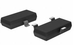
S9012 Transistor: BJT Transistor, Datasheet, Equivalent


SMALL SIGNAL BIPOLAR TRANSISTOR
SS9012 is a BJT transistor manufactured in the TO-92 package, it is also used in many commercial electronic appliances and devices. This article covers its pinout, datasheet, equivalent and more details about SS9012. Welcome your RFQ!
SS9012 Pinout

SS9012 Pinout
SS9012 CAD Model
Symbol

SS9012 Symbol
Footprint

SS9012 Footprint
3D Model

SS9012 3D Model
SS9012 Description
The SS9012 is a BJT transistor with a TO-92 package that can be found in a variety of commercial electronic appliances and gadgets. The transistor can be used for a variety of purposes, but according to the manufacturer, it is primarily designed for audio amplification and can be used as a 1000mW amplifier for any device that outputs a few milliwatts of audio. The SS9012, like other general-purpose transistors such as the 2N3906, 2N4403, and BC559, can be utilized in a wide range of electronics applications, and it is also a must-have transistor in the electronic lab. Aside from that, this transistor can be used as a switch to drive loads that draw less than 500 milliamps.
SS9012 Feature
• High total power dissipation. (PT=625mW)
• High Collector Current. (IC= -500mA)
• Complementary to SS9013
• Excellent hFE linearity
SS9012 Application
The output of Microcontrollers to Drive Loads
Audio amplifier
Any Signal Amplification
Drive Load Under 500mA
Audio Amplifier Stages
SS9012 Equivalent
The equivalent for SS9012:
S8550
BC328
2N4403
Where to Use SS9012 Transistor?
As previously stated, the SS9012 is a general-purpose PNP BJT transistor that can be employed in a wide range of applications. It can, for example, be used as an audio amplifier to drive a 1-watt speaker directly. It can also be employed in the audio amplifier circuit's amplification stages. This transistor can drive a range of loads, including relays, high-power transistors, ICs, and LEDs, thanks to its 500mA or 0.5A load driving capacity. It can also be utilized at the output of microcontrollers to drive loads under 500mA with a -5V emitter-base voltage (VBE). It can also be used to replace a variety of other common-purpose transistors.
How to Get Long Term Performance?
To obtain the best long-term performance out of the SS9012 transistor, it's best to keep the load at 500mA and not to operate it at more than 20V. With the transistor, use a sufficient base resistor. Always double-check pin configuration before putting the transistor in the circuit, and store or operate the transistor at temperatures between -55 and +150 ℃.
Specifications
- TypeParameter
- Mounting Type
The "Mounting Type" in electronic components refers to the method used to attach or connect a component to a circuit board or other substrate, such as through-hole, surface-mount, or panel mount.
Through Hole - Package / Case
refers to the protective housing that encases an electronic component, providing mechanical support, electrical connections, and thermal management.
TO-226-3, TO-92-3 (TO-226AA) (Formed Leads) - Surface Mount
having leads that are designed to be soldered on the side of a circuit board that the body of the component is mounted on.
NO - Transistor Element Material
The "Transistor Element Material" parameter in electronic components refers to the material used to construct the transistor within the component. Transistors are semiconductor devices that amplify or switch electronic signals and are a fundamental building block in electronic circuits. The material used for the transistor element can significantly impact the performance and characteristics of the component. Common materials used for transistor elements include silicon, germanium, and gallium arsenide, each with its own unique properties and suitability for different applications. The choice of transistor element material is crucial in designing electronic components to meet specific performance requirements such as speed, power efficiency, and temperature tolerance.
SILICON - Current-Collector (Ic) (Max)500mA
- Number of Elements1
- Operating Temperature
The operating temperature is the range of ambient temperature within which a power supply, or any other electrical equipment, operate in. This ranges from a minimum operating temperature, to a peak or maximum operating temperature, outside which, the power supply may fail.
150°C TJ - Packaging
Semiconductor package is a carrier / shell used to contain and cover one or more semiconductor components or integrated circuits. The material of the shell can be metal, plastic, glass or ceramic.
Tape & Box (TB) - JESD-609 Code
The "JESD-609 Code" in electronic components refers to a standardized marking code that indicates the lead-free solder composition and finish of electronic components for compliance with environmental regulations.
e3 - Pbfree Code
The "Pbfree Code" parameter in electronic components refers to the code or marking used to indicate that the component is lead-free. Lead (Pb) is a toxic substance that has been widely used in electronic components for many years, but due to environmental concerns, there has been a shift towards lead-free alternatives. The Pbfree Code helps manufacturers and users easily identify components that do not contain lead, ensuring compliance with regulations and promoting environmentally friendly practices. It is important to pay attention to the Pbfree Code when selecting electronic components to ensure they meet the necessary requirements for lead-free applications.
yes - Part Status
Parts can have many statuses as they progress through the configuration, analysis, review, and approval stages.
Obsolete - Moisture Sensitivity Level (MSL)
Moisture Sensitivity Level (MSL) is a standardized rating that indicates the susceptibility of electronic components, particularly semiconductors, to moisture-induced damage during storage and the soldering process, defining the allowable exposure time to ambient conditions before they require special handling or baking to prevent failures
1 (Unlimited) - Number of Terminations3
- Terminal Finish
Terminal Finish refers to the surface treatment applied to the terminals or leads of electronic components to enhance their performance and longevity. It can improve solderability, corrosion resistance, and overall reliability of the connection in electronic assemblies. Common finishes include nickel, gold, and tin, each possessing distinct properties suitable for various applications. The choice of terminal finish can significantly impact the durability and effectiveness of electronic devices.
MATTE TIN - Terminal Position
In electronic components, the term "Terminal Position" refers to the physical location of the connection points on the component where external electrical connections can be made. These connection points, known as terminals, are typically used to attach wires, leads, or other components to the main body of the electronic component. The terminal position is important for ensuring proper connectivity and functionality of the component within a circuit. It is often specified in technical datasheets or component specifications to help designers and engineers understand how to properly integrate the component into their circuit designs.
BOTTOM - Peak Reflow Temperature (Cel)
Peak Reflow Temperature (Cel) is a parameter that specifies the maximum temperature at which an electronic component can be exposed during the reflow soldering process. Reflow soldering is a common method used to attach electronic components to a circuit board. The Peak Reflow Temperature is crucial because it ensures that the component is not damaged or degraded during the soldering process. Exceeding the specified Peak Reflow Temperature can lead to issues such as component failure, reduced performance, or even permanent damage to the component. It is important for manufacturers and assemblers to adhere to the recommended Peak Reflow Temperature to ensure the reliability and functionality of the electronic components.
NOT APPLICABLE - Time@Peak Reflow Temperature-Max (s)
Time@Peak Reflow Temperature-Max (s) refers to the maximum duration that an electronic component can be exposed to the peak reflow temperature during the soldering process, which is crucial for ensuring reliable solder joint formation without damaging the component.
NOT APPLICABLE - JESD-30 Code
JESD-30 Code refers to a standardized descriptive designation system established by JEDEC for semiconductor-device packages. This system provides a systematic method for generating designators that convey essential information about the package's physical characteristics, such as size and shape, which aids in component identification and selection. By using JESD-30 codes, manufacturers and engineers can ensure consistency and clarity in the specification of semiconductor packages across various applications and industries.
O-PBCY-T3 - Qualification Status
An indicator of formal certification of qualifications.
COMMERCIAL - Configuration
The parameter "Configuration" in electronic components refers to the specific arrangement or setup of the components within a circuit or system. It encompasses how individual elements are interconnected and their physical layout. Configuration can affect the functionality, performance, and efficiency of the electronic system, and may influence factors such as signal flow, impedance, and power distribution. Understanding the configuration is essential for design, troubleshooting, and optimizing electronic devices.
SINGLE - Power - Max
Power - Max is a parameter that specifies the maximum amount of power that an electronic component can handle without being damaged. It is typically measured in watts and indicates the upper limit of power that can be safely supplied to the component. Exceeding the maximum power rating can lead to overheating, malfunction, or permanent damage to the component. It is important to consider the power-max rating when designing circuits or systems to ensure proper operation and longevity of the electronic components.
625mW - Transistor Application
In the context of electronic components, the parameter "Transistor Application" refers to the specific purpose or function for which a transistor is designed and used. Transistors are semiconductor devices that can amplify or switch electronic signals and are commonly used in various electronic circuits. The application of a transistor can vary widely depending on its design and characteristics, such as whether it is intended for audio amplification, digital logic, power control, or radio frequency applications. Understanding the transistor application is important for selecting the right type of transistor for a particular circuit or system to ensure optimal performance and functionality.
AMPLIFIER - Polarity/Channel Type
In electronic components, the parameter "Polarity/Channel Type" refers to the characteristic that determines the direction of current flow or the type of signal that can be accommodated by the component. For components like diodes and transistors, polarity indicates the direction in which current can flow through the component, such as forward bias or reverse bias for diodes. For components like MOSFETs or JFETs, the channel type refers to whether the component is an N-channel or P-channel device, which determines the type of charge carriers that carry current through the component. Understanding the polarity or channel type of a component is crucial for proper circuit design and ensuring that the component is connected correctly to achieve the desired functionality.
PNP - Transistor Type
Transistor type refers to the classification of transistors based on their operation and construction. The two primary types are bipolar junction transistors (BJTs) and field-effect transistors (FETs). BJTs use current to control the flow of current, while FETs utilize voltage to control current flow. Each type has its own subtypes, such as NPN and PNP for BJTs, and MOSFETs and JFETs for FETs, impacting their applications and characteristics in electronic circuits.
PNP - DC Current Gain (hFE) (Min) @ Ic, Vce
The parameter "DC Current Gain (hFE) (Min) @ Ic, Vce" in electronic components refers to the minimum value of the DC current gain, denoted as hFE, under specific operating conditions of collector current (Ic) and collector-emitter voltage (Vce). The DC current gain hFE represents the ratio of the collector current to the base current in a bipolar junction transistor (BJT), indicating the amplification capability of the transistor. The minimum hFE value at a given Ic and Vce helps determine the transistor's performance and efficiency in amplifying signals within a circuit. Designers use this parameter to ensure proper transistor selection and performance in various electronic applications.
144 @ 50mA 1V - Current - Collector Cutoff (Max)
The parameter "Current - Collector Cutoff (Max)" refers to the maximum current at which a transistor or other electronic component will cease to conduct current between the collector and emitter terminals. This parameter is important in determining the maximum current that can flow through the component when it is in the cutoff state. Exceeding this maximum cutoff current can lead to malfunction or damage of the component. It is typically specified in the component's datasheet and is crucial for proper circuit design and operation.
100nA ICBO - Vce Saturation (Max) @ Ib, Ic
The parameter "Vce Saturation (Max) @ Ib, Ic" in electronic components refers to the maximum voltage drop across the collector-emitter junction when the transistor is in saturation mode. This parameter is specified at a certain base current (Ib) and collector current (Ic) levels. It indicates the minimum voltage required to keep the transistor fully conducting in saturation mode, ensuring that the transistor operates efficiently and does not enter the cutoff region. Designers use this parameter to ensure proper transistor operation and to prevent overheating or damage to the component.
600mV @ 50mA, 500mA - Voltage - Collector Emitter Breakdown (Max)
Voltage - Collector Emitter Breakdown (Max) is a parameter that specifies the maximum voltage that can be applied between the collector and emitter terminals of a transistor or other semiconductor device before it breaks down and allows excessive current to flow. This parameter is crucial for ensuring the safe and reliable operation of the component within its specified limits. Exceeding the maximum breakdown voltage can lead to permanent damage or failure of the device. Designers and engineers must carefully consider this parameter when selecting components for their circuits to prevent potential issues and ensure proper functionality.
20V - RoHS Status
RoHS means “Restriction of Certain Hazardous Substances” in the “Hazardous Substances Directive” in electrical and electronic equipment.
ROHS3 Compliant
SS9012 Package

SS9012 Package
SS9012 Manufacturer
Rochester Electronics is the largest continuing source manufacturer of semiconductors in the world. With product licensing from leading manufacturers such as Analog Devices, Altera, Cypress, Fairchild, Freescale, Infineon, Intel, NXP, Renesas and Texas Instruments, Rochester continues to manufacture and distribute mature products. For industrial, transportation and hi-reliability markets, this extension of the product life is critical for long term production and maintenance. With over 100,000 products and 15 billion units in stock, no other company compares to our selection, capabilities or solutions.
Datasheet PDF
- Datasheets :
What is the function of BJT?
As with all transistors, the basic function of a BJT is typically to function as a switch or to amplify, filter, and rectify power. Bipolar transistors are current-controlled and operated devices, meaning that a much smaller base current causes a larger current to flow from emitter to collector.
What is BJT and its types?
BJTs are of two types namely NPN and PNP based on doping types of the three main terminals. An NPN transistor consists of two semiconductor junctions that have a thin p-doped anode region and a PNP transistor also consists of two semiconductor junctions that have a thin n- doped cathode region.
 ATmega16: Datasheet, Pinout, and Industrial Control Guide
27 January 2026466
 TLC59116IPWR LED sink driver: Datasheet, Pinout, and Specifications
25 March 20222340
 ADS1262 ADC: Feature, Pinout and Datasheet
16 August 20246042
![EV2400 Evaluation and Demonstration Boards USB 2.0[FAQ]: Datasheet, EV2300 VS EV2400, and Features](https://res.utmel.com/Images/Article/fef602f0-bea0-4737-8ace-f64c5e9484e5.jpg) EV2400 Evaluation and Demonstration Boards USB 2.0[FAQ]: Datasheet, EV2300 VS EV2400, and Features
EV2400 Evaluation and Demonstration Boards USB 2.0[FAQ]: Datasheet, EV2300 VS EV2400, and Features28 March 20226482
 Technical Deep Dive: ADuC7030/ADuC7033 Integrated Precision Battery Sensor
29 February 2024141
 DS3232 RTC: Pinout, Datasheet and DS3232 vs. DS3231
28 March 20245268
 STM32F429IGT6: Overview, Applications, and Datasheet
18 December 20231727
 DRV5053 Hall Effect Sensor: Datasheet, Pinout and Applications
30 August 20215237
 What is RF Power Amplifier?
08 November 202511845
 What is a Knock Sensor?
08 January 202619116
 The Ultimate Guide to Maintaining Your L1154 Battery
16 June 2025869
 Google Unveils LM-Nav, A Robotic Navigation System, In Association With Universities
03 August 20224449
 Why is there a Chip Shortage?
19 October 20212625
 Enhancing the Efficiency of Semiconductors by Using the Spin of Electrons
11 February 20251455
 How to treat 5G?
23 October 20212314
 A76 Battery Equivalent Pros and Cons Explained
29 August 20252466
Rochester Electronics, LLC
In Stock
United States
China
Canada
Japan
Russia
Germany
United Kingdom
Singapore
Italy
Hong Kong(China)
Taiwan(China)
France
Korea
Mexico
Netherlands
Malaysia
Austria
Spain
Switzerland
Poland
Thailand
Vietnam
India
United Arab Emirates
Afghanistan
Åland Islands
Albania
Algeria
American Samoa
Andorra
Angola
Anguilla
Antigua & Barbuda
Argentina
Armenia
Aruba
Australia
Azerbaijan
Bahamas
Bahrain
Bangladesh
Barbados
Belarus
Belgium
Belize
Benin
Bermuda
Bhutan
Bolivia
Bonaire, Sint Eustatius and Saba
Bosnia & Herzegovina
Botswana
Brazil
British Indian Ocean Territory
British Virgin Islands
Brunei
Bulgaria
Burkina Faso
Burundi
Cabo Verde
Cambodia
Cameroon
Cayman Islands
Central African Republic
Chad
Chile
Christmas Island
Cocos (Keeling) Islands
Colombia
Comoros
Congo
Congo (DRC)
Cook Islands
Costa Rica
Côte d’Ivoire
Croatia
Cuba
Curaçao
Cyprus
Czechia
Denmark
Djibouti
Dominica
Dominican Republic
Ecuador
Egypt
El Salvador
Equatorial Guinea
Eritrea
Estonia
Eswatini
Ethiopia
Falkland Islands
Faroe Islands
Fiji
Finland
French Guiana
French Polynesia
Gabon
Gambia
Georgia
Ghana
Gibraltar
Greece
Greenland
Grenada
Guadeloupe
Guam
Guatemala
Guernsey
Guinea
Guinea-Bissau
Guyana
Haiti
Honduras
Hungary
Iceland
Indonesia
Iran
Iraq
Ireland
Isle of Man
Israel
Jamaica
Jersey
Jordan
Kazakhstan
Kenya
Kiribati
Kosovo
Kuwait
Kyrgyzstan
Laos
Latvia
Lebanon
Lesotho
Liberia
Libya
Liechtenstein
Lithuania
Luxembourg
Macao(China)
Madagascar
Malawi
Maldives
Mali
Malta
Marshall Islands
Martinique
Mauritania
Mauritius
Mayotte
Micronesia
Moldova
Monaco
Mongolia
Montenegro
Montserrat
Morocco
Mozambique
Myanmar
Namibia
Nauru
Nepal
New Caledonia
New Zealand
Nicaragua
Niger
Nigeria
Niue
Norfolk Island
North Korea
North Macedonia
Northern Mariana Islands
Norway
Oman
Pakistan
Palau
Palestinian Authority
Panama
Papua New Guinea
Paraguay
Peru
Philippines
Pitcairn Islands
Portugal
Puerto Rico
Qatar
Réunion
Romania
Rwanda
Samoa
San Marino
São Tomé & Príncipe
Saudi Arabia
Senegal
Serbia
Seychelles
Sierra Leone
Sint Maarten
Slovakia
Slovenia
Solomon Islands
Somalia
South Africa
South Sudan
Sri Lanka
St Helena, Ascension, Tristan da Cunha
St. Barthélemy
St. Kitts & Nevis
St. Lucia
St. Martin
St. Pierre & Miquelon
St. Vincent & Grenadines
Sudan
Suriname
Svalbard & Jan Mayen
Sweden
Syria
Tajikistan
Tanzania
Timor-Leste
Togo
Tokelau
Tonga
Trinidad & Tobago
Tunisia
Turkey
Turkmenistan
Turks & Caicos Islands
Tuvalu
U.S. Outlying Islands
U.S. Virgin Islands
Uganda
Ukraine
Uruguay
Uzbekistan
Vanuatu
Vatican City
Venezuela
Wallis & Futuna
Yemen
Zambia
Zimbabwe
![MMBT5551]() MMBT5551
MMBT5551Rochester Electronics, LLC
![SS8550BTA]() SS8550BTA
SS8550BTARochester Electronics, LLC
![BC846AWT1]() BC846AWT1
BC846AWT1Rochester Electronics, LLC
![BSP50E6327HTSA1]() BSP50E6327HTSA1
BSP50E6327HTSA1Rochester Electronics, LLC
![BCX6816E6327HTSA1]() BCX6816E6327HTSA1
BCX6816E6327HTSA1Rochester Electronics, LLC
![MPSA55]() MPSA55
MPSA55Rochester Electronics, LLC
![BCP49E6327HTSA1]() BCP49E6327HTSA1
BCP49E6327HTSA1Rochester Electronics, LLC
![BC559]() BC559
BC559Rochester Electronics, LLC
![BF517E6327HTSA1]() BF517E6327HTSA1
BF517E6327HTSA1Rochester Electronics, LLC
![TIP112]() TIP112
TIP112Rochester Electronics, LLC


