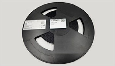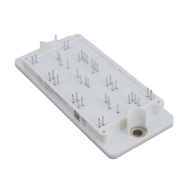

onsemi NXH600B100H4Q2F2SG
Manufacturer No:
NXH600B100H4Q2F2SG
Tiny WHSLManufacturer:
Utmel No:
1807-NXH600B100H4Q2F2SG
Package:
Module
Datasheet:
Description:
MASS MARKET GEN3 Q2BOOST
Quantity:
Unit Price: $131.399600
Ext Price: $131.40
Delivery:


Payment:


In Stock : 2200
Minimum: 1 Multiples: 1
Qty
Unit Price
Ext Price
1
$131.399600
$131.40
10
$123.961887
$1,239.62
100
$116.945176
$11,694.52
500
$110.325638
$55,162.82
1000
$104.080791
$104,080.79
Want a lower wholesale price? Please send RFQ, we will respond immediately.
RFQ Now
Add to RFQ list
You may place an order without registering to Utmel.
We strongly suggest you sign in before purchasing as you can track your order in real time.
For your convenience, we accept multiple payment methods in USD, including PayPal, Credit Card, and wire transfer.
RFQ (Request for Quotations)It is recommended to request for quotations to get the latest prices and inventories about the part.
Our sales will reply to your request by email within 24 hours.
1. You'll receive an order information email in your inbox. (Please remember to check the spam folder if you didn't hear from us).
2. Since inventories and prices may fluctuate to some extent, the sales manager is going to reconfirm the order and let you know if there are any updates.
- TypeParameter
- Mounting Type
The "Mounting Type" in electronic components refers to the method used to attach or connect a component to a circuit board or other substrate, such as through-hole, surface-mount, or panel mount.
Chassis Mount - Package / Case
refers to the protective housing that encases an electronic component, providing mechanical support, electrical connections, and thermal management.
Module - Supplier Device Package
The parameter "Supplier Device Package" in electronic components refers to the physical packaging or housing of the component as provided by the supplier. It specifies the form factor, dimensions, and layout of the component, which are crucial for compatibility and integration into electronic circuits and systems. The supplier device package information typically includes details such as the package type (e.g., DIP, SOP, QFN), number of pins, pitch, and overall size, allowing engineers and designers to select the appropriate component for their specific application requirements. Understanding the supplier device package is essential for proper component selection, placement, and soldering during the manufacturing process to ensure optimal performance and reliability of the electronic system.
44-PIM (93x47) - Current-Collector (Ic) (Max)192 A
- Base Product Number
"Base Product Number" (BPN) refers to the fundamental identifier assigned to a component by the manufacturer. This number is used to identify a specific product family or series of components that share common features, characteristics, or functionality. The BPN is usually part of a larger part number or order code that includes additional information, such as variations in packaging, tolerance, voltage ratings, and other specifications.
NXH600 - Packaging
Semiconductor package is a carrier / shell used to contain and cover one or more semiconductor components or integrated circuits. The material of the shell can be metal, plastic, glass or ceramic.
Tray - Operating Temperature
The operating temperature is the range of ambient temperature within which a power supply, or any other electrical equipment, operate in. This ranges from a minimum operating temperature, to a peak or maximum operating temperature, outside which, the power supply may fail.
-40°C ~ 175°C (TJ) - Part Status
Parts can have many statuses as they progress through the configuration, analysis, review, and approval stages.
Active - Configuration
The parameter "Configuration" in electronic components refers to the specific arrangement or setup of the components within a circuit or system. It encompasses how individual elements are interconnected and their physical layout. Configuration can affect the functionality, performance, and efficiency of the electronic system, and may influence factors such as signal flow, impedance, and power distribution. Understanding the configuration is essential for design, troubleshooting, and optimizing electronic devices.
Three Level Inverter - Power - Max
Power - Max is a parameter that specifies the maximum amount of power that an electronic component can handle without being damaged. It is typically measured in watts and indicates the upper limit of power that can be safely supplied to the component. Exceeding the maximum power rating can lead to overheating, malfunction, or permanent damage to the component. It is important to consider the power-max rating when designing circuits or systems to ensure proper operation and longevity of the electronic components.
511 W - Input
In electronic components, "Input" refers to the signal or data that is provided to a device or system for processing or manipulation. It is the information or command that is received by the component to initiate a specific function or operation. The input can come from various sources such as sensors, other electronic devices, or user interactions. It is crucial for the proper functioning of the component as it determines how the device will respond or behave based on the input received. Understanding and managing the input parameters is essential in designing and using electronic components effectively.
Standard - Current - Collector Cutoff (Max)
The parameter "Current - Collector Cutoff (Max)" refers to the maximum current at which a transistor or other electronic component will cease to conduct current between the collector and emitter terminals. This parameter is important in determining the maximum current that can flow through the component when it is in the cutoff state. Exceeding this maximum cutoff current can lead to malfunction or damage of the component. It is typically specified in the component's datasheet and is crucial for proper circuit design and operation.
10 μA - Voltage - Collector Emitter Breakdown (Max)
Voltage - Collector Emitter Breakdown (Max) is a parameter that specifies the maximum voltage that can be applied between the collector and emitter terminals of a transistor or other semiconductor device before it breaks down and allows excessive current to flow. This parameter is crucial for ensuring the safe and reliable operation of the component within its specified limits. Exceeding the maximum breakdown voltage can lead to permanent damage or failure of the device. Designers and engineers must carefully consider this parameter when selecting components for their circuits to prevent potential issues and ensure proper functionality.
1000 V - Vce(on) (Max) @ Vge, Ic
The parameter "Vce(on) (Max) @ Vge, Ic" in electronic components refers to the maximum voltage drop across the collector-emitter junction of a power transistor when it is in the on-state. This parameter is specified at a certain gate-emitter voltage (Vge) and collector current (Ic). It indicates the maximum voltage that can be sustained across the collector-emitter terminals while the transistor is conducting current. This parameter is important for determining the power dissipation and efficiency of the transistor in a circuit, as well as for ensuring proper operation and reliability of the component.
2.3V @ 15V, 200A - IGBT Type
IGBT Type refers to the specific classification of Insulated Gate Bipolar Transistors, which are semiconductor devices used for switching and amplifying electronic signals. IGBT types can vary based on their voltage ratings, current handling capabilities, switching speeds, and packaging configurations. Different IGBT types are designed to optimize performance in various applications, including motor drives, power inverters, and high-frequency switching circuits. Understanding the IGBT type is crucial for selecting the appropriate component for a particular electronic design or application.
Trench Field Stop - NTC Thermistor
resistors with a negative temperature coefficient, which means that the resistance decreases with increasing temperature.
Yes - Input Capacitance (Cies) @ Vce
Input Capacitance (Cies) at Vce refers to the total capacitance seen at the input of a transistor when a certain collector-emitter voltage (Vce) is applied. It is a measure of how much charge is required to change the voltage at the input terminal and influences the dynamic performance of the transistor in high-frequency applications. Cies is an important parameter for understanding switch delay and the overall speed of the device in switch-mode power supplies and other high-speed circuits.
13.256 nF @ 20 V


