Product
 Brand
Brand Articles
 Tools
Tools
555 Timer Calculator Overview
The 555 Timer Calculator helps calculate timing values for common 555 timer circuits. It supports both astable mode, where the 555 generates a continuous pulse train, and monostable mode, where the 555 produces one output pulse after a trigger event.
Use this calculator to estimate output high time, output low time, total period, frequency, duty cycle, and monostable pulse width from the resistor and capacitor values used around a 555 timer IC such as the NE555 or LM555.
555 Astable Calculator
In astable mode, the 555 timer has no stable output state. The timing capacitor repeatedly charges and discharges between internal threshold levels, producing a rectangular waveform at the output pin.

In the standard astable circuit, the capacitor charges through R1 + R2 and discharges through R2. This is why the output high time and low time are different unless the circuit is modified.

Astable Mode Formulas
For the common 555 astable circuit:
Time high = 0.693 × (R1 + R2) × C
Time low = 0.693 × R2 × C
Period = Time high + Time low = 0.693 × (R1 + 2R2) × C
Frequency = 1 / Period
Duty cycle = Time high / Period × 100%
| Symbol | Meaning | Unit |
|---|---|---|
| R1 | Charging resistor from VCC to discharge pin. | Ω, kΩ, or MΩ |
| R2 | Timing resistor between discharge pin and timing capacitor. | Ω, kΩ, or MΩ |
| C | Timing capacitor connected to the trigger and threshold node. | F, µF, nF, or pF |
| 0.693 | Approximation of ln(2), used because the capacitor charges and discharges between 1/3 VCC and 2/3 VCC. | unitless |
Astable Example Calculation
Suppose R1 = 10 kΩ, R2 = 47 kΩ, and C = 10 nF.
Time high = 0.693 × (10,000 + 47,000) × 0.00000001 ≈ 0.000395 s
Time low = 0.693 × 47,000 × 0.00000001 ≈ 0.000326 s
Period ≈ 0.000721 s
Frequency ≈ 1 / 0.000721 ≈ 1.39 kHz
Duty cycle ≈ 0.000395 / 0.000721 × 100% ≈ 54.8%
555 Monostable Calculator
In monostable mode, the 555 timer works as a one-shot pulse generator. A trigger pulse on pin 2 starts a timing interval, and the output stays high until the timing capacitor reaches the threshold level.
The monostable pulse width is set mainly by one timing resistor and one timing capacitor:
Pulse width = 1.1 × R × C
| Input | Meaning | Unit |
|---|---|---|
| R | Timing resistor used to charge the capacitor. | Ω, kΩ, or MΩ |
| C | Timing capacitor. | F, µF, nF, or pF |
| 1.1 | Approximation of ln(3), used because the capacitor charges toward VCC until it reaches about 2/3 VCC. | unitless |
Monostable Example Calculation
Suppose R = 100 kΩ and C = 10 µF.
Pulse width = 1.1 × 100,000 × 0.00001 = 1.1 s
This means the output will stay high for about 1.1 seconds after a valid trigger. The actual pulse width can vary because resistor tolerance, capacitor tolerance, leakage current, trigger shape, supply voltage, and temperature all affect real timing.
What Is a 555 Timer IC?
A 555 timer is an integrated timing circuit used for pulse generation, time delay, oscillation, waveform generation, LED flashing, missing-pulse detection, pulse-width modulation, and simple timing control. Classic bipolar versions include the NE555 and LM555. CMOS versions are also available and can offer lower supply current and different operating limits.
Internally, a 555 timer uses a voltage divider, two comparators, a flip-flop, a discharge transistor, and an output stage. In the usual configuration, the trigger comparator responds near 1/3 VCC, and the threshold comparator responds near 2/3 VCC. The control voltage pin can shift these thresholds when needed.
555 Timer Pinout
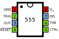
| Pin | Name | Function | Design Note |
|---|---|---|---|
| 1 | GND | Ground reference. | All voltages are measured with respect to this pin. |
| 2 | TRIG | Trigger input. | A voltage below about 1/3 VCC starts the timing interval or sets the output high. |
| 3 | OUT | Timer output. | Can drive a load within the output current and voltage limits of the selected device. |
| 4 | RESET | Active-low reset input. | Connect to VCC if reset control is not used. |
| 5 | CTRL | Control voltage input. | Often bypassed to ground with a small capacitor to reduce noise sensitivity. |
| 6 | THR | Threshold input. | When this node rises above about 2/3 VCC, the timer resets and the output goes low. |
| 7 | DIS | Discharge transistor output. | Discharges the timing capacitor during the low portion of the timing cycle. |
| 8 | VCC | Positive supply input. | Use the voltage range specified in the datasheet for the exact 555 variant. |
Astable vs Monostable Mode
| Mode | Output Behavior | Main Formula | Typical Use |
|---|---|---|---|
| Astable | Continuous rectangular waveform. | f = 1 / [0.693 × (R1 + 2R2) × C] | LED flasher, clock pulse, tone generator, simple oscillator. |
| Monostable | One pulse after each valid trigger. | T = 1.1 × R × C | One-shot delay, pulse stretching, debounce timing, trigger shaping. |
Choosing R and C Values
For best practical results, avoid values that are too extreme. Very large resistors can make the timing node sensitive to leakage current, noise, and PCB contamination. Very large electrolytic capacitors often have wide tolerance and leakage. Very small capacitors can be strongly affected by stray capacitance from wiring, breadboards, sockets, and probes.
When accurate timing is important, use stable capacitors, choose resistors with suitable tolerance, keep the timing node clean and short, and verify the circuit over temperature and supply-voltage range. For precise long delays, a microcontroller, crystal-based timer, or dedicated timing IC may be more appropriate than a basic 555 RC circuit.
Practical Accuracy Limits
| Factor | Effect on Timing |
|---|---|
| Resistor tolerance | A 5% resistor can shift the calculated time by about the same order of magnitude. |
| Capacitor tolerance | Electrolytic capacitors can vary widely from the marked value. |
| Leakage current | Leakage changes the effective charge and discharge current, especially with large resistors. |
| Supply noise | Noise on VCC or the control pin can shift trigger and threshold behavior. |
| Load current | Heavy loads can change output levels, increase heating, or require a driver transistor. |
| Device variant | Bipolar and CMOS 555 timers have different supply current, output drive, leakage, and voltage limits. |
Common Applications
| Application | Preferred Mode | Reason |
|---|---|---|
| LED flasher | Astable | Generates a repeating on-off waveform. |
| Clock pulse generator | Astable | Provides a periodic timing signal for simple digital circuits. |
| One-shot delay | Monostable | Produces one pulse with a defined width after a trigger. |
| Switch debounce | Monostable | Converts a noisy mechanical transition into a clean pulse. |
| Pulse-width modulation | Modified 555 circuit | Uses the timing network or control pin to vary pulse width. |
Common Mistakes to Avoid
| Mistake | Why It Causes Trouble |
|---|---|
| Leaving RESET floating | The output may reset unexpectedly. Tie RESET to VCC when unused. |
| Ignoring capacitor leakage | Long timing intervals can be very inaccurate with leaky capacitors. |
| Using a breadboard for high-frequency timing | Stray capacitance and inductance can distort the waveform. |
| Driving a large load directly | The 555 may overheat or the output voltage may sag. Use a transistor or MOSFET driver when needed. |
| Assuming duty cycle can reach exactly 50% in the basic astable circuit | The standard two-resistor astable circuit charges through R1 + R2 and discharges through R2, so duty cycle is normally above 50% unless modified. |
Video Reference
FAQ
Why does the 555 use 1/3 VCC and 2/3 VCC thresholds?
The classic 555 uses an internal resistor divider to create reference levels near 1/3 and 2/3 of the supply voltage. The trigger and threshold comparators use these levels to set and reset the internal latch.
Can a 555 timer make an exact 50% duty-cycle waveform?
The basic astable circuit normally produces a duty cycle above 50%. A near-50% duty cycle can be achieved with circuit modifications, such as steering charge and discharge paths with diodes or using a different oscillator arrangement.
Why is my measured timing different from the calculator?
The calculator uses ideal formulas. Real timing changes with resistor tolerance, capacitor tolerance, leakage, supply voltage, temperature, trigger shape, wiring capacitance, and the selected 555 variant.
Can I use a 555 timer for very long delays?
It is possible, but accuracy can become poor because large resistor and capacitor values are sensitive to leakage and tolerance. For reliable long delays, consider a digital timer, microcontroller, RTC, or crystal-based circuit.
Related 555 Timer Parts and Datasheets
NE555P - classic bipolar 555 timer from Texas Instruments.
NE555N - NE555 timer IC option from STMicroelectronics.
NE555PWR Datasheet - datasheet reference for a TI NE555 variant.
Related Online Calculation Tools
SMD Resistor Code Calculator - decodes 3-digit, 4-digit, and EIA-96 SMD resistor markings.
Resistor Color Code Calculator - calculates through-hole resistor values from color bands.
Capacitor Energy and Time Constant Calculator - calculates capacitor energy and RC time constants.
Ohm's Law Calculator - calculates voltage, current, resistance, and power.