Product
 Brand
Brand Articles
 Tools
Tools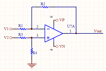

Inverting Op-Amp Resistor Calculator Overview
The Inverting Op-Amp Resistor Calculator helps determine the resistor values used in an inverting operational amplifier circuit. By entering the desired gain, selected R1 value, target output voltage, input voltage, optional offset voltage, and supply rail voltages, the calculator estimates suitable values for R2, R3, and R4.
This tool is useful when designing signal conditioning circuits, sensor interfaces, active filters, audio circuits, analog scaling stages, and bias-shift circuits where an input signal must be amplified and inverted around a defined reference point.
The calculated resistor values are given in kilo-ohms. Treat the result as a design starting point, then check the selected op-amp datasheet for output swing, input common-mode range, bandwidth, slew rate, offset voltage, input bias current, and load-drive capability.
What Is an Inverting Op-Amp?
An inverting op-amp is an operational amplifier circuit where the input signal is applied to the inverting input through an input resistor. A feedback resistor connects the output back to the same inverting input. The non-inverting input is usually connected to ground or to a reference voltage.
In a standard inverting amplifier, the output voltage changes in the opposite direction from the input voltage. This means the output is 180 degrees out of phase with the input signal. The negative sign in the gain formula represents this inversion.

What This Calculator Can Calculate
R2, the feedback resistor that sets the main inverting gain with R1.
R3, a resistor used in the reference or bias network depending on the circuit diagram.
R4, a resistor used with R3 when an offset or output bias point is required.
Whether the target output voltage is realistic for the entered positive and negative supply rails.
This calculator is specific to inverting op-amp resistor selection. For non-inverting amplifiers, differential amplifiers, instrumentation amplifiers, or active filter design, use a calculator intended for that circuit topology.
Input Parameters Explained
| Input | Meaning | Typical Unit |
|---|---|---|
| Vout | The desired output voltage or output bias point for the op-amp stage. | V |
| Gain | The target inverting gain. It is usually entered as a negative value, such as -2, -5, or -10. | V/V |
| R1 | The chosen input resistor. This value scales the rest of the resistor network. | kOhm |
| V1 | The input voltage applied to the inverting input path. | V |
| V2 | An optional reference or offset voltage. Use 0 V if no offset is required. | V |
| Vp | The positive op-amp supply rail. | V |
| Vn | The negative op-amp supply rail. In a single-supply circuit, this is often 0 V. | V |
Output Parameters Explained
| Output | Meaning |
|---|---|
| R2 | The feedback resistor paired with R1 to set the inverting gain. |
| R3 | A resistor used by the calculator's reference network. In the calculator equation, R3 is commonly set equal to R1. |
| R4 | A resistor used to establish the required offset or output bias contribution when V2 is used. |
Basic Inverting Gain Formula
For a standard inverting amplifier:

A = -R2 / R1
The output voltage is:
Vout = A * Vin
Where:
A = closed-loop voltage gain
R1 = input resistor
R2 = feedback resistor
Vin = input voltage
Vout = output voltage
Because the gain is negative, a positive input voltage produces a negative output voltage in the standard inverting configuration.
How R2 Is Calculated
If the desired gain is entered as a signed negative value, the feedback resistor can be calculated as:
R2 = -A * R1
For example, if the desired gain is -10 and R1 is 10 kOhm:
R2 = -(-10) * 10 kOhm = 100 kOhm
Some calculators describe the same relationship as:
R2 = |Gain| * R1
How R3 and R4 Are Used
In many practical op-amp circuits, extra resistors are used to provide a reference voltage, compensate for input bias current effects, or shift the output around a desired offset point. The exact purpose of R3 and R4 depends on the schematic used by the calculator.
For the common calculator model, the equations are:
R3 = R1
Vout1 = A * V1
Vout2 = Vout - Vout1
R4 = R3 * (((R1 + R2) * V2 - Vout2) / (Vout2 * R1))
R4 is meaningful only when the offset path is part of the design and the equation has valid input values. If no offset is required, V2 is normally set to 0 V, and the simplified inverting amplifier may not need the same R3/R4 network.
Example Calculation
Suppose you want an inverting amplifier with:
Gain = -5
R1 = 10 kOhm
Input voltage V1 = 0.4 V
No offset required, so V2 = 0 V
The feedback resistor is:
R2 = |Gain| * R1 = 5 * 10 kOhm = 50 kOhm
The ideal output from the inverting stage is:
Vout = -5 * 0.4 V = -2 V
If the op-amp is powered from +12 V and -12 V, this output is inside the supply range. If the same circuit is powered from a single 0 V to 5 V supply, a -2 V output cannot be produced without shifting the signal around a suitable reference voltage.
How to Use This Calculator
Choose a target inverting gain for the amplifier stage.
Select a practical R1 value based on input impedance, noise, and current requirements.
Enter the desired output voltage or output bias point.
Enter the input voltage V1.
Enter V2 only if an offset or reference voltage is required.
Enter the positive and negative supply rails as Vp and Vn.
Calculate R2, R3, and R4.
Check whether the output voltage is inside the real output swing range of the selected op-amp.
Choosing a Practical R1 Value
R1 is not only a number in the gain equation. It also affects input impedance, noise, current consumption, and bias-current error.
Lower resistor values reduce noise and bias-current error but draw more current from the signal source.
Higher resistor values reduce current draw but can increase noise and offset error.
Very high resistor values may interact with input capacitance and reduce high-frequency performance.
Very low resistor values can load the previous circuit stage and increase op-amp output current demand.
For many general-purpose op-amp circuits, resistor values in the low kOhm to hundreds of kOhm range are common, but the best choice depends on the selected op-amp and the signal source.
Output Voltage and Supply Rail Limits
The ideal formula may calculate an output voltage beyond the op-amp supply rails. A real op-amp cannot produce an output above its positive rail or below its negative rail. When the demanded output exceeds the available output swing, the signal saturates or clips.
For example, an op-amp powered from 0 V and 5 V cannot output -2 V in a standard ground-referenced circuit. A dual supply, such as +12 V and -12 V, or a shifted reference voltage may be required for signals that must swing below ground.
Even rail-to-rail op-amps usually have output swing limits that depend on load current. Always check the datasheet instead of assuming the output can reach the exact supply rails.
Inverting vs. Non-Inverting Op-Amp
| Feature | Inverting Amplifier | Non-Inverting Amplifier |
|---|---|---|
| Input connection | Input signal goes through R1 to the inverting input. | Input signal goes to the non-inverting input. |
| Phase | Output is 180 degrees out of phase with the input. | Output is in phase with the input. |
| Basic gain formula | A = -R2 / R1 | A = 1 + R2 / R1 |
| Minimum gain | Can have magnitude below, equal to, or above 1 depending on resistor ratio. | Minimum gain is 1 in the standard configuration. |
| Input impedance | Approximately set by R1. | Usually very high, depending on the op-amp input. |
Practical Design Notes
Use a gain value with the correct sign. Inverting gain is negative.
Make sure the target Vout is possible with the entered Vp and Vn supply rails.
Check the op-amp input common-mode range, especially in single-supply circuits.
Check gain-bandwidth product and slew rate if the input signal changes quickly.
Use precision resistors when gain accuracy is important.
Place supply decoupling capacitors close to the op-amp power pins in the physical circuit.
Verify the circuit in simulation or on the bench before using it in a final product.
Common Mistakes to Avoid
Entering a positive gain for an inverting amplifier when the calculator expects a negative gain.
Forgetting that the output polarity is reversed.
Choosing a target output voltage outside the op-amp supply rails.
Assuming a single-supply op-amp can output a negative voltage without a reference shift.
Using very large resistor values without considering input bias current and noise.
Ignoring gain-bandwidth product when the amplifier must work at higher frequencies.
Copying the ideal resistor result without checking available standard resistor values and tolerances.
When This Calculator Is Not Enough
This calculator is best for quick resistor selection in a simplified inverting op-amp circuit. A more detailed design process is needed for precision measurement, high-frequency amplification, low-noise circuits, large capacitive loads, high output current, single-supply operation near the rails, or circuits that require strict offset and drift control.
For those cases, check the op-amp datasheet carefully and verify the design with SPICE simulation and hardware measurements.
Frequently Asked Questions
What does this calculator output?
It outputs resistor values R2, R3, and R4 for the inverting op-amp calculator circuit. The values are given in kOhm.
Why is R2 based on the absolute value of gain?
Because the negative sign in the gain formula indicates phase inversion, not a negative resistor. The physical resistor value is positive, so R2 is calculated from the gain magnitude.
What should I enter for V2?
V2 is used when an offset or reference voltage is required. If the circuit does not need an offset, enter 0 V.
Why is my output invalid or clipped?
The requested output voltage may be outside the op-amp's supply range. Reduce the gain, reduce the input voltage, change the reference point, or use a suitable supply voltage and op-amp.
Can I use this calculator for a non-inverting amplifier?
No. This calculator is intended for inverting op-amp resistor selection. A non-inverting amplifier uses a different gain formula and resistor arrangement.
Can I use any resistor values as long as the ratio is correct?
Not always. The ratio sets the ideal gain, but the absolute resistor values affect input impedance, noise, offset error, current consumption, and bandwidth.