Discovering New and Advanced Methodology for Determining the Dynamic Characterization of Wide Bandgap Devices
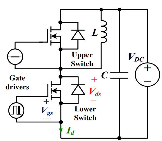
It is crucial to evaluate the dynamic characterization of different wide bandgap semiconductors and choose the most optimal option in order to increase cost-effectiveness. The double pulse test is one of the most widely used methods to evaluate the performance of power devices. The DBT provides a base for designing the converter moreover it also quantifies dynamic characteristics like dead time selection, efficiency, thermal management and switching frequency. The circuit for a basic DPT is illustrated in Figure 1, where two pulses are directed towards the test device under a clamped inductive load circuit. To capture DUT’s switching transients, the first pulse duration and DC bus voltage can be easily regulated under any current and voltage conditions.

Figure 1: A Circuit Layout of Double Pulse Test
Despite improvements in the recent measurement techniques, DBT faces issues like fast switching transients, proper current and voltage probe selections, high bandwidth requirements and alignment of voltage current parameters. On the other hand, the fast-switching characteristics of WBG devices instigate high interference in phase leg between the two devices included in the circuit, which in turn may cause high current losses.
Discovering Measurement Issues in DBT with Potential Side Effects and Learning New Ways To Overcome These Issues
Achieving accurate characterization in a double pulse test for power semiconductor devices relies on addressing various measurement challenges. The precision of timing and synchronization during pulse application is crucial to avoid result distortion due to mismatches. It is very important to control both pulse width and amplitude, with a specific focus on minimizing the impact of gate drive impedance. Monitoring and controlling temperature is another aspect that heavily manipulates measurement in DBT, moreover, it also helps in reducing the influence of parasitic elements in the test setup. Essential considerations include the proper placement and calibration of voltage and current probes, ensuring load conditions are adequate, and maintaining high-quality power supplies. Adequate signal integrity across the measurement system and the use of an advanced data acquisition system are vital for obtaining dependable and meaningful information about the switching behaviour of the devices. WBG devices are known to have high-speed switching transients which are characterized by switching waveforms of fall edges and fast rise with high fidelity. Therefore, it is of utmost importance that the probes used are of high system bandwidth of about 3 to 5 times the maximum frequency of the wave and about 10 times higher for phase calculation.
Voltage and current measurement are generally categorized by the need for high accuracy and bandwidth of probes. Voltage probes can be divided into passive probes and differential probes which have their own advantages and disadvantages, like passive probes are preferred due to their higher bandwidth and dynamic range.
It is essential to choose the correct probe as Vgs measurement on the low side in the phase leg configuration only requires probe bandwidth, however, Vgs measurement on the higher side requires galvanic isolation, CM rejection ratio, and CM voltage range in addition to probe bandwidth.
On the other hand, current measurement techniques include a current transformer, Rogowski coil, split-core current probe and coaxial shunt. Out of all these techniques coaxial shunt has the highest bandwidth and is mostly suited for measuring switching current but not switching loss, on the other hand, Rogowski has the lowest bandwidth and is not suitable for measurement. Despite these advantages, each current measurement technique introduces parasitic inductance in the power loop which ultimately affects the switching behaviour of DUT negatively. Moreover, this effect is widely seen in WBG power devices with printed circuit boards due to their fast-switching characteristics, therefore a new custom current shunt design was introduced which mitigated these parasitic effects by having several tens of 1 Ω resistors arranged in parallel.
Conclusion
Over an extensive period, silicon has traditionally been the go-to material for crafting electronic devices, prized for its affordability, moderate efficiency, and commendable performance. However, the current industry demands a better material such as WBG materials. These materials outshine silicon in crucial aspects such as efficiency, elevated junction temperatures, power density, thinner drift regions, and swifter switching speeds, positioning them as the favored materials for the future of power electronics. However, a careful evaluation of the dynamic characterization of various wide bandgap semiconductors is crucial to optimize cost-effectiveness. One widely employed method for evaluating power device performance is the double pulse test, which not only serves as a foundation for converter design but also quantifies dynamic characteristics such as dead time selection, efficiency, thermal management, and switching frequency.
The dynamic characterization of WBG devices necessitates the consideration of several key factors, for example initially, the DPT board layout should align with that of the intended converter, ensuring optimization for sensitive parasitics such as power loop inductance, common source inductance, and Miller capacitance. Secondly, probes employed for measuring switching waveforms must meet requirements for bandwidth, dynamic range, and accuracy among the latest probes, high-voltage passive probes and coaxial shunts are preferable. However, with the addition of each measuring technique, there is an increase in the parasitic inductance inside the current loop. Moreover, voltage and current probes both have their own needs and characteristics which can be manipulated in order to get the least measurement error.
 Discovering New and Advanced Methodology for Determining the Dynamic Characterization of Wide Bandgap DevicesSaumitra Jagdale15 March 20242470
For a long era, silicon has stood out as the primary material for fabricating electronic devices due to its affordability, moderate efficiency, and performance capabilities. Despite its widespread use, silicon faces several limitations that render it unsuitable for applications involving high power and elevated temperatures. As technological advancements continue and the industry demands enhanced efficiency from devices, these limitations become increasingly vivid. In the quest for electronic devices that are more potent, efficient, and compact, wide bandgap materials are emerging as a dominant player. Their superiority over silicon in crucial aspects such as efficiency, higher junction temperatures, power density, thinner drift regions, and faster switching speeds positions them as the preferred materials for the future of power electronics.
Read More A Comprehensive Guide to FPGA Development BoardsUTMEL11 September 202514674
This comprehensive guide will take you on a journey through the fascinating world of FPGA development boards. We’ll explore what they are, how they differ from microcontrollers, and most importantly, how to choose the perfect board for your needs. Whether you’re a seasoned engineer or a curious hobbyist, prepare to unlock new possibilities in hardware design and accelerate your projects. We’ll cover everything from budget-friendly options to specialized boards for image processing, delve into popular learning paths, and even provide insights into essential software like Vivado. By the end of this article, you’ll have a clear roadmap to navigate the FPGA landscape and make informed decisions for your next groundbreaking endeavor.
Read More Applications of FPGAs in Artificial Intelligence: A Comprehensive GuideUTMEL29 August 20253606
This comprehensive guide explores FPGAs as powerful AI accelerators that offer distinct advantages over traditional GPUs and CPUs. FPGAs provide reconfigurable hardware that can be customized for specific AI workloads, delivering superior energy efficiency, ultra-low latency, and deterministic performance—particularly valuable for edge AI applications. While GPUs excel at parallel processing for training, FPGAs shine in inference tasks through their adaptability and power optimization. The document covers practical implementation challenges, including development complexity and resource constraints, while highlighting solutions like High-Level Synthesis tools and vendor-specific AI development suites from Intel and AMD/Xilinx. Real-world applications span telecommunications, healthcare, autonomous vehicles, and financial services, demonstrating FPGAs' versatility in mission-critical systems requiring real-time processing and minimal power consumption.
Read More 800G Optical Transceivers: The Guide for AI Data CentersUTMEL24 December 20253830
The complete guide to 800G Optical Transceiver standards (QSFP-DD vs. OSFP). Overcome supply shortages and scale your AI data center with Utmel Electronic.
Read More Xilinx FPGAs: From Getting Started to Advanced Application DevelopmentUTMEL09 September 20254299
This guide is your comprehensive roadmap to understanding and mastering the world of Xilinx FPGA technology. From selecting your first board to deploying advanced AI applications, we'll cover everything you need to know to unlock the potential of these remarkable devices. The global FPGA market is on a significant growth trajectory, expected to expand from USD 8.37 billion in 2025 to USD 17.53 billion by 2035. This surge is fueled by the relentless demand for high-performance, adaptable computing in everything from 5G networks and data centers to autonomous vehicles and the Internet of Things (IoT). This guide will walk you through the key concepts, tools, and products in the Xilinx ecosystem, ensuring you're well-equipped to be a part of this technological revolution.
Read More
Subscribe to Utmel !
![AT88SC25616C-PU]() AT88SC25616C-PU
AT88SC25616C-PUMicrochip Technology
![FM3164-G]() FM3164-G
FM3164-GCypress Semiconductor Corp
![HCS301-I/P]() HCS301-I/P
HCS301-I/PMicrochip Technology
![L9660TR]() L9660TR
L9660TRSTMicroelectronics
![MOC3062VM]() MOC3062VM
MOC3062VMON Semiconductor
![MOC3020SR2M]() MOC3020SR2M
MOC3020SR2MON Semiconductor
![FGBS3040E1-F085]() FGBS3040E1-F085
FGBS3040E1-F085ON Semiconductor
![ATSHA204-TSU-T]() ATSHA204-TSU-T
ATSHA204-TSU-TMicrochip Technology
![AD8196ACPZ]() AD8196ACPZ
AD8196ACPZAnalog Devices Inc.
![TLE8110EDXUMA1]() TLE8110EDXUMA1
TLE8110EDXUMA1Infineon Technologies


 Product
 Brand
Brand Articles
 Tools
Tools


