
 Product
 Brand
Brand Articles
 Tools
Tools
Introduction to BGA Package
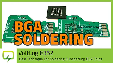
Best Technique For Soldering & Inspecting BGA Chips
Catalog |
Ⅰ What is BGA package?
LSI, VLSI, and ULSI emerged one after another in the 1990s with advances in integration technology, improvements in equipment, and the use of deep submicron technology. Silicon single-chip integration continues to increase, the requirements for integrated circuit packaging become more stringent, the number of I/O pins increases sharply, and power consumption increases. To meet the needs of development, on the basis of the original package varieties, a new variety was added - BGA Package (Ball Grid Array Package).
The I/O terminals of the BGA package are distributed under the package in an array of circular or columnar solder joints. The memory packaged with BGA technology can increase the memory capacity by two to three times without changing the size of the memory. Compared with TSOP, BGA has a smaller volume, better heat dissipation performance, and electrical performance. BGA package technology has greatly improved the storage capacity per square inch. Memory products using BGA packaging technology have only one-third of the volume of the TSOP package under the same capacity. In addition, compared with the traditional TSOP packaging method, the BGA package is a faster and more effective way to dissipate heat.
Ⅱ BGA package features
As soon as BGA appeared, it became the best choice for high-density, high-performance, multi-function, and high-I/O pin packaging for VLSI chips such as CPUs and north-south bridges.
Its characteristics are:
1. Although the number of I/O pins has increased, the pin spacing is much larger than QFP, which improves the assembly yield;
2. Although its power consumption is increased, BGA can be welded by the controllable collapse chip method, referred to as C4 welding, which can improve its electric heating performance;
3. Compared with QFP, the thickness is reduced by more than 1/2, and the weight is reduced by more than 3/4;
4. The parasitic parameters are reduced, the signal transmission delay is small, and the frequency of use is greatly improved;
5. Coplanar welding can be used for assembly, with high reliability;
6. BGA package is still the same as QFP and PGA, occupying too much substrate area;
Intel Corporation has a high level of integration (more than 3 million transistors in a single chip) and high power consumption CPU chips, such as Pentium, Pentium Pro, Pentium Ⅱ, using ceramic pin grid array packaging CPGA and ceramic ball grid array packaging CBGA, and install a miniature exhaust fan on the shell to dissipate heat, so as to achieve the stable and reliable operation of the circuit.
Ⅲ BGA package classification
There are many types of BGA packages, which can be divided into peripheral type, staggered type,
PBGA package 1 and full array type according to the arrangement of solder balls.
According to the different substrates, it is mainly divided into PBGA (Plastic BGA), CBGA (Ceramic BGA), FCBGA (Filpchip BGA), TBGA (Tape BGA).
PBGA package
PBGA is the most commonly used form of the BGA package, which is made of plastic materials and plastic processes. The type of substrate used is PCB substrate material (BT resin/glass laminate). After the bare chip is connected to the top of the substrate and the lead frame by bonding and WB technology, the overall plastic is achieved by injection molding (epoxy film-plastic mixture). In Intel series CPU, Pentium II, III, IV processors all adopt this kind of packaging form.

PBGA package 1
The solder ball material is a low-melting eutectic solder alloy 63Sn37Pb with a diameter of about 1mm and a pitch range of 1.27-2.54mm. The connection between the solder ball and the bottom of the package does not require additional solder. When assembling, the solder balls melt and join with the solder plate on the PCB surface, showing a barrel shape.

PBGA package 2
The characteristics of PBGA package are mainly manifested in the following four aspects:
1. Low production cost and high-cost performance.
2. The solder balls participate in the formation of reflow solder joints.
3. Good thermal matching with epoxy resin substrate, high quality and good performance when assembled to PCB.
4. Sensitive to moisture, PoPCorn effect is serious, and the QFP package height is also a technical challenge.
CBGA package
CBGA is formed by mounting the bare chip on the top surface of the ceramic multilayer substrate carrier. The metal cover is soldered on the substrate with sealing solder to protect the chip, leads, and pads. The connected package is airtight. Pentium I, II, and Pentium Pro processors have all used this package.

CBGA package 1
CBGA uses a multilayer ceramic wiring substrate. The solder ball material is a high melting point 90Pb10Sn eutectic solder. The connection between the solder ball and the package body uses low-temperature eutectic solder 63Sn37Pb, and it adopts a cover + glass air seal, which belongs to the category of airtight packaging.

CBGA package 2
The characteristics of the CBGA package are mainly manifested in the following six aspects:
1. Insensitive to moisture, good reliability, excellent electrical and thermal performance.
2. Good matching with ceramic substrate CTE.
3. The reworkability of connecting chips and components are better.
4. The bare chip adopts FCB technology, and the interconnection density is higher.
5. Higher packaging cost.
6. Poor CTE matching with epoxy resin and other substrates.
FCBGA package
FCBGA is currently the most important packaging format for graphics acceleration chips. This packaging technology began in the 1960s. At that time, IBM developed the so-called C4 (Controlled Collapse Chip Connection) technology for the assembly of large computers. It was then further developed to the point where the surface tension of the molten bumps could be used to support the weight of the chip and control the height of the bumps, and became the direction of development for flip-chip technology.
This package uses small balls instead of pins to connect to the processor. A total of 479 balls are required, and the diameters are all 0.78 mm, which can provide the shortest external connection distance. FCBGA is interconnected with the substrate through FCB technology. The difference from PBGA is that the bare chip faces down.

FCBGA package
The characteristics of FCBGA packaging are mainly manifested in the following three aspects:
1. Excellent electrical performance, while reducing the loss and inductance between component interconnections, reducing electromagnetic interference problems, and withstanding higher frequencies.
2. Increase the density of I/O, improve the efficiency of use, and effectively reduce the area of the substrate by 30% to 60%.
3. Good heat dissipation, which can improve the stability of the chip during high-speed operation.
TBGA package
TBGA, also known as automatic array carrier tape bonding, is a relatively novel form of the BGA package. The type of substrate used is a PI multilayer wiring substrate, the solder ball material is a high melting point solder alloy, and a low melting point solder alloy is used for soldering.

TBGA package
The characteristics of TBGA packaging are mainly manifested in the following five aspects:
1. Good thermal matching with epoxy resin PCB substrate.
2. The thinnest BGA package form is conducive to chip thinning.
3. Compared with CBGA, the cost is lower.
4. Sensitive to heat and humidity.
5. The chip is light and small, and the self-calibration deviation is large compared with other BGA types.
Ⅳ Process flow
The substrate or intermediate layer is a very important part of the BGA package. In addition, to interconnect wiring, it can also be used for impedance control and for inductance/resistance/capacitance integration. Therefore, the substrate material is required to have a high glass transition temperature rS (approximately 175~230°C), high dimensional stability and low moisture absorption, as well as good electrical properties and high reliability. The metal film, the insulating layer and the substrate medium should also have higher adhesion properties.
1. PBGA packaging process
① Preparation of PBGA substrate
Laminate extremely thin (12~18μm thick) copper foil on both sides of the BT resin/glass core board, and then perform drilling and through-hole metallization. Use conventional PCB plus 3232 technology to make patterns on both sides of the substrate, such as conduction strips, electrodes, and an array of pads for mounting solder balls. Then add a solder mask and make a pattern, exposing the electrode and solder area. In order to improve production efficiency, a substrate usually contains multiple PBG substrates.
② Packaging process
Wafer thinning→wafer cutting→chip bonding→plasma cleaning→wire bonding→plasma cleaning→molded packaging→assembly of solder balls→reflow soldering→surface marking→separation→final inspection→test hopper packaging
The chip is bonded to the substrate with a silver-filled epoxy adhesive. Then gold wire bonding is used to achieve the connection between the chip and the substrate. Then molded plastic package or liquid adhesive potting is used to protect the chip, solder line and pad. A specially designed pick-up tool is used to place the solder balls 62/36/2Sn/Pb/Ag or 63/37/Sn/Pb with a melting point of 183°C and a diameter of 30 mil (0.75 mm) on the pads and reflow them in a conventional reflow oven, with a maximum processing temperature of no more than 230°C. Next, the substrate is centrifugally cleaned with CFC inorganic cleaner to remove solder and fiber particles left on the package. This is followed by marking, separation, final inspection, testing, and packaging for storage. The above is the process of lead bonding PBGA packaging.
2. FC-CBGA packaging process
① Ceramic substrate
The substrate of FC-CBGA is a multilayer ceramic substrate, and its production is quite difficult. Because the wiring density of the substrate is high, the pitch is narrow, there are many through holes, and the coplanarity of the substrate is relatively high.
Its main process is: first co-fire the multilayer ceramic sheet into a multilayer ceramic metalized substrate at a high temperature, then make multilayer metal wiring on the substrate, and then electroplating. In the assembly of CBGA, the CTE mismatch between the substrate, the chip, and the PCB is the main factor causing the failure of CBGA products. To improve this situation, in addition to the CCGA structure, another ceramic substrate-HITCE ceramic substrate can also be used.
②Packaging process
Preparation of wafer bumps -> wafer dicing -> chip flip and reflow soldering -> underfill thermal grease, distribution of sealing solder -> capping -> assembly solder ball -> reflow soldering -> marking -> separation ->Final inspection->Test->Packing
3. TBGA packaging process
① TBGA tape
The carrier tape of TBGA is usually made of polyimide material.
During fabrication, both sides of the carrier tape are first copper coated, then nickel and gold plated. Next, through-hole punching, through-hole metallization, and graphics are produced. In this lead bonded TBGA, the encapsulated heat sink is a solid addition to the package and the core cavity substrate of the shell, so the carrier tape is bonded to the heat sink using a pressure-sensitive bonding agent before encapsulation.
②Packaging process
Wafer thinning→wafer cutting→chip bonding→cleaning→wire bonding→plasma cleaning→liquid sealant potting→assembly of solder balls→reflow soldering→surface marking→separation→final inspection→testing→packaging
 UTMEL
UTMEL
We are the professional distributor of electronic components, providing a large variety of products to save you a lot of time, effort, and cost with our efficient self-customized service. careful order preparation fast delivery service
1.What is a BGA package?
B. G. (Ball Grid Array) A popular surface mount chip package that uses a grid of solder balls as its connectors. Available in plastic and ceramic varieties, BGA is noted for its compact size, high lead count, and low inductance, which allows lower voltages to be used.
2.What is BGA testing?
Ball Grid Array (BGA) devices differ from normally-packaged devices in that all of their external connections are made through balls of solder between the bottom face of the device and the circuit board rather than through pins protruding from the side of the device.
 Discovering New and Advanced Methodology for Determining the Dynamic Characterization of Wide Bandgap DevicesSaumitra Jagdale15 March 20242612
For a long era, silicon has stood out as the primary material for fabricating electronic devices due to its affordability, moderate efficiency, and performance capabilities. Despite its widespread use, silicon faces several limitations that render it unsuitable for applications involving high power and elevated temperatures. As technological advancements continue and the industry demands enhanced efficiency from devices, these limitations become increasingly vivid. In the quest for electronic devices that are more potent, efficient, and compact, wide bandgap materials are emerging as a dominant player. Their superiority over silicon in crucial aspects such as efficiency, higher junction temperatures, power density, thinner drift regions, and faster switching speeds positions them as the preferred materials for the future of power electronics.
Read More A Comprehensive Guide to FPGA Development BoardsUTMEL11 September 202519863
This comprehensive guide will take you on a journey through the fascinating world of FPGA development boards. We’ll explore what they are, how they differ from microcontrollers, and most importantly, how to choose the perfect board for your needs. Whether you’re a seasoned engineer or a curious hobbyist, prepare to unlock new possibilities in hardware design and accelerate your projects. We’ll cover everything from budget-friendly options to specialized boards for image processing, delve into popular learning paths, and even provide insights into essential software like Vivado. By the end of this article, you’ll have a clear roadmap to navigate the FPGA landscape and make informed decisions for your next groundbreaking endeavor.
Read More 800G Optical Transceivers: The Guide for AI Data CentersUTMEL24 December 20259771
The complete guide to 800G Optical Transceiver standards (QSFP-DD vs. OSFP). Overcome supply shortages and scale your AI data center with Utmel Electronic.
Read More The 2026 Engineer’s Guide: Choosing the Right MCU for Your Next IoT & New Energy ProjectUTMEL30 April 2026647
A comprehensive comparison of 2026's leading MCUs from ST, NXP, and Microchip across power efficiency, processing performance, connectivity, and ecosystems to help engineers select the optimal chip for next-gen IoT and new energy projects.
Read More AI Server Components: Engineering Next-Gen Data Center Hardware for 100kW RacksUTMEL15 May 2026361
The transition from traditional enterprise IT to AI-driven workloads has rendered legacy data center hardware obsolete, forcing infrastructure planners to re-engineer server components for extreme thermal environments.
Read More
Subscribe to Utmel !
![HCS500T/SM]() HCS500T/SM
HCS500T/SMMicrochip Technology
![AT88SC1616C-SH]() AT88SC1616C-SH
AT88SC1616C-SHMicrochip Technology
![EL3022]() EL3022
EL3022Everlight Electronics Co Ltd
![FOD4108V]() FOD4108V
FOD4108VON Semiconductor
![HCS410/ST]() HCS410/ST
HCS410/STMicrochip Technology
![ATECC108-SSHCZ-T]() ATECC108-SSHCZ-T
ATECC108-SSHCZ-TMicrochip Technology
![ATECC108-SSHDA-T]() ATECC108-SSHDA-T
ATECC108-SSHDA-TMicrochip Technology
![MOC3081VM]() MOC3081VM
MOC3081VMON Semiconductor
![MCP2036T-I/MG]() MCP2036T-I/MG
MCP2036T-I/MGMicrochip Technology
![ATSHA204A-MAHCZ-S]() ATSHA204A-MAHCZ-S
ATSHA204A-MAHCZ-SMicrochip Technology


