What is the Difference between an Integrated Circuit and a Chip

What Is An Integrated Circuit (IC)
Executive Summary: IC vs. Chip (2026 Update)
The Core Difference: While often used interchangeably, strictly speaking, an Integrated Circuit (IC) refers to the internal silicon wafer containing microscopic circuits, whereas a Chip refers to the final packaged product (the black square with pins) that protects the IC and connects it to a device.
2026 Snapshot: Modern AI chips now utilize 2nm process nodes and 3D stacking technology, packing billions of transistors into a space smaller than a fingernail to power Generative AI and IoT devices.
| Quick Navigation: |
| Ⅰ. What is an Integrated Circuit (IC)? |
| Ⅱ. What is a "Chip" in electronics? |
| Ⅲ. Key Differences: Manufacturing & Function |
Direct Answer: An integrated circuit (IC) is the microscopic set of electronic circuits on a semiconductor plate, while a "chip" is the packaged, usable component found in your devices.
According to Jack Kilby, the Nobel Prize winner who created the first hybrid IC, an integrated circuit is a semiconductor piece in which every element of an electronic circuit is completely integrated. In the context of 2026 technology, an IC is an ultra-sophisticated electronic circuit made by dispersing a pattern of trace elements onto a semiconductor substrate (typically silicon or gallium nitride).
The development of integrated circuit technology starting in 1958 initiated a global digital transformation. By 2026, this technology has evolved from simple logic gates to neural processing units (NPUs) capable of quadrillions of operations per second.
Ⅰ. What is an Integrated Circuit (IC) in 2026?
An integrated circuit (IC) is a microscopic array of electronic components (transistors, resistors, capacitors) fabricated on a single wafer of semiconductor material.
It functions as the "brain" or "memory" of modern electronics. By consolidating components into a singular microstructure, ICs have enabled the shift toward miniaturization, extreme power efficiency, and artificial intelligence.
Key characteristics of modern ICs include:
Composition: Transistors and wirings are photolithographically printed on semiconductor wafers.
Materials: While Silicon (Si) remains dominant, 2026 sees increased use of Silicon Carbide (SiC) and Gallium Nitride (GaN) for power efficiency.
Identification: In circuit diagrams, they are denoted by the prefix "U" or "IC."
Historically, Jack Kilby and Robert Noyce created the first ICs based on germanium and silicon. Today, the industry has moved to "Chiplet" architecture, where multiple smaller ICs are stitched together to form powerful processors for data centers and electric vehicles.
Ⅱ. What is a "Chip" in practical terms?
A "chip" is the colloquial industry term for the final, packaged semiconductor product that is mounted onto a circuit board.
While technical engineers distinguish between the "die" (the internal crystal) and the "chip" (the package), the general public and supply chain use the term "chip" to cover the entire unit. It serves as the physical carrier for the integrated circuit.
In 2026, chips are ubiquitous, found in everything from smart toasters to autonomous vehicles. A single high-end AI chip today may contain over 100 billion transistors, a stark contrast to the handful of components in early microchips.
Ⅲ. IC vs. Chip: Key Technical Differences
1. Evolution of Capability (Moore's Law 2.0)
The primary differentiator is functional density. Early transistors were discrete and bulky. The IC unified these into a single unit.
In 2026, the industry follows "Moore's Law 2.0" or "More than Moore." While the physical shrinking of transistors is approaching atomic limits (Angstrom era), capacity is now increased through 3D stacking (High Bandwidth Memory) and advanced packaging. This allows modern chips to handle complex Generative AI workloads locally on devices, reducing the need for cloud processing.
2. Packaging and Form Factor
The "Chip" is the vessel; the "IC" is the cargo. Chips are the method of miniaturizing circuits and protecting them for assembly.
Common Package Types in 2026:
DIP (Dual In-Line Package): The legacy rectangular standard with parallel rows of pins (2.54mm spacing), still used in hobbyist electronics.
BGA (Ball Grid Array): Used for high-performance processors (CPUs/GPUs), utilizing solder balls beneath the chip for high-density connections.
SiP (System in Package): A modern standard where multiple ICs (memory, processor, radio) are bundled into a single chip body.
The IC packaging is critical. It bridges the microscopic nanometer-scale wiring of the internal die to the millimeter-scale wiring of the Printed Circuit Board (PCB).
3. Manufacturing Complexity
The creation of an IC differs from the assembly of a Chip:
Front-End (IC Fabrication): This occurs in a cleanroom. It involves Extreme Ultraviolet (EUV) lithography to print circuits onto a silicon wafer. This process creates the Integrated Circuit.
Back-End (Chip Packaging): The wafer is cut into individual dies. These dies are then mounted, wire-bonded (or flip-chipped), and encapsulated in epoxy or ceramic. This creates the Chip.
Prior to the development of integrated circuits, engineers used vacuum tubes—bulky, hot, and unreliable components. Today's integrated chips allow for circuit components to be microscopic, enabling the existence of smartphones, wearables, and advanced medical implants.
1. What does the chip do?
The role of the chip: It can control everything from computers to mobile phones to digital microwave ovens. Although the cost of designing and developing a complex integrated circuit is very high, the cost per integrated circuit is minimized when distributed over products, often in the millions. The performance of integrated circuits is high because the small size brings short paths, enabling low-power logic circuits to be applied at fast switching speeds.
2. Are chips the same as integrated circuits?
Different.
Chip is a general term for semiconductor component products. It is the carrier of integrated circuits, which is divided into wafers.
Chip is an abbreviation of integrated circuit. In fact, the real meaning of the word chip refers to a little large semiconductor chip inside the integrated circuit package, that is, the die. Strictly speaking, chips and integrated circuits are not interchangeable.
Integrated circuits are manufactured through semiconductor technology, thin-film technology and thick-film technology. Any circuit that miniaturizes a certain function and is made in a certain packaged circuit form can be called an integrated circuit.
3. What does a chip have to do with an integrated circuit?
The previous circuits of the chip were all circuits that were connected together by discrete components. After the transistor was invented, the integrated circuit was invented in 1961. This is a revolution in circuit design. It connects the various elements of the entire transistor circuit, and makes it on a semiconductor substrate at the same time, forming an inseparable whole, breaking the concept of the original circuit, breaking the original design method of discrete components, and realizing the The "brain" of a computer and all electronic devices, which is a combination of materials, components, and circuits, is called a microprocessor, or chip.
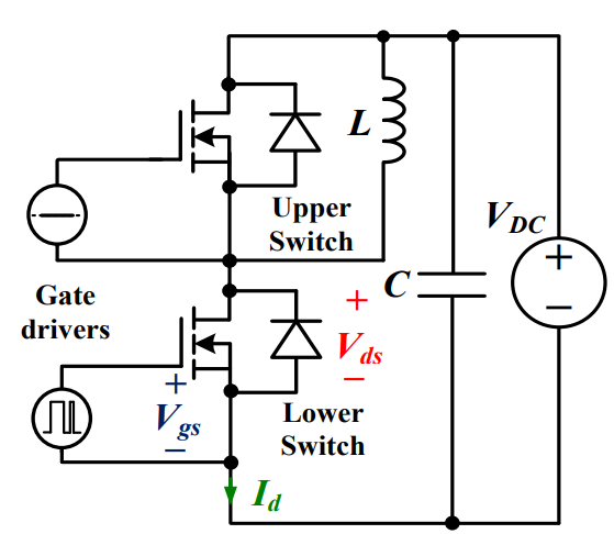 Discovering New and Advanced Methodology for Determining the Dynamic Characterization of Wide Bandgap DevicesSaumitra Jagdale15 March 20242507
For a long era, silicon has stood out as the primary material for fabricating electronic devices due to its affordability, moderate efficiency, and performance capabilities. Despite its widespread use, silicon faces several limitations that render it unsuitable for applications involving high power and elevated temperatures. As technological advancements continue and the industry demands enhanced efficiency from devices, these limitations become increasingly vivid. In the quest for electronic devices that are more potent, efficient, and compact, wide bandgap materials are emerging as a dominant player. Their superiority over silicon in crucial aspects such as efficiency, higher junction temperatures, power density, thinner drift regions, and faster switching speeds positions them as the preferred materials for the future of power electronics.
Read More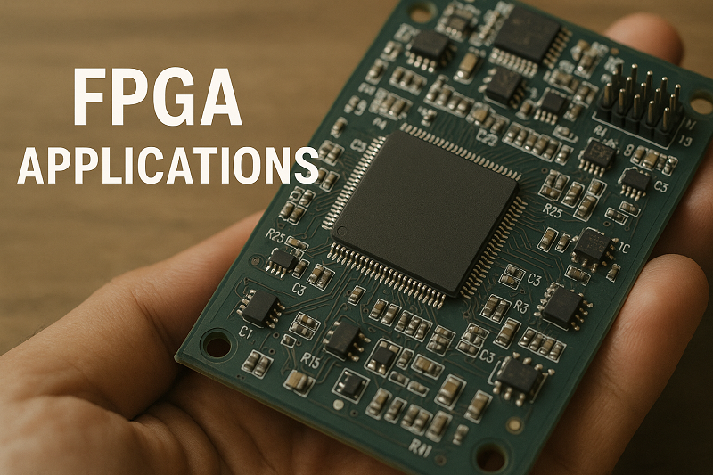 A Comprehensive Guide to FPGA Development BoardsUTMEL11 September 202515956
This comprehensive guide will take you on a journey through the fascinating world of FPGA development boards. We’ll explore what they are, how they differ from microcontrollers, and most importantly, how to choose the perfect board for your needs. Whether you’re a seasoned engineer or a curious hobbyist, prepare to unlock new possibilities in hardware design and accelerate your projects. We’ll cover everything from budget-friendly options to specialized boards for image processing, delve into popular learning paths, and even provide insights into essential software like Vivado. By the end of this article, you’ll have a clear roadmap to navigate the FPGA landscape and make informed decisions for your next groundbreaking endeavor.
Read More Applications of FPGAs in Artificial Intelligence: A Comprehensive GuideUTMEL29 August 20253880
This comprehensive guide explores FPGAs as powerful AI accelerators that offer distinct advantages over traditional GPUs and CPUs. FPGAs provide reconfigurable hardware that can be customized for specific AI workloads, delivering superior energy efficiency, ultra-low latency, and deterministic performance—particularly valuable for edge AI applications. While GPUs excel at parallel processing for training, FPGAs shine in inference tasks through their adaptability and power optimization. The document covers practical implementation challenges, including development complexity and resource constraints, while highlighting solutions like High-Level Synthesis tools and vendor-specific AI development suites from Intel and AMD/Xilinx. Real-world applications span telecommunications, healthcare, autonomous vehicles, and financial services, demonstrating FPGAs' versatility in mission-critical systems requiring real-time processing and minimal power consumption.
Read More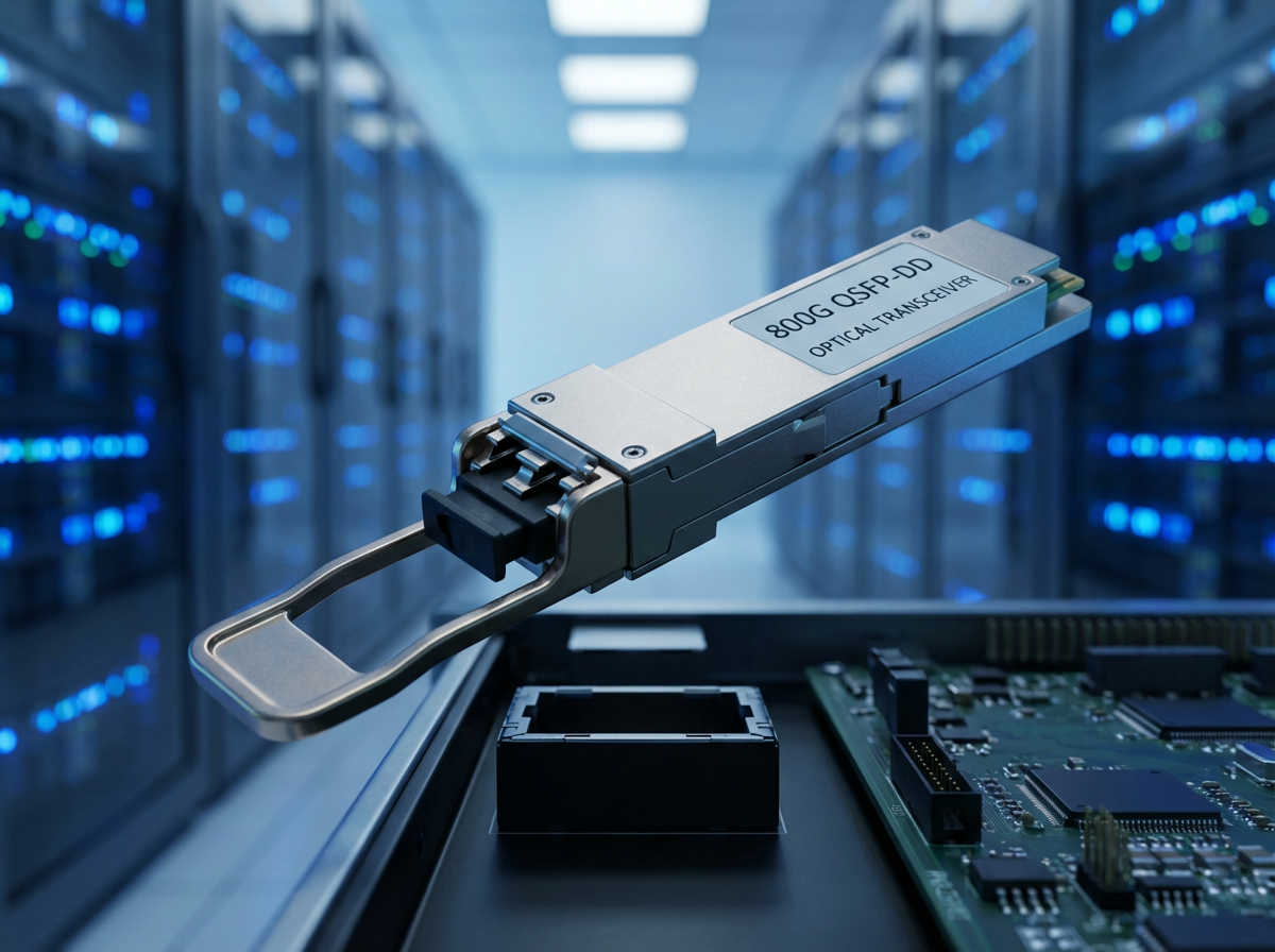 800G Optical Transceivers: The Guide for AI Data CentersUTMEL24 December 20254725
The complete guide to 800G Optical Transceiver standards (QSFP-DD vs. OSFP). Overcome supply shortages and scale your AI data center with Utmel Electronic.
Read More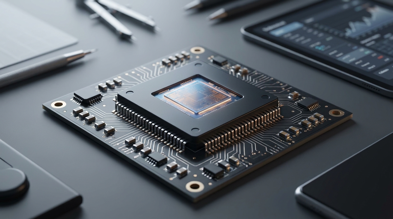 The 2026 Engineer’s Guide: Choosing the Right MCU for Your Next IoT & New Energy ProjectUTMEL30 April 202668
A comprehensive comparison of 2026's leading MCUs from ST, NXP, and Microchip across power efficiency, processing performance, connectivity, and ecosystems to help engineers select the optimal chip for next-gen IoT and new energy projects.
Read More
Subscribe to Utmel !
![FOD3180SDV]() FOD3180SDV
FOD3180SDVON Semiconductor
![ADUM4135BRWZ]() ADUM4135BRWZ
ADUM4135BRWZAnalog Devices Inc.
![ISO5452DWR]() ISO5452DWR
ISO5452DWRTexas Instruments
![ISO5452DW]() ISO5452DW
ISO5452DWTexas Instruments
![ATECC608A-SSHDA-T]() ATECC608A-SSHDA-T
ATECC608A-SSHDA-TMicrochip Technology
![HCS500-I/SM]() HCS500-I/SM
HCS500-I/SMMicrochip Technology
![AT88SC0404CA-SH]() AT88SC0404CA-SH
AT88SC0404CA-SHMicrochip Technology
![FSSD06BQX]() FSSD06BQX
FSSD06BQXON Semiconductor
![HCNW3120-500E]() HCNW3120-500E
HCNW3120-500EBroadcom Limited
![FOD8342TR2]() FOD8342TR2
FOD8342TR2ON Semiconductor


 Product
 Brand
Brand Articles
 Tools
Tools


