Comprehensive Analysis of Each Functional Circuit of Switching Power Supply
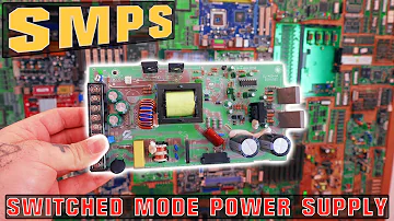
How SMPS works | What Components We Need? Switched Mode Power Supply
1. Circuit composition of switching power supply
An input electromagnetic interference filter (EMI), a rectifier filter circuit , a power conversion circuit, a PWM controller circuit , and an output rectifier filter circuit make up the switching power supply's primary circuit. Input over-voltage and under-voltage protection circuits, output over-voltage and under-voltage protection circuits, output over-current protection circuits, and output short-circuit protection circuits are all included in the auxiliary circuits.
2. The principle and common circuit of input circuit
(1)Principle of AC input rectifier filter circuit:

Figure. 1
①Lightning protection circuit: When lightning strikes, high voltage is generated and imported into the power supply via the power grid, a circuit made up of MOV1, MOV2, MOV3: F1, F2, F3, and FDG1 is utilized to protect the power supply. When the voltage connected to both ends of the varistor exceeds its working voltage, its resistance value drops, causing the varistor to consume high-voltage energy. F1, F2, and F3 will burn if the current is too high, protecting the subsequent circuit.
②The double-type filter network consists of C1, L1, C2, and C3 suppresses the electromagnetic noise and clutter signal of the input power supply prevents interference, and also inhibits high-frequency clutter generated by the power supply. There is grid interference. It is important to charge C5 when the power is turned on. The addition of an RT1 (thermistor) can effectively avoid inrush current due to the excessive instantaneous current. Because the RT1 resistor uses all of the instantaneous energy, the resistance value of RT1 falls once the temperature rises after a specific amount of time (RT1 is a negative temperature coefficient element), and the succeeding circuit may function normally.
③ Rectifier and filter circuit : After BRG1 rectifies the AC voltage, C5 filters it to provide a relatively pure DC voltage. The output AC ripple will rise as the capacity of C5 decreases.
(2) Principle of DC input filter circuit:

Figure. 2
①The double-type filter network consists of C1, L1, and C2 suppresses the electromagnetic noise and clutter signal of the input power supply, prevents interference to the power supply, and also prevents high-frequency clutter created by the power supply from damaging the power grid. L2 and L3 are differential mode inductors, whereas C3 and C4 are safety capacitors.
②An anti-surge circuit is formed by R1, R2, R3, Z1, C6, Q1, Z2, R4, R5, Q2, RT1, and C7. Due to the presence of C6, Q2 does not conduct at the start, and the current forms a loop through RT1. Q2 is turned on when the voltage on C6 reaches the controlled value of Z1. If C8 is leaking or the circuit of the latter stage is short-circuited, the voltage drop created by the current on RT1 increases at startup, Q1 is switched on, and Q2 is not turned on, RT1 will be burned in a very short time. The back-end circuit must be protected.
3. Power conversion circuit
(1) The working principle of MOS tube:
The MOSFET (MOS tube), which works by harnessing the electroacoustic effect on the surface of the semiconductor, is now the most extensively used insulated gate field effect transistor. Surface field effect devices are another name for them. The input resistance can be increased to 105 ohms because the gate is in a non-conductive state. The gate-source voltage is used by the MOS tube to control the drain current by changing the amount of charge induced on the semiconductor's surface.
(2) Common schematic diagram:
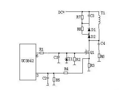
Figure. 3
(3) Working principle:
R4, C3, R5, R6, C4, D1, and D2 form a buffer that is connected in parallel with the switch MOS tube, reducing the switch tube's voltage stress, EMI, and preventing secondary breakdown. The primary coil of the transformer is prone to create peak voltage and peak current when the switch tube Q1 is turned off. These components work together to effectively absorb peak voltage and current. The current peak signal measured from R3 is used to govern the duty cycle of the current working cycle, hence it is the current working cycle's current limit.
The UC3842 ceases operating when the voltage on R5 exceeds 1V, and the switch tube Q1 is turned off immediately. The junction capacitors CGS and CGD in R1 and Q1 create an RC network, and the capacitor's charging and discharging directly impact the switch's switching speed. If R1 is too tiny, oscillation is simple to produce, and electromagnetic interference is high; if R1 is too large, the switch tube's switching speed is reduced. Z1 normally keeps the MOS tube's GS voltage below 18V, thereby protecting it.Q1's gate regulated voltage is formed like a saw. When the duty cycle of Q1 is higher, the conduction time of Q1 is longer, and the energy stored by the transformer is higher; when Q1 is turned off, the transformer passes through D1, D2, R5, R4, and C3 to release energy and reset the magnetic field, preparing the transformer for the next energy storage and transfer. The IC adjusts the duty cycle of the 6 pin saw-shaped wave based on the output voltage and current, effectively stabilizing the machine's output current and voltage. The peak voltage absorption circuits are C4 and R6.
(4) Push-pull power conversion circuit:
Q1 and Q2 will be turned on in turn.
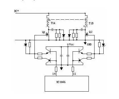
Figure. 4
(5) Power conversion circuit with drive transformer:
T2 is the drive transformer, T1 is the switching transformer, and TR1 is the current loop.
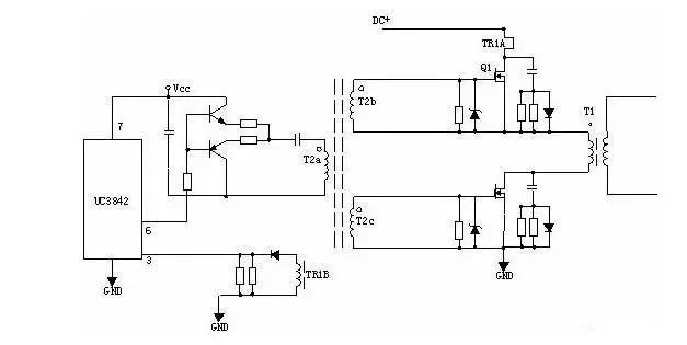
Figure. 5
4. Output rectifier filter circuit
(1) Forward rectifier circuit:
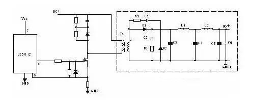
Figure. 6
The primary and secondary phases of the T1 switching transformer are in phase. R1, C1, R2, and C2 are peak clipping circuits, whereas D1 is a rectifier diode and D2 is a freewheeling diode. C4, L2, and C5 comprise a -type filter and L1 is a freewheeling inductor.
(2) Flyback rectifier circuit:

Figure. 7
T1 is a switching transformer with opposite-phase primary and secondary phases. R1 and C1 are peak clipping circuits, and D1 is a rectifier diode. A freewheeling inductor is L1, a dummy load is R2, and a -type filter is formed by C4, L2, and C5.
(3) Synchronous rectifier circuit:
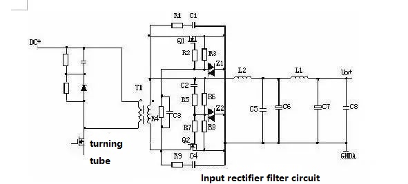
Figure. 8
Working principle: When the transformer secondary is positive, current flows through C2, R5, R6, R7, causing Q2 to conduct, the circuit to create a loop, and Q2 to function as a rectifier tube. Because Q1 is reverse biased, its gate is turned off. When the transformer secondary's lower end is positive, current flows via C3, R4, and R2 to cause Q1 to conduct, and Q1 becomes a freewheeling tube. Because Q2 is reverse biased, its gate is turned off. C6, L1, and C7 form a -type filter and L2 is a freewheeling inductor. Peak clipping circuits are R1, C1, R9, and C4.
5. Principle of Voltage Regulator Loop
(1) Schematic diagram of the feedback circuit:
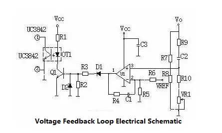
Figure. 9
(2) Working principle:
The voltage of the U1 3 pin rises when the output U0 rises, after the sampling resistors R7, R8, R10, VR1 divide the voltage, and when it surpasses the U1 2 pin reference voltage, the U1 1 pin outputs a high level, turning on Q1 and causing the optocoupler OT1 to emit light. When the diode generates light, the phototransistor turns on, and the potential of the UC3842 pin 1 drops, the output duty ratio of the U1 6 pin changes, and the U0 decreases. The voltage of pin U13 decreases as the output U0 decreases. When the potential of the UC38421 pin falls below the reference voltage of pin U12, pin U11 outputs a low level, Q1 does not conduct, the optocoupler OT1 LED does not emit light, the phototransistor does not conduct, and the potential of the UC38421 pin rises high, changing the output duty ratio of U16 pin to increase and U0 to decrease. cycle in order to keep the output voltage steady. The output voltage can be changed by adjusting VR1.
The feedback loop is a crucial circuit that impacts the switching power supply's stability. Self-excited oscillation is caused by factors such as feedback resistor capacitance error, leakage, virtual welding, and so on. Symptoms include irregular waveforms, empty, full load oscillation, unstable output voltage, and so on.
6. Short circuit protection circuit
(1) In the event of a short circuit at the output end, the PWM control circuit can safely limit the output current. It can implement the current limiting circuit in a variety of ways. Only another option exists when the power current limiting fails in a short circuit. Make a few circuits.
(2) Short-circuit protection circuits are usually of two types. A low-power short-circuit protection circuit is shown in the diagram below. The following is a brief description of the principle:
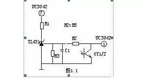
Figure. 10
When the output circuit is short-circuited, the output voltage is lost, the optocoupler OT1 is turned off, the voltage at pin 1 of the UC3842 rises to about 5V, the voltage division between R1 and R2 exceeds the reference of the TL431, causing it to turn on, the VCC potential of pin 7 of the UC3842 is pulled down, and the IC stops working. The potential of the 1 pin vanishes after the UC3842 stops operating, the TL431 does not conduct the UC3842 7, the pin's potential rises, the UC3842 restarts, and the cycle repeats. The circuit can automatically restore to its usual operational state once the short-circuit phenomenon has passed.
(3) The following figure is the medium power short circuit protection circuit, and its principle is briefly described as follows:
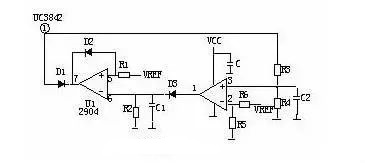
Figure. 11
When the output is short-circuited, the voltage on pin 1 of the UC3842 rises, and the potential of pin 3 of U1 is higher than that of pin 2, the comparator flips pin 1 to output a high potential to charge C1, and when the voltage across C1 exceeds the reference voltage of pin 5, pin U1 7 outputs a low potential, UC38421 is activated. When the pin falls below 1V, the UCC3842 stops operating, the output voltage drops to 0V, and the cycle repeats. When the short circuit is removed, the circuit resumes normal operation. Short-circuit protection does not work when the resistance value is incorrect, and R2 and C1 are charge and discharge time constants.
(4) The following figure is a common current limiting and short circuit protection circuit. Its working principle is briefly described as follows:
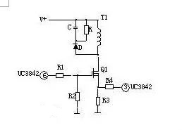
Figure. 12
The primary current of the transformer increases when the output circuit is short-circuited or over-current, the voltage drop across R3 increases, the voltage at pin 3 increases, and the output duty ratio of pin 6 of the UC3842 gradually increases. The UC3842 is turned off and has no output when the voltage at pin 3 exceeds 1V.
(5) A current transformer is used to sample current in the following protective circuit. It consumes little power but has a high cost and a complicated circuit. The following is a brief description of its functioning principle:
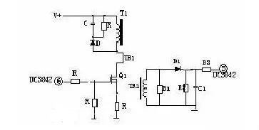
Figure. 13
The voltage induced by the TR1 secondary coil will be larger when the output circuit is short-circuited or the current is too large. The UC3842 will cease operating when pin 3 exceeds 1 volt, and the cycle will restart. The circuit will self-recover once the short-circuit or overload has passed.
7. Output current limit protection
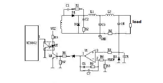
Figure. 14
The output current limiting protection circuit shown above has the following working principle: when the output current is too high, the voltage across RS (manganese copper wire) rises, the voltage of U1 3 pin is higher than the reference voltage of 2 pin, U1 1 pin. When Q1 is turned on, the optocoupler creates a photoelectric effect, lowering the voltage of pin 1 of the UC3842 and lowering the output voltage, achieving the goal of output overload current limiting.
8. The principle of output overvoltage protection circuit
When the output voltage exceeds the design value, the output overvoltage protection circuit limits the output voltage to a safe value range. The overvoltage protection circuit protects the switching power supply when the internal voltage regulation loop fails or the output overvoltage arises due to improper user action, preventing harm to the succeeding electrical equipment. The following are the most widely utilized overvoltage protection circuits:
(1) SCR trigger protection circuit:
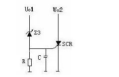
Figure. 15
When the output of Uo1 rises, the voltage regulator tube (Z3) breaks down and conducts, and the thyristor's control terminal (SCR1) receives the trigger voltage, causing the thyristor to turn on. The Uo2 voltage is short-circuited to ground, triggering the overcurrent or short-circuit protection circuits, thus shutting off the entire power supply circuit. The trigger voltage of the thyristor's control terminal is discharged to the ground through R when the output overvoltage phenomena is gone, and the thyristor returns to its unconnected condition.
(2) Photoelectric coupling protection circuit:
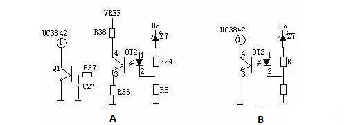
Figure. 16
When there is an overvoltage situation in Uo, the voltage regulator tube breaks down and conducts, and current flows via the optocoupler (OT2) R6 to the ground, and the optocoupler's light-emitting diode generates light, causing the phototransistor to conduct Pass, as indicated in the diagram. The base of Q1 is turned on, and the power of the 3-pin of 3842 is lowered, causing the IC to shut down and the entire power supply to stop working, Uo is zero, and the cycle repeats.
(3) Output voltage limiting protection circuit:
In the diagram below, the output voltage limiting protection circuit is depicted. The Zener tube and the optocoupler are both turned on when the output voltage rises. The channel is turned on because the base of Q1 contains a driving voltage. The UC38423's voltage rises, the output falls, and the Zener tube is turned off. UC3842③ The input voltage drops while the output voltage rises. Over time, the output voltage will stabilize within a certain range (depending on the voltage regulator value of the Zener tube).
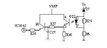
Figure. 17
(4) Output overvoltage lockout circuit:

Figure. 18
Figure A's operating principle is that as the output voltage Uo rises, the voltage regulator tube, the optocoupler, and the base of Q2 are all turned on. Q2's conduction turns on the base voltage of Q1, and the Vcc voltage is sent through R1. UC3842 3 pin is constantly high and ceases working as a result of Q2's conduction. When the voltage of U1 3 rises, the 1 pin outputs a high level, as seen in Figure B. U1 1 pin always produces a high level, Q1 is always on, and UC3842 1 pin is always low and quits working due to the presence of D1 and R. Positive responses?
9. Power Factor Correction Circuit (PFC)
(1) Schematic diagram of the principle:
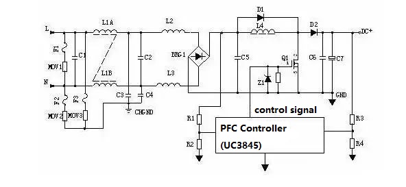
Figure. 19
(2) Working principle:
The input voltage is the EMI filter, which is made up of L1, L2, L3, and so on. BRG1 rectifies one direction to deliver PFC inductor, the other is divided by R1, R2 and supplied to PFC controller as input voltage sampling, to vary the duty of control signal ratio, that is, adjusting the turn-on and turn-off periods of Q1 to stabilize the PFC output voltage. When Q1 is on, L4 is the PFC inductor that stores energy and releases it when Q1 is off. The starter diode is D1. C6, C7 filter, D2 is the PFC rectifier diode. The post-stage circuit receives one PFC voltage, while the other is divided by R3 and R4 and delivered to the PFC controller as a sampling of the PFC output voltage to change the duty cycle of the control signal and stabilize the PFC output voltage.
10. Input overvoltage and undervoltage protection
(1) Schematic diagram:
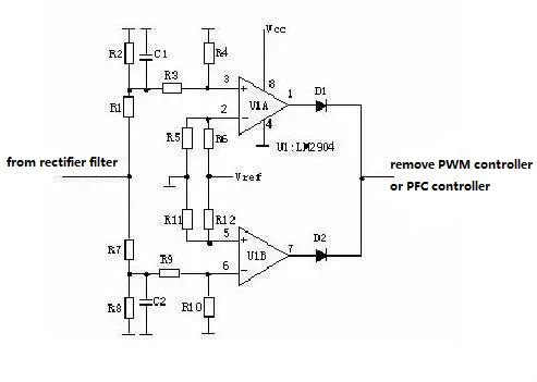
Figure. 20
(2) Working principle:
AC input and DC input switching power supplies use the same input over-voltage protection principle. The protection circuit's sampling voltage is derived from the input filtered voltage. The sampling voltage is split into two channels, one of which is divided by R1, R2, R3, R4, and then fed into comparator pin 3. The comparator pin 1 outputs a high level to regulate the main controller to turn it off if the sampling voltage is higher than the reference voltage of pin 2, and the power supply has no output. The other path is separated by R7, R8, R9, and R10 before being fed into comparato
1. What is a feedback?
Feedback is to collect the output signal back to the input end of the signal so that the output signal can output the useful signal we want according to certain requirements
2. What are the commonly used electrical appliances for short circuit protection in the circuit?
Commonly used electrical appliances for short-circuit protection in circuits include fuses and overcurrent protection devices.
3. How does a flyback circuit work?
The flyback switching power supply adopts a dual-loop feedback (output DC voltage isolation sampling feedback loop and primary coil magnetizing peak current sampling feedback loop) control system with good stability, which can be controlled by the PWM (pulse width modulator) of the switching power supply. ) quickly adjust the pulse duty cycle, so as to effectively adjust the output voltage of the previous cycle and the peak current of the primary coil magnetization in each cycle to achieve the purpose of stabilizing the output voltage.
 LLC Converter with Planar Matrix Transformer for High-Current-High-Power ApplicationsSaumitra Jagdale15 March 20244761
The rise of data centres in recent years, driven by cloud computing and big data, has caused a significant increase in electricity consumption. In the United States alone, it exceeded 70 billion kWh by 2014, making up 1.8% of total national electricity usage.
Read More Enhancing Frequency Stability in Modern Distributed Power SystemsRakesh Kumar, Ph.D.21 September 20244261
The article discusses the importance of primary frequency regulation in maintaining grid stability. It also explores battery energy storage systems, virtual synchronous generators, and advanced control strategies to enhance frequency stability in power systems.
Read More The Impact of SMPS on LED Lighting and Diverse IndustriesUTMEL05 June 20252618
Switched-Mode Power Supplies (SMPS) enhance LED lighting and industries by improving energy efficiency, reliability, and sustainability across diverse applications.
Read More What is Uninterruptible Power Supply (UPS)?UTMEL08 April 20215274
UPS is an uninterruptible power supply containing the energy storage device. It is mainly used to give a part of a device with a higher power stability, providing uninterrupted power supplies.
Read More Switch-mode Power Supply BasicsUTMEL14 December 20207884
Switched-mode Power Supply (SMPS), also known as switching converter, is a high-frequency electric energy conversion device and a type of power supply. Its function is to convert a level of voltage into the voltage or current required by the user through different forms of architecture.
Read More
Subscribe to Utmel !
![3RT20353AP00]() 3RT20353AP00
3RT20353AP00Siemens
![3RH21221BE40]() 3RH21221BE40
3RH21221BE40Siemens
![3RT20363AP00]() 3RT20363AP00
3RT20363AP00Siemens
![3RH21402BM40]() 3RH21402BM40
3RH21402BM40Siemens
![3RT23361AB00]() 3RT23361AB00
3RT23361AB00Siemens
![3RT20242AC20]() 3RT20242AC20
3RT20242AC20Siemens
![3RT20232AC20]() 3RT20232AC20
3RT20232AC20Siemens
![3RT20383AP00]() 3RT20383AP00
3RT20383AP00Siemens
![3RT20373AF00]() 3RT20373AF00
3RT20373AF00Siemens
![3RT23251AP00]() 3RT23251AP00
3RT23251AP00Siemens


 Product
 Brand
Brand Articles
 Tools
Tools


