Product
 Brand
Brand Articles
 Tools
Tools
Image Sensor: How do CCD and CMOS Sensors work?
Image Sensors Explained: How CCD and CMOS Sensors works? CCD vs CMOS
Catalog
Ⅰ Introduction
An image sensor, or photosensitive element, is a device that converts an optical image into an electronic signal. It is widely used in digital cameras, smartphones, security systems, medical imaging equipment, and other electronic optical devices. The image sensor uses the photoelectric conversion function of the photoelectric device to convert the light image on the photosensitive surface into an electrical signal in a proportional relationship with the light image. Compared to photosensitive elements such as photodiodes and phototransistors, an image sensor is a functional device that divides the light image on its light-receiving surface into many small units and converts it into usable electrical signals.
Image sensors are divided into light guide camera tubes and solid-state image sensors. Compared with light guide camera tubes, solid-state image sensors have the characteristics of small size, light weight, high integration, high resolution, low power consumption, long life, and competitive pricing. As of 2025, solid-state sensors have almost completely replaced traditional camera tubes in commercial applications. [6]
The photosensitive device is the core component of industrial and consumer cameras. There are two primary types of image sensors: CMOS (Complementary Metal-Oxide-Semiconductor) and CCD (Charge-Coupled Device). Historically, CCD sensors dominated the market due to their superior image quality, low noise characteristics, and excellent color reproduction. CCD technology has been widely used in high-end fields such as transportation, medical imaging, and scientific research. However, due to higher manufacturing costs and greater power consumption, CCD's market share has significantly declined since the 2010s. [3]
CMOS sensors utilize standard semiconductor manufacturing processes, offering advantages in integration, power consumption, processing speed, and cost-effectiveness. In recent years, CMOS technology has made remarkable advances in wide dynamic range, low-light performance, and overall image quality. By 2025, CMOS sensors have achieved performance levels that rival or exceed CCD in most applications, leading to CMOS becoming the dominant technology in smartphones, digital cameras, automotive imaging, and even many scientific applications. [2] [3]
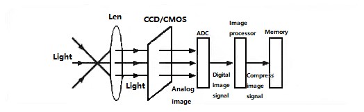
Figure 1: Working process of the image sensor
An image sensor is a semiconductor device that converts optical images into digital signals. The tiny photosensitive material implanted on the sensor is called a pixel. The more pixels present on a sensor, the higher the resolution of the captured image. Modern image sensors can contain anywhere from a few megapixels in basic applications to over 100 megapixels in high-end professional cameras. The sensor functions similarly to traditional film but converts image information into digital signals through photoelectric conversion and analog-to-digital conversion processes. [5]
Ⅱ CCD
1 Definition of CCD Image Sensor
CCD (Charge-Coupled Device) is a sophisticated technical component historically used in high-quality photography and imaging applications. CCD was successfully developed at Bell Labs in 1969 by Willard Boyle and George E. Smith, who later received the Nobel Prize in Physics in 2009 for this invention. Mass production began in the 1970s, led by Japanese companies and other manufacturers. CCD technology has evolved significantly over its more than 50-year history. [4]
CCD sensors can be divided into two main types: Linear and Area. Linear CCDs are used in image scanners, fax machines, and spectroscopy equipment, while area CCDs have been primarily used in digital cameras (DSC), camcorders, surveillance systems, and scientific imaging applications. However, as of 2025, area CCD sensors have been largely replaced by CMOS sensors in consumer applications, though they remain in use for specialized scientific and industrial applications. [3] [9]
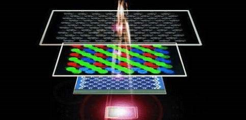
Figure 2: Composition of CCD sensor
CCD technology replaced traditional film in the digital imaging era. Its working principle evolved from the concept that chemical substances on film sense light. CCD is manufactured from high-sensitivity semiconductor materials, which convert light into electric charge. This charge is then converted into digital signals through an analog-to-digital converter chip. The digital signals are compressed and stored in the camera's internal flash memory or storage media, allowing easy data transfer to computers for post-processing and editing.
2 Working Principle of CCD Image Sensor
A CCD is composed of many photosensitive units, typically measured in megapixels. When the surface of the CCD is exposed to light, each photosensitive unit reflects charge proportional to the light intensity on the component. The signals generated by all photosensitive units are combined to form a complete image. Unlike CMOS sensors where each pixel has its own amplifier, CCD sensors transfer charges across the chip to a single output node, which is then amplified and converted to a voltage signal. [5] [7]
The basic unit of a CCD is a MOS capacitor, which stores electric charge. Taking P-type silicon as an example, a silicon dioxide (SiO₂) layer is formed on the surface through oxidation on a P-type silicon substrate, and then a metal layer is deposited on the SiO₂ as a gate electrode. The majority carriers in P-type silicon are positively charged holes, while minority carriers are negatively charged electrons.
When a positive voltage is applied to the metal electrode, its electric field repels or attracts carriers through the SiO₂ insulating layer. The positively charged holes are repelled away from the electrode, while negatively charged minority carriers (electrons) accumulate near the SiO₂ layer, forming a depletion layer. This phenomenon creates a trap for electrons, also called an electron potential well. Once electrons enter this potential well, they remain trapped until deliberately transferred.
When the device is exposed to light (photons can be injected through the SiO₂ layer between the electrode gaps or through the thin P-type silicon substrate), the photon energy is absorbed by the semiconductor, generating electron-hole pairs. The electrons are attracted and stored in the potential well, while holes are swept away. The number of electrons collected is proportional to the light intensity—stronger light results in more electrons in the potential well. This process converts light intensity into charge quantity, achieving photoelectric conversion. The electrons collected in the potential well are stored and retained even after light exposure ceases, realizing light signal memory.

Figure 3: CCD structure and working principle diagram
In essence, this structure is a tiny MOS capacitor array forming pixels that can be "photosensitive" and retain a "latent image." The photosensitive function accumulates charge from photogenerated electrons proportional to light intensity, and the latent image is formed by the varying charge levels in each capacitor. By systematically transferring the charge from each capacitor sequentially to an output node, line-by-line and frame-by-frame image readout is achieved. This charge transfer mechanism is the fundamental characteristic that gives CCD (Charge-Coupled Device) its name. [7]
3 Features of CCD Image Sensor
High Resolution: The pixel size is at the micrometer (μm) level, capable of sensing and identifying fine details to improve image quality. CCD sensors have evolved from early resolutions of around 100,000 pixels to modern scientific CCDs with 4-16 megapixels or more, with pixel sizes ranging from 1 inch to 1/9 inch formats.
Low Noise & High Sensitivity: CCD sensors have very low read noise and dark current noise, resulting in excellent signal-to-noise ratio (SNR) and high sensitivity. They can detect incident light with very low intensity without signal degradation, making CCDs less constrained by ambient lighting conditions. This characteristic remains one of CCD's key advantages in low-light scientific applications. [3] [9]
Wide Dynamic Range: CCD sensors can simultaneously detect and distinguish both strong and weak light signals, improving system performance across varied lighting environments. This prevents signal contrast issues caused by large brightness differences.
Excellent Linearity: The incident light intensity and output signal size maintain a strong proportional relationship. Object information is faithfully preserved without loss, reducing the need for signal compensation processing.
High Quantum Efficiency: Very weak incident light can be recorded. When combined with image intensifier tubes and light amplifiers, distant scenes can be detected even at night, making CCDs valuable for astronomy and night vision applications.
Large Field of View: Large-area CCD chips can be manufactured using semiconductor technology. Full-frame 35mm CCDs equivalent to traditional film size have been used in professional digital cameras, though this application has largely transitioned to CMOS sensors in recent years.
Broad Spectral Response: CCDs can detect light across a wide wavelength range (from ultraviolet to near-infrared), increasing system flexibility and expanding application areas.
Low Image Distortion: CCD sensors faithfully reproduce original object information with minimal geometric distortion.
Compact Size and Light Weight: CCDs are characterized by small size and light weight, making them easily integrated into satellites, drones, and various navigation systems.
Excellent Charge Transfer Efficiency: This efficiency factor directly affects signal-to-noise ratio and resolution. High charge transfer efficiency (typically >99.99%) ensures that images remain sharp and clear. Poor charge transfer efficiency results in image blur and reduced quality.
Ⅲ CMOS
1 Definition of CMOS Image Sensor
CMOS (Complementary Metal-Oxide-Semiconductor) technology utilizes standard semiconductor manufacturing processes common in integrated circuit production. It is primarily a semiconductor made of silicon and incorporating both n-type and p-type transistors. These complementary transistors work together to minimize power consumption—when one transistor is on, the other is off, resulting in very low static power consumption. This fundamental characteristic makes CMOS technology highly energy-efficient. [2]
A CMOS image sensor is a typical solid-state imaging sensor that shares a common historical origin with CCD. While both technologies perform photoelectric conversion, they differ fundamentally in their architecture and signal processing methods. CMOS image sensors typically integrate multiple functions on a single chip, including the image sensor cell array, row drivers, column drivers, timing control logic, analog-to-digital (AD) converters, data bus output interfaces, and control interfaces. This high level of integration is a key advantage of CMOS technology. [5]
The working process of a CMOS image sensor can be divided into four main stages: reset, photoelectric conversion, integration (charge accumulation), and readout. Unlike CCD sensors that transfer charges sequentially across the entire array, CMOS sensors allow random access to individual pixels, enabling faster readout speeds and more flexible operation modes.
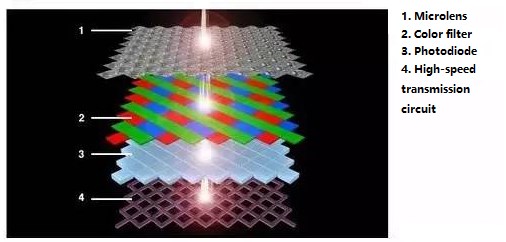
Figure 4: Composition of CMOS sensor
The photoelectric conversion function of CMOS is fundamentally similar to that of CCD—both convert photons into electrons. The primary difference lies in how the electrical information is processed and transmitted after photoelectric conversion. In CCD sensors, charges are transferred sequentially across the sensor to a single output amplifier. In CMOS sensors, each pixel (or column of pixels) contains its own amplification circuitry, allowing parallel signal processing and faster readout speeds. [2] [7]
2 Working Principle of CMOS Image Sensor
(1) The Pixel Structure of the MOS Transistor
To understand CMOS image sensors, we must first examine the fundamental building block—the pixel structure based on MOS transistors. A typical CMOS pixel consists of a photodiode for light detection and multiple transistors for signal amplification, reset, and selection functions.
The MOS transistor and photodiode together constitute the structural unit equivalent to one pixel. During the light integration period, the reset transistor is turned off, and the photodiode generates charge carriers proportional to the incident light intensity. These carriers are stored at the photodiode junction (position ① in the figure below), causing the voltage at this node to change proportionally to the light intensity.
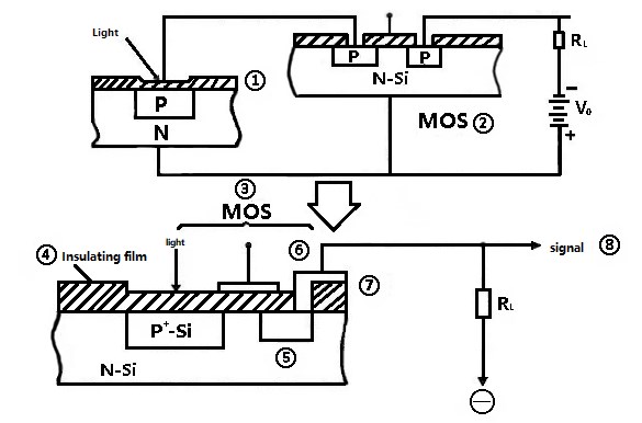
Figure 5: MOS transistor pixel structure
When the integration period ends, a scan pulse is applied to the row select transistor to activate the pixel. The source follower transistor amplifies the signal, and the voltage corresponding to the accumulated charge is read out through the column line. After readout, a reset pulse is applied to restore the photodiode to its reference potential, preparing it for the next integration cycle. This pixel-level amplification is a key distinguishing feature of CMOS sensors compared to CCDs. [5]
(2) CMOS Image Sensor Array Structure
Multiple MOS transistor pixel structures form a CMOS image sensor array. This is where the CMOS image sensor begins to sense and process light information. The CMOS image sensor array structure consists of a horizontal (column) decoder/multiplexer, a vertical (row) decoder, and the CMOS pixel array itself.
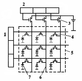
Figure 6: CMOS image sensor array structure
(1-vertical shift register; 2-horizontal shift register; 3-horizontal scan switch; 4-vertical scan switch; 5-image sensor array; 6-signal line; 7-image sensor)
As mentioned above, each MOS transistor functions as a switch under the control of horizontal and vertical scanning circuits. The horizontal decoder sequentially activates column readout circuits from left to right (column addressing), while the vertical decoder sequentially selects each row of the array (row addressing). This X-Y addressing scheme allows random access to any pixel or group of pixels.
Each pixel comprises a photodiode for light detection and multiple MOS transistors for signal processing. The row select signal activates an entire row of pixels simultaneously, and their signals are read out in parallel through column amplifiers. This parallel architecture enables much faster readout speeds compared to CCD's serial charge transfer, making CMOS sensors ideal for high-speed imaging applications. [2]
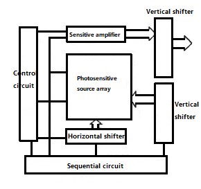
Figure 7: CMOS image sensor array working diagram
The illuminated photodiode generates charge carriers that accumulate during the integration period, changing the voltage at the sensing node. This accumulation process represents the signal integration. When the row is selected for readout, the pixel's source follower transistor converts this voltage change into a current signal that flows through the column line to the readout circuitry. The magnitude of the video signal formed is proportional to the light intensity on the pixel, maintaining the linear relationship between light and electrical signal.
(3) Three Steps to Understanding the Workflow of a CMOS Image Sensor
According to the functional block diagram of the CMOS image sensor, the workflow can be divided into three main steps:

Figure 8: Functional block diagram of CMOS image sensor
Step 1: External light illuminates the pixel array and photoelectric conversion occurs, generating corresponding charge in each pixel unit.
The scene is focused onto the image sensor array through an imaging lens. The image sensor array is a two-dimensional pixel array where each pixel contains a photodiode. The photodiode in each pixel converts the incident light intensity into an electrical charge through the photoelectric effect. The amount of charge generated is directly proportional to the number of photons received and the integration time.
Step 2: The desired pixel is selected through the row selection circuit and column selection circuit, and the electrical signal from the pixel is read out.
During the selection process, the row selection logic unit can scan the pixel array row by row, in interlaced fashion, or even access specific regions of interest (ROI). The column selection logic works in coordination with row selection. Together, the row and column selection circuits enable flexible windowing and region-of-interest extraction, which is particularly useful for high-speed imaging applications where only a portion of the sensor needs to be read out. [2]
Step 3: The pixel signals undergo signal processing and are output as digital data.
The analog image signal from each row of pixels is transmitted through column signal buses to corresponding analog signal processing units and analog-to-digital (A/D) converters, where it is converted into digital image signals for output. The primary function of the analog signal processing unit is to amplify the signal and improve the signal-to-noise ratio through various noise reduction techniques.
The pixel electrical signal is amplified and sent to a Correlated Double Sampling (CDS) circuit for processing. Correlated double sampling is an important technique used in high-quality sensors to eliminate various types of interference and noise. The basic principle involves sampling the pixel signal twice—once immediately after reset (to capture the reset noise) and once after charge integration (to capture the signal plus reset noise). The difference between these two samples removes correlated noise components.
This method effectively reduces kTC noise (thermal reset noise), reset noise, and Fixed Pattern Noise (FPN). It can also reduce 1/f (flicker) noise and significantly improve the signal-to-noise ratio. Modern CMOS sensors often employ more advanced techniques such as multiple sampling or digital CDS to further enhance image quality. The signal then undergoes additional processing including integration, amplification, sampling, and hold functions before being sent to an analog-to-digital converter and output as a digital signal. [5]
Additionally, to create a functional camera system, the chip must contain various control circuits such as exposure time control, automatic gain control (AGC), and white balance adjustment. To ensure all circuit components operate in proper synchronization, multiple timing control signals are required. Modern CMOS sensors also output various timing signals including synchronization signals, line start signals, and frame start signals to facilitate system integration and application development.
3 Modern Advancements in CMOS Technology
Since 2020, CMOS sensor technology has made remarkable progress, addressing many of the historical limitations that once made CCD the preferred choice for high-quality imaging. Key advancements include: [3]
Backside Illumination (BSI) Technology: BSI CMOS sensors place the photodiode layer above the transistor circuitry, allowing more light to reach the photosensitive area. This significantly improves quantum efficiency and low-light performance, achieving sensitivity levels that rival or exceed traditional CCD sensors.
Stacked CMOS Architecture: Modern stacked CMOS sensors separate the pixel array and signal processing circuits onto different silicon layers connected by through-silicon vias (TSVs). This architecture allows for more sophisticated on-chip processing while maintaining small pixel sizes and high fill factors.
Global Shutter CMOS: Unlike traditional rolling shutter CMOS sensors, global shutter technology exposes all pixels simultaneously, eliminating motion artifacts. This makes CMOS suitable for high-speed imaging applications previously dominated by CCD sensors. [2]
Enhanced Dynamic Range: Modern CMOS sensors employ techniques such as dual conversion gain, multiple exposure HDR, and advanced pixel architectures to achieve dynamic ranges exceeding 120 dB, surpassing most CCD sensors.
On-Chip AI Processing: Advanced CMOS sensors now integrate artificial intelligence and machine learning capabilities directly on the sensor chip, enabling real-time image analysis, object detection, and scene recognition with minimal power consumption.
Scientific CMOS (sCMOS): Specifically designed for scientific imaging applications, sCMOS sensors combine the low noise and high quantum efficiency of CCD with the speed and flexibility of CMOS. By 2025, sCMOS sensors have become the preferred choice for many scientific applications including microscopy, astronomy, and high-speed spectroscopy. [3]
Ⅳ CCD vs CMOS: Current Market Status (2025)
The image sensor market has undergone dramatic transformation over the past decade. As of 2025, CMOS sensors dominate the market with over 95% market share across all imaging applications. This represents a complete reversal from the early 2000s when CCD sensors held the majority of the high-quality imaging market. [6]
Consumer Electronics: CMOS sensors have completely replaced CCD in smartphones, tablets, webcams, and consumer digital cameras. Modern smartphone cameras utilize advanced stacked CMOS sensors with computational photography capabilities, achieving image quality that rivals dedicated cameras from just a decade ago.
Professional Photography: High-end mirrorless and DSLR cameras now exclusively use large-format CMOS sensors, with resolutions ranging from 24 to over 100 megapixels. These sensors offer exceptional image quality, fast readout speeds, and advanced features like in-body image stabilization and real-time eye-tracking autofocus.
Industrial and Machine Vision: CMOS sensors have become the standard in industrial inspection, robotics, and autonomous vehicles due to their high frame rates, low power consumption, and ability to integrate processing functions on-chip. Global shutter CMOS sensors have addressed the motion artifact issues that previously favored CCD in these applications. [2]
Scientific Imaging: This remains one of the few areas where CCD sensors maintain a presence, particularly in specialized applications requiring extremely low noise and long exposure times. However, even in scientific imaging, sCMOS sensors have captured significant market share due to their combination of low noise, high speed, and large field of view. Electron-Multiplying CCD (EMCCD) sensors continue to be used in ultra-low-light applications such as single-molecule fluorescence microscopy, but their market is shrinking as CMOS technology advances. [3] [9]
Automotive Applications: CMOS sensors dominate automotive imaging for applications including advanced driver assistance systems (ADAS), surround-view cameras, driver monitoring systems, and autonomous driving. The automotive image sensor market is one of the fastest-growing segments, with CMOS sensors offering the necessary combination of performance, reliability, and cost-effectiveness.
Medical Imaging: While CCD sensors were once prevalent in medical X-ray imaging and endoscopy, CMOS sensors have increasingly replaced them due to superior integration capabilities, lower power consumption, and the ability to incorporate advanced image processing functions on-chip.
Ⅴ Conclusion
The evolution of image sensor technology over the past 50+ years represents one of the most significant technological transformations in modern electronics. While CCD sensors dominated imaging applications from the 1970s through the early 2000s due to their superior image quality and low noise characteristics, CMOS technology has undergone remarkable advancement to become the dominant technology by 2025. [4]
CCD sensors provided excellent image quality, superior noise performance, and flexibility in camera design. Although system size and complexity increased due to external circuitry requirements, this allowed greater flexibility in circuit design and optimization of camera performance. Today, CCD sensors remain relevant primarily in specialized scientific applications requiring extremely low noise, long exposure capabilities, and exceptional linearity—such as astronomy, high-precision spectroscopy, and certain medical imaging applications. Electron-Multiplying CCDs (EMCCDs) continue to serve niche applications in ultra-low-light imaging where their unique amplification mechanism provides advantages. [9]
CMOS sensors can be manufactured using contemporary large-scale semiconductor integrated circuit production processes, offering high yield, high integration, low power consumption, and cost-effectiveness. After decades of development, CMOS technology has overcome its early limitations and now matches or exceeds CCD performance in virtually all aspects of image quality. Modern CMOS sensors incorporate advanced features such as backside illumination, stacked architectures, global shutter operation, on-chip AI processing, and exceptional dynamic range. [2] [3]
CMOS sensors are now the preferred choice across a vast range of applications: consumer electronics (smartphones, tablets, laptops), professional photography, industrial machine vision, automotive imaging, security and surveillance, medical imaging, and increasingly in scientific research. The ability to integrate sophisticated signal processing, artificial intelligence, and system control functions directly on the sensor chip provides CMOS with unmatched versatility and functionality. [5] [6]
Looking forward, CMOS technology continues to advance with developments in quantum dot sensors, organic photodetectors, event-based vision sensors, and further integration of computational imaging and AI capabilities. The future of imaging belongs to CMOS, while CCD technology will remain a specialized tool for specific applications where its unique characteristics provide irreplaceable advantages.
Key Takeaways (2025):
CMOS sensors now dominate with >95% market share across all imaging applications
Modern CMOS technology (BSI, stacked sensors, global shutter) rivals or exceeds CCD performance
CCD remains relevant only in specialized scientific applications requiring extreme low-noise performance
sCMOS (Scientific CMOS) has replaced CCD in many research applications
Future developments focus on computational imaging, AI integration, and novel sensor architectures
Related Article Recommendations:
Introduction to Types of Motion Sensors
Introduction to Temperature Sensors
Article Update Information:
Originally published: 2020
Last updated: October 2025
Updates include: Current market statistics (2025), modern CMOS advancements (BSI, stacked sensors, global shutter, sCMOS), corrected technical information, updated application scenarios, and current industry trends. All technical specifications and market data have been verified against 2024-2025 sources.
Sources Referenced:
[2]: Wevolver - CCD vs CMOS Image Sensors Comprehensive Guide
[3]: Bio-Radiations - Advancements in CMOS Sensors for Scientific Imaging
[4]: CMOS Sensor Inc - CCD vs CMOS Historical Review
[5]: Canon Europe - Camera Sensors Explained
[6]: Market.us - Image Sensor Statistics and Facts (2025)
[7]: Basler - CCD vs CMOS Differences
[9]: Teledyne Vision Solutions - CCD vs CMOS Technical Comparison
 UTMEL
UTMEL
We are the professional distributor of electronic components, providing a large variety of products to save you a lot of time, effort, and cost with our efficient self-customized service. careful order preparation fast delivery service
1.What does an image sensor do?
An image sensor is a device that allows the camera to convert photons – that is, light – into electrical signals that can be interpreted by the device. The first digital cameras used charge-coupled devices, facilitating movement of the electrical charge through the device so it could be modulated.
2.How much is a image sensor?
CMOS image sensors are produced in bulk for many low-end applications, e.g., low-end digital still cameras, PDAs, and mobile phones, with a cost of production ranging from $4–$10, depending on the application.
3.How do camera sensors work?
The most basic way you can understand how a sensor works is when the shutter opens, the sensor captures the photons that hit it and that is converted to an electrical signal that the processor in the camera reads and interprets as colors. This information is then stitched together to form an image.
4.What is image sensor in CCTV camera?
An image sensor is the part of your IP camera that captures the light hitting the camera lens and turns it into electrical signals, which get recorded as the video you see when monitoring your system.
5.How does sensor size affect image quality?
The larger your camera's sensor, the larger the photosites, the more resultant megapixels, which allow for a better image and a higher resolution. High resolution is important to ensure that your images are high quality even when you blow up a photo to a larger size.
 The Key Role of Electronic Components in IoT DevicesUTMEL01 September 20235736
The article discusses the pivotal role of electronic components in Internet of Things (IoT) devices. IoT devices work by capturing real-world data using sensors, processing it through a microcontroller, and then sending it to the cloud for further analysis.
Read More How to Identify the Perfect Proximity Sensor for Your ApplicationUTMEL19 July 20251644
Find the best proximity sensors for your project by evaluating material, sensing range, environment, and system needs to ensure optimal performance and reliability.
Read More Trusted Vibration Sensors for Homeowners and Industry ProfessionalsUTMEL17 July 20251296
Compare top vibration sensors for home and industrial use. Find trusted options for security, predictive maintenance, and equipment protection.
Read More Wiring and Mounting Photoelectric Sensors in 2025UTMEL15 July 20251502
Wire and mount photoelectric sensors in 2025 with step-by-step safety, wiring, and alignment tips for reliable installation and optimal sensor performance.
Read More Essential Tips for Picking the Best Gas SensorUTMEL15 July 20252858
Find out how to select gas sensors by matching target gases, environment, and compliance needs for reliable and accurate gas detection in any setting.
Read More
Subscribe to Utmel !