Product
 Brand
Brand Articles
 Tools
Tools
How do Transistors Work?

How do Transistors work?
Catalog
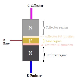
The transistor is one of the basic semiconductor components, which has the function of current amplification and is the core component of the electronic circuit. The transistor is made of two PN junctions very close to each other on a semiconductor substrate. The two PN junctions divide the whole semiconductor into three parts. The middle part is the base area, and the two sides are the emitter and collector areas. PNP And NPN are the two kinds of arrangements.
Ⅰ The core structure of transistors

transistor
The core of the transistor is the "PN" junction, which is two back-to-back PN junctions. The PN junction can be a combination of NPN or a combination of PNP. Since silicon NPN type is the mainstream of transistors, the following content mainly takes silicon NPN type transistor as an example.
Schematic diagram of NPN transistor structure
The manufacturing process of the silicon NPN transistor:

Die structure section view:

Ⅱ The operation status of transistors
1 Cutoff state
When the voltage applied to the emitter junction of the transistor is less than the conduction voltage of the PN junction, the base current, the collector current, and the emitter current are zero. The transistor loses its current amplification effect, and the collector and emitter are equal in the off state of the switch, which we call the transistor in the cutoff state.
2 Active state
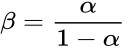
The transistor operates in active region when the emitter junction of the transistor is forward biased, and the collector junction is reverse biased. In the active region, the voltage applied to the emitter junction of the transistor is greater than the turn-on voltage of the PN junction. And the base current controls the collector current, so that the transistor acts as an amplifier, and its current amplification factor β=ΔIc/ΔIb. We call the transistor is in an active state.
3 Saturation state
When the voltage applied to the emitter junction of the transistor is greater than the conduction voltage of the PN junction, and when the base current increases to a certain extent, the collector current no longer increases with the increase of the base current. At this time, the transistor loses its current amplification effect. The voltage between the collector and the emitter is very small, and the collector and emitter are equivalent to the On state of the switch. This state of the transistor is called the saturated conduction state.
According to the voltage level of each electrode when the transistor is working, the working state of the transistor can be judged. Electronic maintenance personnel often use a multimeter to measure the voltage of each pin of the transistor during the maintenance process to determine the working condition and the working state of the transistor.
Ⅲ Theoretical working principle of transistors
There are two types of transistors according to materials: germanium tubes and silicon tubes. Each of them has two structural forms, NPN and PNP, but the most used are silicon NPN and germanium PNP transistors. N-type semiconductors add phosphorus in high-purity silicon to replace some silicon atoms to generate free electron conduction under-voltage stimulation. P means positive. P-type semiconductors add boron to replace silicon, which generates a large number of holes to facilitate conduction. Except for the difference in power supply polarity, the two work principles are the same. The following only introduces the current amplification principle of NPN silicon tubes.

NPN transistor and PNP transistor
An NPN transistor is composed of two N-type semiconductors and a P-type semiconductor in the middle. The PN junction formed between the emitter region and the base region is called the emitter junction, and the PN junction formed by the collector region and the base region is called the collector junction. The three leads are called Emitter e, Base b, and Collector c.
When the potential at point b is higher than the potential at point e by a few volts, the emitter junction is in a forward-biased state. When the potential at point C is a few volts higher than the potential at point b, the collector junction is in a reverse-biased state, and the collector power Ec is higher than the base power Eb.
When manufacturing the transistor, the majority carrier concentration in the emitter region is deliberately made larger than that in the base region. At the same time, the base region is made very thin, and the impurity content must be strictly controlled. In this way, once the power is turned on, the emitter junction is positively biased. The majority carriers (electrons) in the emitter region and the majority carriers (holes) in the base region easily diffuse to each other across the emitter junction. The concentration base of the former is greater than the latter, so the current through the emitter junction is basically a flow of electrons, which is called the emitter electron flow.
Due to the thin base area and the reverse bias of the collector junction, most of the electrons injected into the base area cross the collector junction and enter the collector area to form a collector current Ic, leaving only a few (1-10%) electrons. These electrons are recombined in the holes of the base area, and the recombined holes in the base area are recharged by the base power supply Eb, thus forming the base current Ibo. According to the principle of current continuity:
Ie=Ib+Ic
This means that by adding a small Ib to the base, a larger Ic can be obtained on the collector. This is the so-called current amplification. Ic and Ib maintain a certain proportional relationship, namely:
β1=Ic/Ib
In the formula: β1 is DC amplification factor,
The ratio of the change in collector current △Ic to the change in base current △Ib is:
β= △Ic/△Ib
In the formula, βis called the AC amplification factor. Because the values of β1 and β are not much different at low frequencies, sometimes for convenience, the two are not strictly distinguished, and the β value is about tens to more than one hundred.
α1=Ic/Ie (Ic and Ie are the currents in the DC path)
The formula: α1 is also called the DC amplification factor, which is generally used in a common base configuration amplifier circuit to describe the relationship between the emitter current and the collector current.
α =△Ic/△Ie
The α in the expression is the magnification of the AC common base current. Similarly, there is not much difference between α and α1 when a small signal is input.
For two magnifications describing the current relationship, the relationship is:
The current amplification effect of the transistor is actually to use the small change of the base current to control the huge change of the collector current. The transistor is a kind of current amplifier device, but in actual use, the current amplifier effect of the transistor is often transformed into a voltage amplifier effect through a resistor.
Ⅳ Amplification principle of transistors
1 The emitter emits electrons to the base
The power supply Ub is added to the emission junction through the resistor Rb. The emission junction is forward biased, and the majority of carriers (free electrons) in the emission area continuously cross the emission junction and enter the base area, forming an emitter current Ie. At the same time, the majority of carriers in the base region diffuse to the emission region, but since the majority carrier concentration is much lower than the carrier concentration in the emission region, this current can be ignored, so it can be considered that the emission junction is mainly electron flow.
2 The diffusion and recombination of electrons in the base
After the electrons enter the base area, they are first concentrated near the emitter junction, and gradually forming an electron concentration difference. Because of the concentration difference, the electron flow is promoted to diffuse in the base to the collector junction and is drawn into the collector by the collector junction electric field. It is called the collector current Ic. There is also a small part of electrons (because the base region is very thin) recombined with the holes in the base region, and the ratio of the diffused electron flow to the composite electron flow determines the amplification ability of the transistor.
3 Collect electrons in the collector
Since the reverse voltage applied to the collector junction is very large, the electric field force generated by this reverse voltage will prevent the electrons in the collector region from diffusing to the base region. At the same time, the electrons diffused near the collector junction will be drawn into the collector region to form the main collector current Icn. In addition, the minority carriers (holes) in the collector region will also drift and flow to the base region to form a reverse saturation current, which is represented by Icbo. Its value is very small, but it is extremely sensitive to temperature.
Ⅴ Amplifier circuit of transistors
1 Basic structure
The basic amplifier circuit is the basic unit that constitutes a complex amplifier circuit. It uses the characteristics of bipolar semiconductor transistor input current to control output current or the characteristics of field-effect semiconductor transistor input voltage to control output current to realize signal amplification.

Basic amplifier circuit
The basic amplifier circuit generally refers to an amplifier circuit composed of a transistor or a field effect tube. From the circuit point of view, the basic amplifier circuit can be seen as a dual-port network. The role of amplification is reflected in the following aspects:
1) The amplifier circuit mainly uses the control function of the transistor or the field-effect tube to amplify the weak signal. The output signal is amplified in the amplitude of the voltage or current, and the energy of the output signal is strengthened.
2) The energy of the output signal is actually provided by the DC power supply, but it is converted into signal energy through the control of the transistor and supplied to the load.
2 Circuit composition
There are three different transistor circuit configurations: common emitter, common base and common collector. These three circuit configurations have different characteristics. Various configurations of a single transistor amplifier are possible.
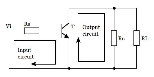
Common emitter circuit, input loop, and output loop have passed the emitter of the transistor
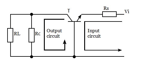
Common base circuit, the input loop, and output loop have passed the base of the transistor
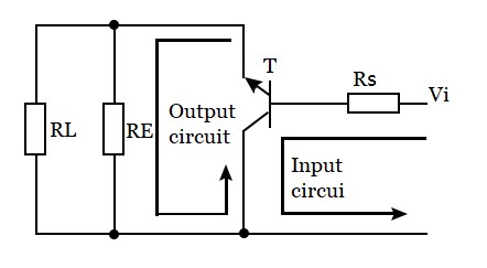
Common collector circuit, input circuit, and output circuit have passed the collector of the transistor
Common emitter amplifier circuit
The basic amplifier circuit of common emitter configuration is that the input signal is added between the base and the emitter, and the coupling capacitors C1 and Ce are regarded as short-circuiting the AC signal. The output signal is taken out from the collector to the ground, the direct current is separated by the coupling capacitor C2, and only the alternating current signal is added to the load resistance RL. The common emission configuration of the amplifier circuit actually refers to the common emission configuration of the transistor in the amplifier circuit.
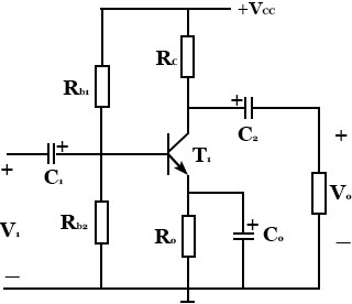
Common emitter configuration amplifier circuit
When the input signal is zero, the DC power supply provides DC base current and DC collector current for the transistor through each bias resistor and forms a certain DC voltage between the three poles of the transistor. Due to the DC blocking effect of the coupling capacitor, the DC voltage cannot reach the input and output terminals of the amplifier circuit.
When the input AC signal is added to the transmitter junction of the transistor through the coupling capacitors C1 and Ce, the voltage on the transmitter junction becomes a superposition of AC and DC. The signal situation in the amplifier circuit is more complicated. The symbols of each signal are stipulated as follows: due to the current amplification effect of the transistor, ic is dozens of times larger than ib. Generally speaking, as long as the circuit parameters are set appropriately, the output voltage can be much higher than the input voltage. A part of the AC in uCE reaches the load resistance through the coupling capacitor and forms the output voltage.
It can be seen that the DC signal of the collector of the transistor in the amplifier circuit does not change with the input signal and the AC signal changes with the input signal. In the amplification process, the collector AC signal is superimposed on the DC signal, and only the AC signal is extracted from the output terminal through the coupling capacitor. Therefore, when analyzing the amplifier circuit, the method of separating the AC and DC signals can be used, which can be divided into a DC path and an AC path for analysis.
Related Articles:
 UTMEL
UTMEL
We are the professional distributor of electronic components, providing a large variety of products to save you a lot of time, effort, and cost with our efficient self-customized service. careful order preparation fast delivery service
1.What is the basic function of a transistor?
A transistor is a semiconductor device used to amplify or switch electronic signals and electrical power. Transistors are one of the basic building blocks of modern electronics. It is composed of semiconductor material usually with at least three terminals for connection to an external circuit.
2.How does a transistor turn on?
With a zero signal applied to the Base of the transistor it turns “OFF” acting like an open switch and zero collector current flows. With a positive signal applied to the Base of the transistor it turns “ON” acting like a closed switch and maximum circuit current flows through the device.
3.How do you use a transistor?
One of the most common uses for transistors in an electronic circuit is as simple switches. In short, a transistor conducts current across the collector-emitter path only when a voltage is applied to the base. When no base voltage is present, the switch is off. When base voltage is present, the switch is on.
4.What is a transistor simple explanation?
A transistor is an electronic component that can be used as part of an amplifier, or as a switch. It is made of a semiconductor material. The transistor can be used for a variety of different things including amplifiers and digital switches for computer microprocessors. Digital work mostly uses MOSFETs.
5.How do you test a transistor?
Connect the base terminal of the transistor to the terminal marked positive (usually coloured red) on the multimeter. Connect the terminal marked negative or common (usually coloured black) to the collector and measure the resistance. It should read open circuit (there should be a deflection for a PNP transistor).
 MOSFET vs IGBT: Structure, Switching Behavior, and How to ChooseUTMEL14 July 202623723
With the rise of new energy in recent years, the market demand for MOSFETs and IGBTs is increasing steeply. Generally used as switching devices, they are widely used in electronic circuits. MOSFETs and IGBTs are relatively similar in appearance and characteristics parameters. So what is the difference between MOSFETs and IGBTs?
Read More Introduction to FinFETUTMEL18 March 202130410
The full name of FinFET is Fin Field-Effect Transistor. It is a new complementary metal oxide semiconductor transistor. The FinFET name is based on the similarity between the shape of the transistor and the fin.
Read More What Is a MOSFET? Working Principle, Types, and Selection GuideUTMEL15 July 20267497
This guide walks through how a MOSFET works, how it differs from an ordinary bipolar transistor, the four standard types, the roles it plays in a circuit, and a practical, parameter-driven way to choose one. Because this topic invites a lot of numbers, the discussion stays qualitative on purpose. Any exact voltage, resistance, current, or thermal figure belongs to the specific part you are using, so treat the manufacturer datasheet as the final word on every number.
Read More NPN Transistors and PNP TransistorsUTMEL29 October 20209828
NPN and PNP are two types of transistors. Transistors are semiconductor devices made of doped p-type and n-type junctions. This article mainly introduces the differences between this two kinds of transistors, the methods of distinguishing them, and the application of them.
Read More An Overview of Bipolar TransistorsUTMEL27 August 20209095
Bipolar Transistor, full name bipolar junction transistor(BJT), is an electronic device with three terminals, made of three parts of semiconductors with different levels of doping. The charge flow in the transistor is mainly due to the diffusion and drift movement of carriers at the PN junction.
Read More
Subscribe to Utmel !
![110060947]() 110060947
110060947Seeed Technology Co., Ltd
![1.69508.8100000]() 1.69508.8100000
1.69508.8100000RAFI USA
![SLI-343P8G3F]() SLI-343P8G3F
SLI-343P8G3FROHM Semiconductor
![1203410303]() 1203410303
1203410303Molex
![SGNE06C080MT150N25]() SGNE06C080MT150N25
SGNE06C080MT150N25TDK Corporation
![1-22279-6]() 1-22279-6
1-22279-6TE Application Tooling
![0402N180J500CT]() 0402N180J500CT
0402N180J500CTWalsin Technology Corporation
![H100X044H1T-2]() H100X044H1T-2
H100X044H1T-2Panduit Corp
![SLI-343P8C3F]() SLI-343P8C3F
SLI-343P8C3FROHM Semiconductor
![83500000005]() 83500000005
83500000005Littelfuse Inc.