
onsemi NTP360N80S3Z
Manufacturer No:
NTP360N80S3Z
Tiny WHSLManufacturer:
Utmel No:
1807-NTP360N80S3Z
Package:
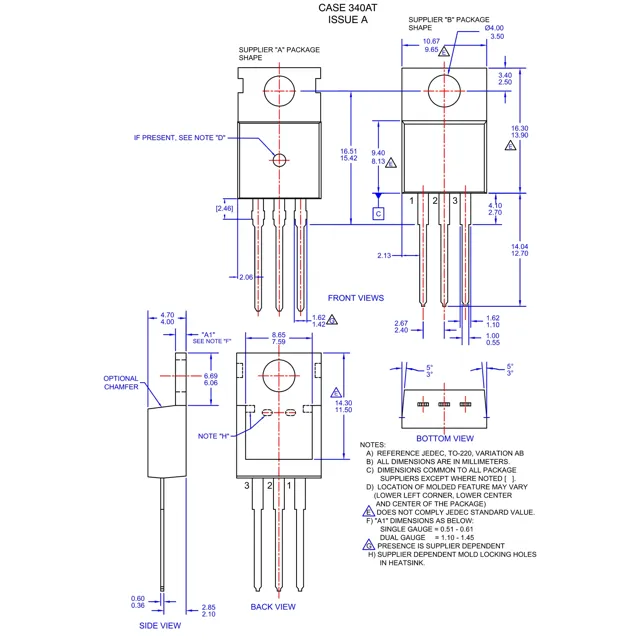
TO-220-3
Description:
N-Channel Tube 360mOhm @ 6.5A, 10V ±20V 1143 pF @ 400 V 25.3 nC @ 10 V 800 V TO-220-3
Quantity:
Unit Price: $3.265901
Ext Price: $3.27
Delivery:


Payment:


In Stock : 273
Minimum: 1 Multiples: 1
Qty
Unit Price
Ext Price
1
$3.265901
$3.27
10
$3.081039
$30.81
100
$2.906640
$290.66
500
$2.742113
$1,371.06
1000
$2.586899
$2,586.90
Want a lower wholesale price? Please send RFQ, we will respond immediately.
RFQ Now
Add to RFQ list
You may place an order without registering to Utmel.
We strongly suggest you sign in before purchasing as you can track your order in real time.
For your convenience, we accept multiple payment methods in USD, including PayPal, Credit Card, and wire transfer.
RFQ (Request for Quotations)It is recommended to request for quotations to get the latest prices and inventories about the part.
Our sales will reply to your request by email within 24 hours.
1. You'll receive an order information email in your inbox. (Please remember to check the spam folder if you didn't hear from us).
2. Since inventories and prices may fluctuate to some extent, the sales manager is going to reconfirm the order and let you know if there are any updates.
- TypeParameter
- Mounting Type
The "Mounting Type" in electronic components refers to the method used to attach or connect a component to a circuit board or other substrate, such as through-hole, surface-mount, or panel mount.
Through Hole - Package / Case
refers to the protective housing that encases an electronic component, providing mechanical support, electrical connections, and thermal management.
TO-220-3 - Supplier Device Package
The parameter "Supplier Device Package" in electronic components refers to the physical packaging or housing of the component as provided by the supplier. It specifies the form factor, dimensions, and layout of the component, which are crucial for compatibility and integration into electronic circuits and systems. The supplier device package information typically includes details such as the package type (e.g., DIP, SOP, QFN), number of pins, pitch, and overall size, allowing engineers and designers to select the appropriate component for their specific application requirements. Understanding the supplier device package is essential for proper component selection, placement, and soldering during the manufacturing process to ensure optimal performance and reliability of the electronic system.
TO-220-3 - Mfronsemi
- PackageTube
- Product StatusActive
- Current - Continuous Drain (Id) @ 25℃13A (Tc)
- Drive Voltage (Max Rds On, Min Rds On)10V
- Power Dissipation (Max)96W (Tc)
- Base Product Number
"Base Product Number" (BPN) refers to the fundamental identifier assigned to a component by the manufacturer. This number is used to identify a specific product family or series of components that share common features, characteristics, or functionality. The BPN is usually part of a larger part number or order code that includes additional information, such as variations in packaging, tolerance, voltage ratings, and other specifications.
NTP360 - Continuous Drain Current Id13
- Number of Elements per Chip1
- Package TypeTO-220
- Channel ModeEnhancement
- Vds - Drain-Source Breakdown Voltage800 V
- Vgs th - Gate-Source Threshold Voltage3.8 V
- Pd - Power Dissipation96 W
- Transistor PolarityN-Channel
- Maximum Operating Temperature
the maximum body temperature at which the thermistor is designed to operate for extended periods of time with acceptable stability of its electrical characteristics.
+ 150 C - Vgs - Gate-Source Voltage- 20 V, + 20 V
- Minimum Operating Temperature- 55 C
- Factory Pack QuantityFactory Pack Quantity50
- Mounting StylesThrough Hole
- Manufactureronsemi
- Brandonsemi
- Qg - Gate Charge25.3 nC
- Rds On - Drain-Source Resistance360 mOhms
- RoHSDetails
- Id - Continuous Drain Current13 A
- MSLMSL 1 - Unlimited
- Qualification-
- Operating Temperature
The operating temperature is the range of ambient temperature within which a power supply, or any other electrical equipment, operate in. This ranges from a minimum operating temperature, to a peak or maximum operating temperature, outside which, the power supply may fail.
-55°C ~ 150°C (TJ) - Packaging
Semiconductor package is a carrier / shell used to contain and cover one or more semiconductor components or integrated circuits. The material of the shell can be metal, plastic, glass or ceramic.
Tube - SubcategoryMOSFETs
- Pin Count
a count of all of the component leads (or pins)
3 - Number of Channels1 Channel
- Power Dissipation
the process by which an electronic or electrical device produces heat (energy loss or waste) as an undesirable derivative of its primary action.
96 - FET Type
"FET Type" refers to the type of Field-Effect Transistor (FET) being used in an electronic component. FETs are three-terminal semiconductor devices that can be classified into different types based on their construction and operation. The main types of FETs include Metal-Oxide-Semiconductor FETs (MOSFETs), Junction FETs (JFETs), and Insulated-Gate Bipolar Transistors (IGBTs).Each type of FET has its own unique characteristics and applications. MOSFETs are commonly used in digital circuits due to their high input impedance and low power consumption. JFETs are often used in low-noise amplifiers and switching circuits. IGBTs combine the high input impedance of MOSFETs with the high current-carrying capability of bipolar transistors, making them suitable for high-power applications like motor control and power inverters.When selecting an electronic component, understanding the FET type is crucial as it determines the device's performance and suitability for a specific application. It is important to consider factors such as voltage ratings, current handling capabilities, switching speeds, and power dissipation when choosing the right FET type for a particular circuit design.
N-Channel - Rds On (Max) @ Id, Vgs
Rds On (Max) @ Id, Vgs refers to the maximum on-resistance of a MOSFET or similar transistor when it is fully turned on or in the saturation region. It is specified at a given drain current (Id) and gate-source voltage (Vgs). This parameter indicates how much resistance the component will offer when conducting, impacting power loss and efficiency in a circuit. Lower Rds On values are preferred for better performance in switching applications.
360mOhm @ 6.5A, 10V - Vgs(th) (Max) @ Id
The parameter "Vgs(th) (Max) @ Id" in electronic components refers to the maximum gate-source threshold voltage at a specified drain current (Id). This parameter is commonly found in field-effect transistors (FETs) and is used to define the minimum voltage required at the gate terminal to turn on the transistor and allow current to flow from the drain to the source. The maximum value indicates the upper limit of this threshold voltage under specified operating conditions. It is an important parameter for determining the proper biasing and operating conditions of the FET in a circuit to ensure proper functionality and performance.
3.8V @ 300μA - Input Capacitance (Ciss) (Max) @ Vds
The parameter "Input Capacitance (Ciss) (Max) @ Vds" in electronic components refers to the maximum input capacitance measured at a specific drain-source voltage (Vds). Input capacitance is a crucial parameter in field-effect transistors (FETs) and power MOSFETs, as it represents the total capacitance at the input terminal of the device. This capacitance affects the device's switching speed and overall performance, as it influences the time required for charging and discharging during operation. Manufacturers provide this parameter to help designers understand the device's input characteristics and make informed decisions when integrating it into a circuit.
1143 pF @ 400 V - Gate Charge (Qg) (Max) @ Vgs
Gate Charge (Qg) (Max) @ Vgs refers to the maximum amount of charge that must be supplied to the gate of a MOSFET or similar device to fully turn it on, measured at a specific gate-source voltage (Vgs). This parameter is crucial for understanding the switching characteristics of the device, as it influences the speed at which the gate can charge and discharge. A higher gate charge value often implies slower switching speeds, which can impact the efficiency of high-frequency applications. This parameter is typically specified in nanocoulombs (nC) in the component's datasheet.
25.3 nC @ 10 V - Drain to Source Voltage (Vdss)
The Drain to Source Voltage (Vdss) is a key parameter in electronic components, particularly in field-effect transistors (FETs) such as MOSFETs. It refers to the maximum voltage that can be applied between the drain and source terminals of the FET without causing damage to the component. Exceeding this voltage limit can lead to breakdown and potentially permanent damage to the device.Vdss is an important specification to consider when designing or selecting components for a circuit, as it determines the operating range and reliability of the FET. It is crucial to ensure that the Vdss rating of the component is higher than the maximum voltage expected in the circuit to prevent failures and ensure proper functionality.In summary, the Drain to Source Voltage (Vdss) is a critical parameter that defines the maximum voltage tolerance of a FET component and plays a significant role in determining the overall performance and reliability of electronic circuits.
800 V - Vgs (Max)
Vgs (Max) refers to the maximum gate-source voltage that can be applied to a field-effect transistor (FET) without causing damage to the component. This parameter is crucial in determining the safe operating limits of the FET and helps prevent overvoltage conditions that could lead to device failure. Exceeding the specified Vgs (Max) rating can result in breakdown of the gate oxide layer, leading to permanent damage to the FET. Designers must ensure that the applied gate-source voltage does not exceed the maximum rating to ensure reliable and long-term operation of the electronic component.
±20V - Product Type
a group of products which fulfill a similar need for a market segment or market as a whole.
MOSFET - Channel Type
In electronic components, the parameter "Channel Type" refers to the type of channel through which electrical signals or current flow within the component. This parameter is commonly associated with field-effect transistors (FETs) and other semiconductor devices. The channel type can be categorized as either N-channel or P-channel, depending on the polarity of the majority charge carriers (electrons or holes) that carry the current within the channel. N-channel devices have an electron-conducting channel, while P-channel devices have a hole-conducting channel. Understanding the channel type is crucial for proper circuit design and component selection to ensure compatibility and optimal performance.
N - FET Feature
FET Feature refers to the specific characteristics or attributes of a Field-Effect Transistor (FET) that distinguish it from other types of transistors. FETs are semiconductor devices commonly used in electronic circuits for amplification or switching purposes. Some common features of FETs include high input impedance, low output impedance, and voltage-controlled operation. These features make FETs suitable for various applications where precise control of current and voltage is required. Understanding the FET features is essential for selecting the right transistor for a particular circuit design and ensuring optimal performance.
- - Product Category
a particular group of related products.
MOSFET


