

 Product
 Brand
Brand Articles
 Tools
Tools
Switch Debouncing for MCU Inputs: RC, Schmitt Trigger, or Firmware?
A switch debounce circuit (or equivalent firmware routine) prevents the elastic rebound of mechanical switch contacts from generating multiple false logic transitions on a microcontroller (MCU) input. Choosing the right conditioning method comes down to how your MCU reads the pin and what input structure sits behind the pad: firmware debouncing eliminates external passive and active components when a background hardware timer can periodically sample the pin[5], a passive RC low-pass filter absorbs rapid contact spikes into an exponential analog voltage slope[7], and adding a Schmitt trigger restores fast, noise-immune digital edges required by asynchronous interrupts, clock inputs, and standard CMOS logic gates[2].
Instead of comparing disconnected schematic fragments, this guide benchmarks all three methods on one unified reference circuit: a standard two-terminal single-pole single-throw (SPST) push button wired in an active-low configuration.
The Unified Reference Scenario (Active-Low SPST Input)
Throughout every schematic analysis, firmware architecture, and oscilloscope capture below, we evaluate the exact same electrical node:
Switch Topology: A two-terminal SPST mechanical contact connected between the MCU digital input pin (GPIO / External Interrupt
EXTI) and ground ().Baseline Pull-Up (): A pull-up resistor connected between the MCU input node and the positive supply rail (, evaluated ator). When the switch is open (idle),holds the MCU pin at logic
HIGH(). When the button is pressed, the contacts close to, pulling the node to logicLOW().Active-High Contrast: Reversing this position—placing the switch betweenand the MCU pin with a resistor to—creates an active-high configuration that idles atand assertswhen pressed. If you are deciding how to bias your baseline input node for noise immunity or current leakage, review the foundational differences between pull-up and pull-down resistors.
Bench Pull-Up Nuance (vs. Internal): While textbook diagrams routinely assume aexternal resistor, enabling a microcontroller's internal pull-up (
INPUT_PULLUP) introduces a much weaker resistance—often specified broadly betweenand. In a documented bench test case, measuring an Arduino Nano Every pin (D2configured asINPUT_PULLUP) yielded an actual internal resistance of . To mirror real-world MCU behavior, the documented hardware bench captures below use a pull-up resistor, which significantly stretches capacitor recharge times if you add external RC filtering.
Decision Framework & Comparison: RC Filter vs. Schmitt Trigger vs. Firmware
Selecting between hardware and software debouncing depends on three circuit constraints: whether the MCU input is polled by a timer or driven by an edge interrupt, whether the GPIO buffer integrates internal hysteresis, and whether PCB footprint or CPU timer management is the tighter project constraint.
3-Step Engineering Decision Workflow
Evaluate your target MCU pin against these three questions before adding components to your schematic:
How does the MCU acquire the input signal?
YES — Polled periodically by a background system tick timer: Use Firmware Debouncing. You already have a periodic timebase, so external RC components only add BOM lines and board area.
NO — Wired to an asynchronous external interrupt (
EXTI), deep-sleep wake-up pin, or hardware counter/flip-flop clock: Move to step 2. Raw contact bounce on an edge-triggered line will flood the interrupt service routine (ISR) or falsely clock sequential logic[8].Does the target MCU GPIO pin include built-in Schmitt-trigger hysteresis?
YES — Datasheet confirms sufficient input hysteresis () and tolerates slow input edges: A Passive RC Filter (with a current-limiting series resistor) can smooth the contact bounce directly before the MCU pin.
NO — Input is a standard CMOS buffer with strict maximum rise/fall transition-rate () limits: Pair your RC filter with an external Schmitt Trigger IC to prevent dynamic shoot-through current and logic oscillation during slow capacitor ramps.
Can your firmware disable the pin interrupt upon the first edge and hand off to a hardware timer?
YES — A spare timer or non-blocking tick is available: You can implement an ISR Lockout Firmware Pattern without external hardware.
NO — The signal must arrive at the pin as a single, clean digital transition: Use an RC + Schmitt Trigger hardware circuit.
Key Specifications & Architectural Comparison Matrix
The table below compares all three conditioning strategies applied to our baseline active-low SPST switch node:
| Evaluation Parameter | Option 1: Passive RC Filter | Option 2: RC + Schmitt Trigger | Option 3: Firmware Debouncing |
|---|---|---|---|
| Signal Waveform at MCU Pin | Exponential analog charge/discharge slope (with stepped plateaus during contact rebound) | Crisp, rail-to-rail digital square edge (e.g.,transition on bench) | Raw, jagged rail-to-rail contact bounce spikes () |
| External Hardware Needed | 1–2 resistors + 1 capacitor (+ optional steering diode) | RC network + Schmitt trigger buffer/inverter IC (or single-gate package) | None beyond baseline pull-up/pull-down resistor (often internal to MCU) |
| Suitability for Raw Edge Interrupts (EXTI) | Conditional (only if MCU pin integrates true Schmitt hysteresis) | High (delivers a single clean digital edge per press and release) | Low unless ISR immediately disables the pin interrupt during a lockout window |
| CMOS Slow-Transition Risk | High on standard CMOS inputs lacking hysteresis | Eliminated via dual thresholds (and) | None (voltage transitions remain fast, though noisy) |
| CPU / Timer Overhead | Zero | Zero | Requires periodic timer polling or ISR lockout timer management |
| Primary Strength / Best For | Low-part-count noise smoothing into MCU pins with verified internal hysteresis | Asynchronous interrupt lines, wake-up pins, and non-MCU sequential logic | Cost- and space-constrained PCBs running an active system tick timer |
| Primary Drawback | Slow rise/fall ramps risk internal oscillation on standard CMOS gates | Adds active IC footprint, BOM lines, and potential logic polarity inversion | Naive blocking delays stall the CPU; unprotected edge ISRs cause interrupt storms |
Application Boundaries: Who Should NOT Choose Each Option
Do NOT choose a bare Passive RC Filter if: Your switch feeds a standard CMOS logic gate, a flip-flop clock line, or an MCU GPIO lacking internal hysteresis. A slow RC voltage ramp lingering near the logic threshold violates CMOS transition-rate specifications, causing both PMOS and NMOS input transistors to conduct simultaneously.
Do NOT choose an External Schmitt Trigger IC if: Your microcontroller already provides Schmitt-trigger inputs on its GPIO ports and runs a periodic background timer (such as
SysTick) that can sample button states in software at zero hardware cost.Do NOT choose Firmware-Only Debouncing if: The switch directly clocks discrete digital logic or wakes an MCU from a deep-sleep state where high-frequency contact bounce triggers repeated wake/sleep cycles before software timers initialize.
Category Boundary — Why SR Latch Debouncing Is Excluded: Textbooks frequently present Set-Reset (SR) latches alongside RC filters, but as Jack Ganssle notes, an SR latch debounce circuit requires a three-terminal double-throw (SPDT) switch that alternately pulls one of two inputs to ground. Because standard tactile push buttons are two-terminal SPST devices, SR latch debouncing cannot be applied to our baseline circuit without changing the mechanical switch itself.
Why Mechanical Contact Bounce Causes False MCU Triggers (Thresholds & Real Data)
When metal switch contacts close or release, elastic momentum and surface microscopic roughness cause them to rebound open and closed repeatedly before settling. Because a digital microcontroller input evaluates voltage continuously in the nanosecond domain, every time the bouncing voltage crosses the input buffer's logic high () and logic low () thresholds, the MCU registers a separate button press or release.
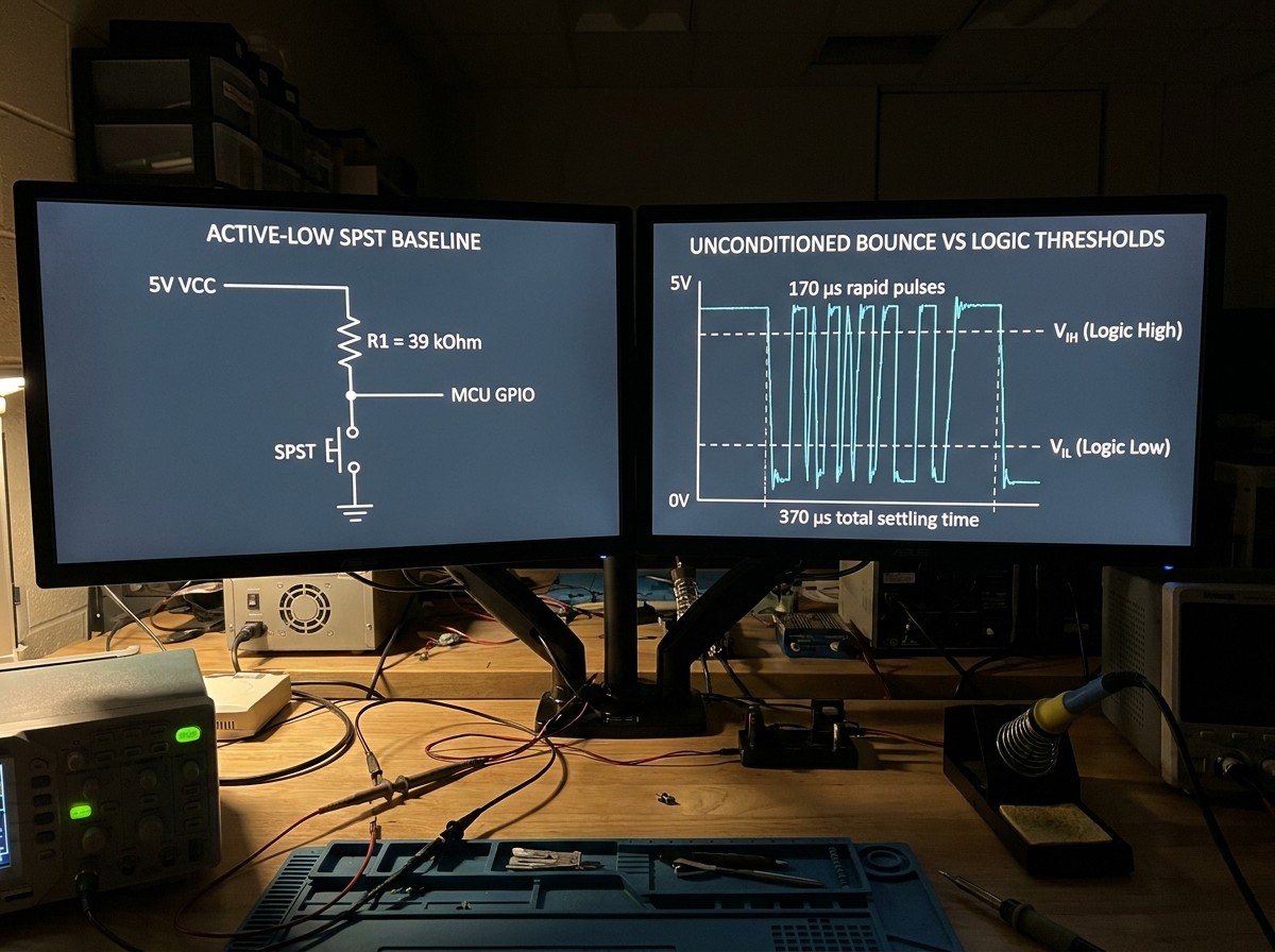
Pull-Up/Pull-Down Baseline andThreshold Crossings
In our active-low reference circuit, pull-up resistorholds the open switch node at(), safely above the MCU's minimum high-level input voltage (). The moment the button is pressed and the moving wiper first touches the stationary ground contact, the node voltage drops rapidly to(below the maximum low-level input voltage,).
However, when the contacts elastically rebound apart a few microseconds later, the path to ground opens and pull-up resistorimmediately yanks the node back toward. When the contacts strike again, the voltage plunges back to. Instead of a single falling edge fromto, the MCU pin sees a high-speed train of rail-to-rail square pulses crossing back and forth acrossand.
Bench Tip — Measuring Your MCU's True Internal Pull-Up Resistance:
Before calculating how quickly an input node recharges or how it interacts with an external capacitor, you need to know the real resistance of your pull-up path. Microcontroller datasheets typically list wide process-variation windows (such asto) for internal pull-ups. You can measure the exact value on your bench in three steps:
Configure the target GPIO pin as
INPUT_PULLUPand measure its open-circuit output voltage with a digital multimeter (on our Arduino Nano Every PinD2, this measured ).Connect a variable resistor (potentiometer) between that GPIO pin and, then adjust the dial until the pin voltage drops to exactly half of the open-circuit reading ( on the bench), forming a 1:1 resistive voltage divider with the internal pull-up.
Disconnect the potentiometer from the circuit and measure its resistance across the active terminals. Our multimeter read —confirming why adiscrete pull-up resistor models internal MCU pull-up behavior far more accurately than a textbookpart.
Empirical Bounce Duration Reality Check: Ganssle's Data vs. Switch Aging
A common myth repeated in introductory tutorials is that mechanical switches always bounce for a fixed "10 to 20 milliseconds." Empirical laboratory testing proves that bounce duration is far more variable—and usually much shorter on healthy switches, though subject to severe outliers.
In Jack Ganssle's empirical study (hosted by the University of Utah), he tested 18 different mechanical switches, actuating each switch 300 times on asupply with apull-up resistor:
Bounce occurred "sometimes a lot, sometimes not at all."
Across 16 of the 18 switches, the average bounce duration was()[1], and the maximum recorded bounce was().
Only two outlier switches in the entire test set exceeded—one reachedon closure, and one battered switch reachedon opening.
In the documented oscilloscope bench test case, a mechanical contact closure wired with apull-up togenerated violent rail-to-rail (to) square pulses for the first , followed by high-frequency analog ringing that settled completely after .
Why, then, can you not simply hard-code afilter for every product? As Analog Devices documents, mechanical switch bounce is not consistent from unit to unit, across manufacturing lots, or over the operating lifespan[6] of an individual switch. As metal contacts oxidize, pit, or lose spring tension over thousands of actuations, both contact resistance and bounce duration shift—meaning your RC time constant or firmware timer must include a generous engineering safety margin beyond what a single brand-new switch shows on the bench.
Option 1 — Passive RC Switch Debounce Circuit (Time Constant & Charge/Discharge Paths)
A passive RC switch debounce circuit places a resistor-capacitor low-pass network between the mechanical contact and the MCU input so the capacitor absorbs rapid bounce spikes and forces the node voltage to change exponentially according to the time constant. While inexpensive, bare RC networks suffer from press/release asymmetry and create slow analog slopes that can destabilize standard CMOS inputs.
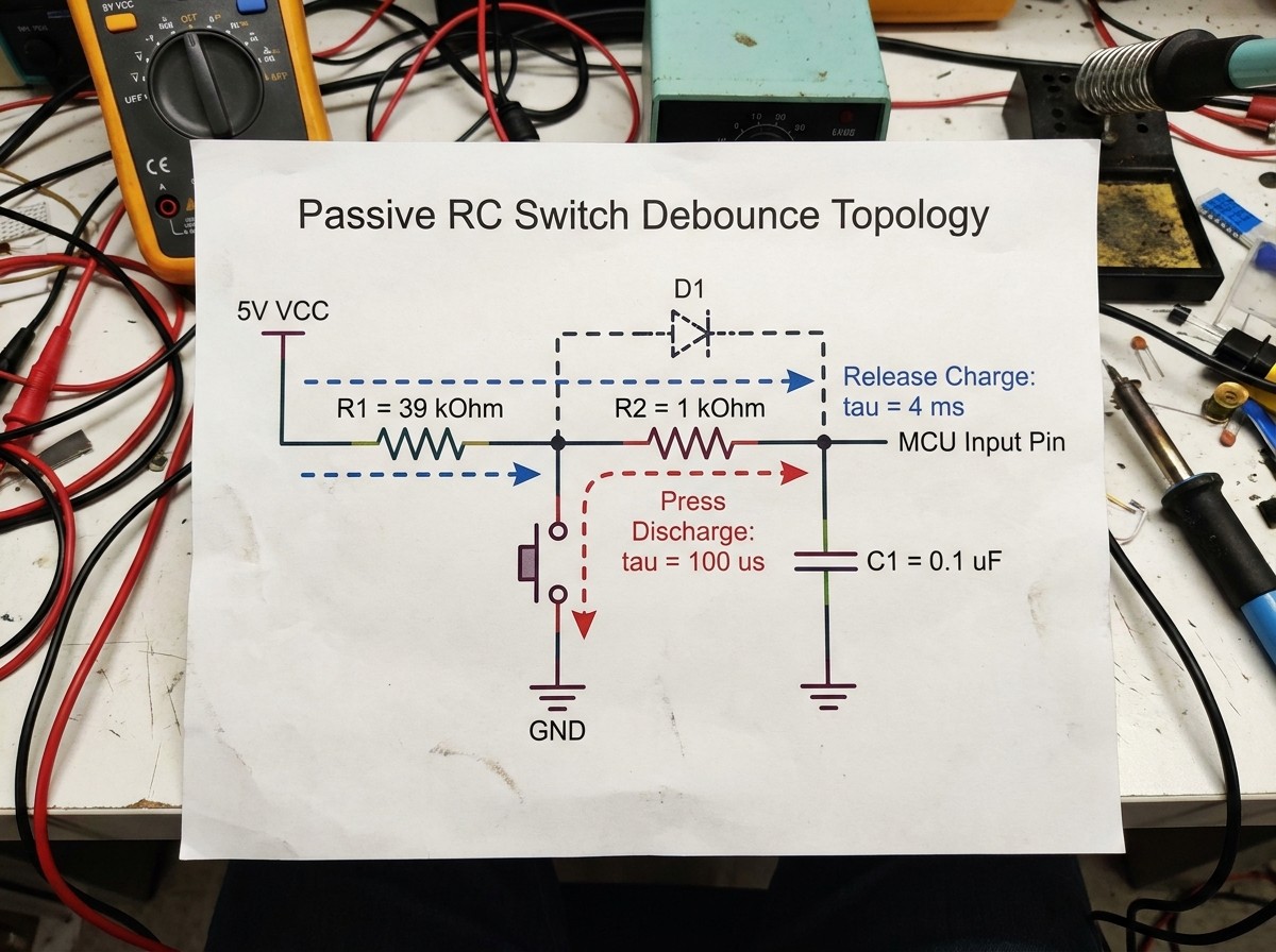
Calculating the RC Time Constant () on the Active-Low Input
To filter our active-low SPST switch without shorting a charged capacitor directly across the metal contacts, we add a series resistorbetween the pull-up/switch junction and the MCU input pin, and place capacitorfrom the MCU input pin to:
When the switch is open (releasing the button): Capacitorcharges towardthrough the series combination of.
When the switch closes (pressing the button): The junction betweenandis pulled to, and capacitordischarges toexclusively through.
Per Pico Technology, the RC time constant (, within Ohms andin Farads) defines the time required for a discharging capacitor's voltage to decay to roughly $37\%$ () of its initial voltage[7]—or rise to roughly $63\%$ ofwhen charging.
Illustrative Bench Calculation Example:
(Note: The component values below are illustrative bench examples to demonstrate the math; always tuneandto your measured switch bounce and MCU threshold specifications.)
Suppose an engineer prototypes a textbook external network usingand:
Now consider our realistic bench circuit using a pull-up (), a series resistor (), and a capacitor ():
On Button Press (Discharge through):.
On Button Release (Charge through):.
If contacts momentarily bounce open for a few dozen microseconds during a press,must recharge through the largepath (), preventing the node voltage from climbing back across the MCU'sthreshold before the contacts close again.
Press vs. Release Asymmetry and the Steering Diode () Refinement
Notice the side effect of naive RC circuits:
The Bare Capacitor Mistake (Omitting): If a hobbyist wires acapacitor directly in parallel with the switch contacts (no series resistor), pressing the button shorts the fully charged capacitor directly through the mechanical contacts. This creates a sharp current spike that pits the switch contacts over time, and leaves zero resistance () to control the discharge slope.
Independent Charge/Discharge Control via Steering Diode: When both button press and button release edges need independently controlled time constants, engineers place a steering diode () in parallel with resistor. Depending on the diode's orientation, charging current can bypass(flowing only throughandwhen the switch is open) while discharge current is forced throughwhen the switch closes—or vice versa—allowing you to decouple press filtering from release recovery.
The Hidden Trap of Bare RC Filters: Stepped Decay and CMOS Oscillation
When probing the output of the passive RC network (,,) on a GW Instek MDO-2204EG oscilloscope in this documented bench test during aswitch closure, the sharp rail-to-rail spikes disappeared—but two critical real-world phenomena emerged:
Stepped Analog Decay: The voltage took over to fall fromto. Instead of a smooth textbook curve, the trace displayed distinct horizontal "steps" and slight upward bumps mid-slope. Each step marks the exact microsecond the mechanical contacts bounced open during the transition, briefly halting the discharge throughwhiletried to pull the capacitor back up.
CMOS Input Oscillation and Shoot-Through Current: Feeding a(or multi-millisecond) stepped slope directly into a standard digital input is hazardous. As documented in Texas Instruments Application Report SLLA364A, standard CMOS logic inputs require fast input transition rates (). When a slowly moving RC voltage lingers in the intermediate region betweenand, both the top PMOS and bottom NMOS transistors in the input stage conduct simultaneously[2]. This creates a low-impedance shoot-through path fromto, resulting in excessive surge current, supply/ground bounce, and wild output oscillations where the MCU or logic gate toggles rapidly between HIGH and LOW during a single transition.
Option 2 — RC Filter + Schmitt Trigger Hysteresis (Solving Slow-Edge Risks)
Placing a Schmitt trigger buffer or inverter between the passive RC filter and the microcontroller input eliminates CMOS transition-rate failures by enforcing dual switching thresholds: a positive-going threshold () and a negative-going threshold () separated by a hysteresis voltage band (). Once the slow RC curve crosses the active threshold, internal positive feedback snaps the output into a single, nanosecond-scale digital edge.
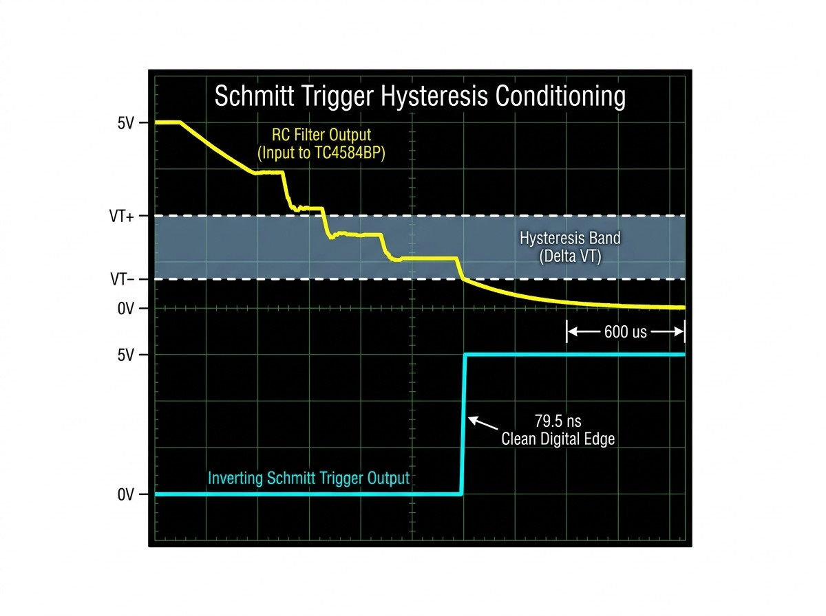
How Hysteresis (and) Shields the MCU from Intermediate Glitches
Unlike a standard CMOS gate that switches around a single narrow threshold region—making any noise ripple or RC bounce plateau near that voltage trigger multiple output toggles—a Schmitt trigger splits the switching point into two distinct voltage levels.
According to Texas Instruments Application Brief SCEA046B, Schmitt-trigger inputs operate across defined threshold windows:
Rising Input Threshold (): A rising signal must climb betweenand(where) before the input recognizes a logic HIGH.
Falling Input Threshold (): A falling signal must drop betweenand(where) before the input recognizes a logic LOW.
Hysteresis Band (): In standard TI Schmitt-trigger logic families, this hysteresis buffer window typically spanstoatandtoat[3].
When our active-low button is pressed and the RC capacitor discharges downward, the Schmitt trigger output remains locked until the voltage drops all the way past. If the switch contacts bounce open right after crossing, causing a stepped plateau or small upward glitch on the capacitor waveform, nothing happens at the output as long as that upward ripple does not climb all the way back across the upper threshold. For a deeper look at how internal comparator feedback creates this dual-threshold transfer curve, see our engineering guide on what is a Schmitt trigger.
Verified Hardware Examples & Bench Waveform Result:
Bench Test with Toshiba TC4584BP (Hex Inverting Schmitt Trigger): In the documented bench test, feeding thestepped RC decay (supply) into the input of a TC4584BP Schmitt trigger IC and measuring the output with oscilloscope cursors showed the sluggish analog slope transformed into a single, razor-sharp digital edge with a measured transition time of —matching the Toshiba datasheet's typicaltransition specification at.
Sequential Logic with Integrated Schmitt Inputs (TI SN74HCS74): If your switch directly clocks a hardware flip-flop or toggle circuit rather than an MCU pin, selecting a device with built-in Schmitt-trigger inputs—such as the Texas Instruments SN74HCS74 Dual D-Type Positive-Edge-Triggered Flip-Flop (tooperation,typical quiescent current)[4]—allows the chip to accept slow RC debounce transitions directly on its clock and data pins without an external buffer IC.
Two Practical Hardware Details: Logic Inversion and Internal MCU Hysteresis
Before placing a Schmitt trigger IC on your PCB, check two details that frequently trip up embedded designs:
The Inverting Gate Polarity "Gotcha": Many common Schmitt trigger ICs used in debounce schematics (including hex inverters like the
TC4584BPor single-gate inverting buffers) are inverting logic gates—indicated by the negation bubble on the schematic symbol. In our baseline active-low circuit, the switch node idles at(HIGH) and drops to(LOW) when pressed. Passing that signal through a single inverting Schmitt trigger stage flips the logic polarity: the MCU pin now idles at (LOW) and snaps to (HIGH) when the button is pressed. You must either configure your MCU interrupt/polling code for an active-high (RISINGedge) press, cascade two inverter stages, or select a non-inverting Schmitt buffer.Check Your MCU Datasheet Before Buying an External IC: As practitioners on the EEVblog forum emphasize, many modern 8-bit and 32-bit microcontrollers already integrate Schmitt-trigger hysteresis into their digital GPIO input buffers. Open your MCU datasheet's I/O Port Characteristics table and look for the input hysteresis parameter (). If your MCU pin already provides a true Schmitt-trigger input with sufficient hysteresis to mask your RC steps, an external Schmitt trigger IC is redundant.
Option 3 — Firmware Debouncing on the Same Input (Polling, Timers, and Interrupt Lockouts)
Firmware debouncing connects our active-low SPST switch and pull-up resistor directly to the MCU GPIO pin—using zero capacitors or external ICs—and filters out contact bounce in software by verifying that the pin state remains stable over a time window. To work reliably in production systems, the firmware architecture must avoid blocking the processor and prevent raw edge-interrupt floods.
Patterns 1 & 2: Naive Blocking Delays vs. Periodic Timer Sampling
When an unconditioned active-low switch is pressed, the MCU pin oscillates rapidly between HIGH and LOW for hundreds of microseconds to several milliseconds. Software can filter this noise using two polling techniques:
Pattern 1 — Naive Blocking Wait (
delay()): The main loop detects that the pin readsLOW, executes a hard-coded blocking wait to let the contacts settle, and reads the pin a second time to confirm it is stillLOW. While simple for beginner demos, stalling the CPU for several milliseconds inside a main loop starves communication buffers, display refreshes, and control loops.Pattern 2 — Periodic Timer Polling (Non-Blocking Shift/Counter Filter): A hardware timer (such as
SysTickor a general-purpose peripheral timer) fires at a regular background interval. Each time the timer ticks, it reads the raw GPIO level and shifts the bit into an integer variable or increments a stability counter. Any contact bounce during the transition resets the sequence. The firmware registers a valid button press only after the pin readsLOWacrossconsecutive timer samples whose total duration exceeds the switch's worst-case bounce window.
Pattern 3: Preventing External Interrupt (EXTI) Storms via ISR Lockout
What happens if you attach an asynchronous falling-edge external interrupt (EXTI) directly to our unconditioned active-low button? During a single press, everytocontact rebound crosses the threshold and re-triggers the hardware interrupt controller—flooding the CPU with back-to-back ISR context switches and potentially corrupting state variables.
As detailed in the Infineon Developer Community, you can safely debounce an interrupt-driven pin without external hardware by using an ISR Lockout + Timer Handoff pattern:
Disable the Pin Interrupt Immediately: On the very first falling edge, the GPIO ISR immediately masks/disables further state-change interrupts on that pin so subsequent bounce edges are ignored by hardware.
Start a Non-Blocking Debounce Timer: The ISR starts a small one-shot hardware timer (or records a timestamp) configured for your debounce lockout period.
Re-Sample and Re-Enable on Timer Expiry: When the timer interrupt fires after the bounce window has elapsed, the timer ISR reads the GPIO pin to verify the button is genuinely held
LOW, dispatches the button event, and re-enables the pin state-change interrupt for the next action.
#include <stdint.h> #include <stdbool.h>
// Set lockout ticks to exceed measured worst-case switch bounce + aging margin // (e.g., if timer ticks every 1 ms, 10 ticks = 10 ms lockout window) #define DEBOUNCE_LOCKOUT_TICKS 10U
static volatile bool g_lockout_active = false; static volatile uint16_t g_lockout_counter = 0U; static volatile bool g_button_pressed_event = false;
// 1. External Pin Interrupt (Falling Edge on Active-Low SPST Switch) void EXTI_Button_ISR(void) { if (!g_lockout_active) { MCU_DisablePinInterrupt(BUTTON_PIN); // Stop ISR storm during bounce g_lockout_active = true; g_lockout_counter = DEBOUNCE_LOCKOUT_TICKS; } }
// 2. Periodic Background Hardware Timer ISR (Non-Blocking) void Timer_Tick_ISR(void) { if (g_lockout_active) { if (g_lockout_counter > 0U) { g_lockout_counter--; } else { // Lockout window expired: sample stabilized active-low pin if (MCU_ReadPin(BUTTON_PIN) == 0U) { g_button_pressed_event = true; } g_lockout_active = false; MCU_ClearPendingPinInterrupt(BUTTON_PIN); MCU_EnablePinInterrupt(BUTTON_PIN); // Re-arm for next press } } }
How to Capture and Compare Switch Bounce Waveforms on an Oscilloscope
Because mechanical contact bounce is a fast, non-repeating one-shot transient, capturing it on a digital storage oscilloscope (DSO) requires switching out of Auto sweep and arming Single trigger mode with the trigger threshold positioned inside the logic transition window. Probing all three stages of our reference circuit reveals exactly how the signal transforms from jagged spikes to an exponential slope to a 79.5-nanosecond square edge.
Switch De-Bounce Using Schmitt
Step-by-Step Oscilloscope Setup (Single Trigger Procedure)
If you leave an oscilloscope in Auto trigger mode and press a push button, the trace will flash across the screen and immediately get overwritten by a flat line. Follow this bench procedure to freeze the bounce event:
Connect the Probe: Attach the oscilloscope probe ground clip to circuitand hook the probe tip to the active-low switch node (or the output of the RC / Schmitt stage under test).
Set Vertical & Horizontal Scales: Adjust the vertical scale toorso the fullto(or) transition fills the display. Set the initial horizontal timebase betweenandto view the full settling envelope, then zoom in towhen measuring Schmitt trigger edge speeds.
Configure Edge & Threshold Level: Select Edge Trigger mode. For an active-low button press (high-to-low transition), select a Falling Edge slope (or Rising Edge if probing after an inverting Schmitt trigger). Position the trigger voltage level near the midpoint of(e.g.,on arail) so the scope triggers on the very first downward contact strike.
Arm
SingleCapture Mode: Press theSinglebutton on the oscilloscope. The scope will wait in aReady/Armedstate until you actuate the switch, capture that single transition into memory, and freeze the display for cursor inspection.Bench Stress-Test Tip (Using a Relay for Repeatable Bounce): Modern miniature tactile buttons sometimes exhibit very little bounce under a gentle finger press, making it frustrating to tune filters on command. On our test bench, wiring a programmable timer relay module (cycling once per second) in place of the button produced heavy, repeatable mechanical contact bounce on every single cycle—ideal for stress-testing RC and Schmitt trigger stages hands-free.
Side-by-Side Oscilloscope Waveform Comparison (3 Probe Points)
The table below synthesizes the actual oscilloscope captures recorded across the three probe points of ouractive-low reference circuit on a GW Instek MDO-2204EG oscilloscope:
| Probe Point on Reference Circuit | Observed Oscilloscope Waveform Shape | Measured Settling / Transition Behavior (Bench Data) | How the Downstream MCU Input Buffer Reacts |
|---|---|---|---|
| 1. Raw Unconditioned Switch Node (pull-up to) | Violent rail-to-rail square pulses () followed by high-frequency analog noise/ringing | of rail-to-rail pulses; total settling time (up toacross 16 of 18 switches in Ganssle's study) | Registers multiple false presses and ISR triggers as the signal crossesandrepeatedly |
| 2. Passive RC Filter Output (pull-up +series +cap) | Drawn-out exponential decay curve featuring distinct horizontal "steps" where contacts briefly reopened mid-discharge | slow fall time fromto(discharges toof initial voltage) | Elimates sharp spikes, but risks shoot-through current and oscillation on standard CMOS inputs lacking hysteresis |
| 3. RC + Inverting Schmitt Trigger Output (Toshiba TC4584BP / TI SN74HCS74) | Single, clean digital step (inverted fromLOW toHIGH on press through the inverting gate) | measured transition time (matchingdatasheet typical spec at) once RC voltage crosses | Registers a single, noise-free logic transition safe for asynchronous interrupts and clock inputs |
Why Engineering Sources and AI Summaries Disagree (Mistakes & Verification Checklist)
If you search for switch debouncing advice, you will find sharp disagreement: some guides insist an RC filter plus a Schmitt trigger IC is mandatory for every button, while embedded veterans argue hardware debounce circuits are an unnecessary waste of board space. Both camps are right within their respective domains—and wrong when their advice is applied universally.
Resolving the Conflict: Firmware-First vs. Hardware Signal-Integrity Camps
Why Embedded Firmware Veterans Reject Hardware RC Circuits: In A Guide to Debouncing, Jack Ganssle argues that when a microcontroller already runs a periodic timer interrupt, debouncing buttons in software costs zero cents, consumes zero PCB area, and avoids component tolerance drift. For polled user-interface buttons connected to standard MCU GPIOs, adding external resistors, capacitors, and Schmitt ICs is unnecessary hardware overhead.
Why Semiconductor & Hardware Guides Insist on RC + Schmitt Conditioning: Conversely, documentation from Texas Instruments and DigiKey addresses signal integrity at the silicon boundary. When a switch feeds discrete sequential logic (where no MCU exists), drives an asynchronous wake-up line while the MCU is asleep, or uses a passive RC network connected to a standard CMOS input with strictlimits, hardware conditioning with Schmitt-trigger hysteresis is mandatory to prevent false clocking and shoot-through current.
Why "Just Slap a 104 () Capacitor Across the Button" Is Dangerous Advice: Casual hobbyist posts often advise soldering a bareceramic capacitor directly across push-button legs. As shown in our bench analysis, this shorts the capacitor through the switch contacts on closure (causing high peak discharge currents), creates wildly asymmetric press-versus-release time constants (especially with a weakinternal MCU pull-up), and feeds a slowanalog slope into the downstream pin.
4 Common Switch Debounce Implementation Mistakes
Discharging a Capacitor Directly Through Switch Contacts: Omitting series resistordumps the capacitor's stored charge directly across the closing metal contacts, accelerating contact wear and leaving the discharge time constant uncontrolled.
Violating CMOS Maximum Input Transition Rates (): Connecting an RC low-pass filter directly to a standard CMOS gate or non-Schmitt MCU input, causing simultaneous PMOS/NMOS conduction and logic oscillation as the voltage crawls through the threshold zone.
Overlooking Signal Polarity Inversion: Dropping an inverting Schmitt trigger IC (such as a
TC4584BPor single-gate inverter) between an active-low switch and the MCU without updating the firmware to trigger on aRISING(logicHIGH) edge when the button is pressed.Leaving Edge Interrupts Enabled Inside an Unconditioned ISR: Attaching an external pin interrupt to a raw switch and attempting to debounce inside the ISR without first disabling the pin interrupt, allowing contact bounce to trigger an interrupt storm.
Component Sourcing, Lifecycle Variance, and Pre-Layout Verification Checklist
When transitioning a prototype to production, remember Analog Devices' warning: switch bounce varies from unit to unit, lot to lot, and over the mechanical life of the switch. If purchasing substitutes a different tactile switch vendor or if contacts oxidize in the field after years of service, bounce duration can expand significantly beyond initial bench readings.
Use this engineering checklist to verify your design before freezing your schematic or firmware:
Check MCU GPIO Hysteresis (): Inspect the I/O Electrical Characteristics table in your MCU datasheet to confirm whether the target pin includes a built-in Schmitt trigger or is a standard CMOS input buffer.
Check Maximum CMOS Input Transition Time (): If feeding an RC filter directly into an MCU or logic IC, verify that your slowest RC charge/discharge ramp (especially the release ramp through) stays within the device's maximum allowed input rise and fall rate.
Verify Actual Pull-Up Resistance: Do not assume an internal MCU
INPUT_PULLUPequals. Account for internal pull-up values around(or wider datasheet tolerances of) when calculating your RC release time constant.Confirm End-to-End Logic Polarity: Trace whether your hardware path is non-inverting or inverting so your firmware
EXTItrigger edge (FALLINGvs.RISING) and active-state checks match physical button actuation.Verify Worst-Case Settling in
SingleScope Mode: Capture multiple actuations across several switch samples (and aged relays/switches if applicable) using oscilloscopeSingletrigger mode, and add safety margin to your RC time constant or firmware lockout timer.
Frequently Asked Questions (FAQ)
What is the typical bounce time for a mechanical push button?
Mechanical switch bounce does not follow a fixed universal duration; in Jack Ganssle's empirical study of 18 switches, contacts bounced "sometimes a lot, sometimes not at all," with 16 of the 18 switches averaging() and settling in under(), while two outliers reachedand. On ourtest bench, a mechanical contact settled in. However, Analog Devices notes that bounce duration varies across manufacturing lots and increases over a switch's lifespan due to contact wear, so engineers should verify their specific switch on an oscilloscope and add safety margin.
How do I debounce a button with a resistor and capacitor (RC circuit)?
To build a passive RC switch debounce circuit on an active-low input, connect a pull-up resistor () from the switch to, place a current-limiting series resistor () between the switch node and the MCU pin, and wire a capacitor () from the MCU pin to. The capacitor smooths rapid contact rebounds according to the time constant, whererepresents the time required for a discharging capacitor to decay to roughly $37\%$ of its initial voltage. Adding an optional steering diode () in parallel withallows you to tune the press (discharge) and release (charge) time constants independently.
Why is a Schmitt trigger needed after an RC switch debounce circuit?
While an RC filter removes sharp voltage spikes, it stretches the signal transition into a slow analog ramp (exceedingin our bench test) with stepped plateaus where contacts momentarily reopen. According to Texas Instruments, feeding a slow voltage ramp into a standard CMOS input causes simultaneous PMOS/NMOS conduction, surge currents, and output oscillation. A Schmitt trigger solves this via dual voltage thresholds (and) separated by a hysteresis band, ignoring intermediate bounce steps and snapping the output into a fast digital edge—though you should first check your MCU datasheet to see if its GPIO pins already include built-in Schmitt hysteresis.
Can I use an SR latch to debounce a standard 2-pin push button?
No. As documented by Jack Ganssle, an SR (Set-Reset) latch debounce circuit requires a three-terminal, double-throw (SPDT) switch that physically breaks contact with one throw before making contact with the opposite throw, alternately pulling one of two latch inputs to ground. Standard two-terminal SPST tactile push buttons only open and close a single contact path, meaning they must be debounced using an RC network, a Schmitt trigger stage, or MCU firmware.
Sources and references used for this guide
A Guide to Debouncing
Source type: research source
Used for: Empirical switch bounce duration data (only two tested switches exceeded 6200 microseconds), SPDT requirement for SR latch debouncing, and firmware vs. hardware engineering trade-offs.
Caution: Single empirical study by Jack Ganssle (2004); cite findings specifically to this study rather than stating universal bounce durations.Solving CMOS Transition Rate Issues Using Schmitt-Triggers
Source type: official company documentation
Used for: Explaining why slow analog RC transition slopes create issues on standard CMOS inputs and how Schmitt triggers resolve them.
Caution: Official semiconductor application report; check specific target MCU or logic family datasheets for exact transition rate limits.Application Brief - Understanding Schmitt Triggers
Source type: official company documentation
Used for: Schmitt trigger hysteresis principles and dual threshold voltages (VT+ and VT-) for shaping slow or noisy input signals.
Caution: Official vendor documentation; use for circuit physics and hysteresis behavior, not product rankings.SN74HCS74 Schmitt-Trigger Input Dual D-Type Positive-Edge-Triggered Flip-Flops
Source type: official product page
Used for: Illustrating digital logic devices with integrated Schmitt-trigger inputs designed to tolerate slow or noisy input transitions.
Caution: Official product documentation; cite as an engineering example rather than a universal component recommendation.Switch Debouncing through Software
Source type: research source
Used for: Validating software/firmware switch debouncing principles for microcontroller inputs.
Caution: University laboratory educational documentation; pair with target MCU timer and interrupt constraints.Switch Bounce and Other Dirty Little Secrets
Source type: reputable professional source
Used for: Demonstrating that mechanical switch bounce varies from unit to unit, lot to lot, and over the lifespan of an individual switch.
Caution: Semiconductor vendor technical article; use to support design margin recommendations for switch aging and batch variance.What is switch bounce & how to implement debounce
Source type: reputable professional source
Used for: Explaining how bouncing contacts cross MCU voltage thresholds, hardware vs. firmware debounce overview, and RC time constant (tau) ~37% discharge calculation.
Caution: Test equipment vendor article; single source in dataset for the 37% discharge rule of thumb, which reflects standard exponential RC math.Implementing Hardware Switch Debounce
Source type: reputable professional source
Used for: Identifying design scenarios where hardware switch debounce is chosen because software debounce is not appropriate.
Caution: Component distributor technical guide; use for architectural trade-offs, not component pricing.
 UTMEL
UTMEL
We are the professional distributor of electronic components, providing a large variety of products to save you a lot of time, effort, and cost with our efficient self-customized service. careful order preparation fast delivery service
 Discovering New and Advanced Methodology for Determining the Dynamic Characterization of Wide Bandgap DevicesSaumitra Jagdale15 March 20242887
For a long era, silicon has stood out as the primary material for fabricating electronic devices due to its affordability, moderate efficiency, and performance capabilities. Despite its widespread use, silicon faces several limitations that render it unsuitable for applications involving high power and elevated temperatures. As technological advancements continue and the industry demands enhanced efficiency from devices, these limitations become increasingly vivid. In the quest for electronic devices that are more potent, efficient, and compact, wide bandgap materials are emerging as a dominant player. Their superiority over silicon in crucial aspects such as efficiency, higher junction temperatures, power density, thinner drift regions, and faster switching speeds positions them as the preferred materials for the future of power electronics.
Read More Applications of FPGAs in Artificial Intelligence: A Comprehensive GuideUTMEL29 August 20255620
This comprehensive guide explores FPGAs as powerful AI accelerators that offer distinct advantages over traditional GPUs and CPUs. FPGAs provide reconfigurable hardware that can be customized for specific AI workloads, delivering superior energy efficiency, ultra-low latency, and deterministic performance—particularly valuable for edge AI applications. While GPUs excel at parallel processing for training, FPGAs shine in inference tasks through their adaptability and power optimization. The document covers practical implementation challenges, including development complexity and resource constraints, while highlighting solutions like High-Level Synthesis tools and vendor-specific AI development suites from Intel and AMD/Xilinx. Real-world applications span telecommunications, healthcare, autonomous vehicles, and financial services, demonstrating FPGAs' versatility in mission-critical systems requiring real-time processing and minimal power consumption.
Read More The 2026 Engineer’s Guide: Choosing the Right MCU for Your Next IoT & New Energy ProjectUTMEL30 April 20261923
A comprehensive comparison of 2026's leading MCUs from ST, NXP, and Microchip across power efficiency, processing performance, connectivity, and ecosystems to help engineers select the optimal chip for next-gen IoT and new energy projects.
Read More AI Server Components: Engineering Next-Gen Data Center Hardware for 100kW RacksUTMEL15 May 20261024
The transition from traditional enterprise IT to AI-driven workloads has rendered legacy data center hardware obsolete, forcing infrastructure planners to re-engineer server components for extreme thermal environments.
Read More The Practical Engineer’s Guide to the NE555N Timer: Pinout, Setup, and TroubleshootingUTMEL29 May 2026829
This comprehensive guide explores the NE555N timer, detailing its 8-pin layout, internal architecture, and key datasheet specifications. It compares the bipolar IC to CMOS variants and details setup configurations for astable, monostable, and bistable modes. Additionally, the guide offers practical troubleshooting advice to prevent common breadboard failures, such as floating reset pins and electrical noise issues.
Read More
Subscribe to Utmel !
![NBSG16BAR2]() NBSG16BAR2
NBSG16BAR2ON Semiconductor
![MOC3021VM]() MOC3021VM
MOC3021VMON Semiconductor
![TDA7803A-ZSX]() TDA7803A-ZSX
TDA7803A-ZSXSTMicroelectronics
![HCS362-I/ST]() HCS362-I/ST
HCS362-I/STMicrochip Technology
![MOC3041SVM]() MOC3041SVM
MOC3041SVMON Semiconductor
![DLPA3000CPFD]() DLPA3000CPFD
DLPA3000CPFDTexas Instruments
![HCS301T/SN]() HCS301T/SN
HCS301T/SNMicrochip Technology
![MOC3021SVM]() MOC3021SVM
MOC3021SVMON Semiconductor
![ATECC508A-MAHCZ-S]() ATECC508A-MAHCZ-S
ATECC508A-MAHCZ-SMicrochip Technology
![MOC3082SM]() MOC3082SM
MOC3082SMON Semiconductor


