

 Product
 Brand
Brand Articles
 Tools
Tools
Introduction to IC Packaging
Introduction to IC Packaging
Quick answer
IC packaging is the set of structures and assembly processes that turn a bare semiconductor die into a usable device or multi-die system. A package protects the die, provides electrical connections to the circuit board, creates paths for heat and mechanical loads, and may integrate logic, memory, analog, RF, sensors, or passive components.
The most familiar package families include DIP, SOIC, QFP, QFN, BGA, LGA, and wafer-level chip-scale packages. Advanced packaging extends this foundation with redistribution layers, silicon bridges, interposers, through-silicon vias, chiplets, and direct copper bonding. These techniques are not interchangeable: the right choice depends on I/O count, bandwidth, power delivery, thermal limits, size, reliability, assembly capability, volume, and cost.
Short answers to common questions: Plastic molded packages are widely used in mainstream electronics, but ceramic, organic laminate, silicon, glass, copper, solder, underfill, and thermal-interface materials are also important. An IC package handler is not a package type; it is automated equipment that transports packaged devices to a tester, controls test temperature, and sorts the devices after final test.
What is IC packaging?
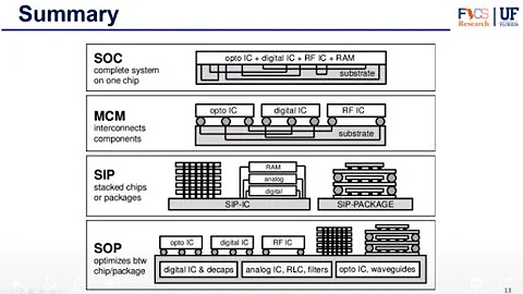
A fabricated wafer contains many semiconductor dies, but a bare die is not normally ready to place on a printed circuit board. Packaging creates the mechanical body and electrical interface needed to handle, test, assemble, cool, and use the device. In a conventional single-die package, the die is attached to a leadframe or substrate, connected by bond wires or flip-chip bumps, protected by a mold compound or lid, and terminated with leads, pads, columns, or solder balls.
Modern packaging can do more than enclose one die. A system-in-package may combine multiple dies and passive components. A 2.5D design may place logic and stacked memory on an interposer. A 3D design may stack active dies directly. For this reason, the package has become part of system architecture rather than a purely protective shell.
The terms chip, die, and package are related but not identical. A die is the piece of processed semiconductor cut from a wafer. A chip is an informal term that may mean a die or a packaged IC depending on context. A package is the assembled structure that surrounds or integrates the die and exposes connections to the next level of the system.
What does an IC package do?
A useful package balances several jobs at the same time:
Electrical connection: routes power, ground, clocks, data, analog, and RF signals between the die and board or between dies.
Mechanical protection: protects fragile silicon and interconnects during handling, assembly, and operation.
Environmental protection: limits exposure to moisture, contamination, and chemicals within the package's rated conditions.
Thermal management: carries heat from the die to exposed pads, leadframes, lids, heat spreaders, heat sinks, or the PCB.
Size and routing transformation: converts microscopic die pads into board-compatible leads, pads, or solder balls.
System integration: can combine chiplets, memory, RF devices, sensors, passives, and other functions in one module.
Testability and manufacturability: provides repeatable interfaces for final test, board assembly, inspection, and rework.
Improving one attribute can make another harder. A very small package may have limited heat-spreading area. A fine-pitch BGA supports many connections but requires more demanding PCB fabrication and inspection. A large multi-die package may deliver high bandwidth but creates difficult power, thermal, warpage, yield, and test problems.
What are the most common IC packaging materials?
There is no single material used for every IC package. Texas Instruments' packaging references describe plastic packages as combinations of a leadframe, die-attach material, bond wire, mold compound, and lead finish. Substrate-based and advanced packages add organic laminates, copper redistribution layers, solder bumps, underfill, interposers, lids, and thermal-interface materials.
| Material or structure | Typical role | Engineering considerations |
|---|---|---|
| Silicon die | Contains the active semiconductor circuits | Die size, thickness, pad layout, edge strength, and power density affect assembly and reliability. |
| Copper-alloy leadframe | Supports the die and forms external leads or exposed pads in many molded packages | Electrical resistance, thermal conduction, plating, moisture sensitivity, and mechanical shape matter. |
| Organic laminate substrate | Routes signals and power under BGA, flip-chip, and multi-die packages | Layer count, trace geometry, via structure, loss, warpage, and coefficient of thermal expansion must be managed. |
| Epoxy mold compound | Encapsulates and protects many plastic packages | Moisture absorption, thermal expansion, adhesion, ionic contamination, and glass-transition behavior affect reliability. |
| Ceramic | Used in selected hermetic, high-temperature, RF, aerospace, and high-reliability packages | Offers stability and hermetic options but generally carries higher material and assembly cost. |
| Gold, copper, or aluminum bond wire | Connects die pads to a leadframe or substrate | Wire material, loop geometry, pad metallurgy, current, and molding stress affect performance and reliability. |
| Copper pillars and solder bumps | Provide flip-chip or die-to-die connections | Pitch, current density, joint fatigue, underfill, coplanarity, and reflow process are important. |
| Silicon or RDL interposer | Creates dense routing between chiplets, logic, and memory in 2.5D systems | Interconnect density, reticle-size scaling, cost, power integrity, and thermal expansion drive selection. |
| Underfill and die attach | Bond components and distribute mechanical stress | Thermal conductivity, modulus, cure profile, voiding, and rework requirements vary by design. |
| Lid, heat spreader, and thermal interface | Move heat from high-power dies toward a cooling solution | Flatness, contact pressure, pump-out, thermal resistance, and material compatibility require validation. |
For mainstream low- and medium-power ICs, a molded plastic package is often the practical baseline. That does not make plastic universally best. Ceramic or metal-lidded constructions may be selected for hermeticity or severe environments, while organic substrates and silicon-based interconnect structures are central to high-I/O and chiplet packages.
What are the main types of IC packaging?
Package names usually describe the external connection style, physical outline, or assembly method. The list below covers common families rather than every JEDEC outline or supplier-specific variation.
| Package family | Connection format | Typical strengths | Main design checks |
|---|---|---|---|
| DIP / PDIP | Two rows of through-hole leads | Easy handling, socketing, prototyping, and visual inspection | Large board area and limited I/O density |
| SOIC / TSSOP / SSOP | Gull-wing leads on two sides | Mature surface-mount assembly and accessible leads | Lead pitch, coplanarity, thermal path, and pin count |
| QFP / TQFP / LQFP | Gull-wing leads on four sides | Visible connections and moderate-to-high pin counts | Fine-pitch soldering, bent leads, package size, and signal escape |
| QFN / DFN | Bottom pads, often with an exposed thermal pad | Small footprint, low lead inductance, and useful thermal path | Stencil design, voiding, wettable flanks, inspection, and exposed-pad layout |
| BGA / FBGA / FCBGA | Area array of solder balls under the package | High I/O density, short connections, and efficient routing for complex devices | PCB layer count, via strategy, warpage, X-ray inspection, and rework |
| LGA | Flat lands under the package | Dense contact array without package-side solder balls | Socket or solder interface, contact pressure, planarity, and land finish |
| WLCSP / DSBGA | Board connections formed at wafer scale close to die size | Very small form factor and short electrical paths | Board-level drop reliability, PCB flex, underfill, and assembly pitch |
| SiP / module | Multiple dies and/or components in one package | Functional integration, reduced board area, and mixed technologies | Known-good-die strategy, test coverage, thermal coupling, repair, and supply coordination |
A package family name alone is not enough to build a footprint. Always use the exact package drawing, land-pattern guidance, moisture-sensitivity information, and reflow requirements for the selected ordering code. Similar names can conceal different dimensions, pitches, exposed pads, ball maps, and height profiles.
How are ICs packaged and tested?
A conventional assembly flow may include wafer thinning, wafer dicing, die attach, wire bonding or flip-chip placement, underfill or molding, plating or ball attach, singulation, marking, inspection, and final test. The exact sequence changes with the package architecture. Wafer-level and panel-level fan-out processes form redistribution and external connections around dies embedded in a reconstructed carrier, while 2.5D and 3D systems require additional interposer, bridge, stacking, bonding, and multi-stage test operations.
Testing occurs at more than one point. Wafer probe can identify known-good dies before expensive assembly. Package-level final test checks the completed device. Complex chiplet systems may also use die sort, intermediate tests, burn-in, system-level test, and repair or redundancy strategies because one bad die can affect the yield of the assembled module.
What is an IC package handler?
A test handler is factory equipment used after packaging. Advantest describes it as equipment that transports devices, controls temperature during semiconductor testing, inserts devices into test interfaces, and sorts them according to test results. The handler does not perform the electrical measurements by itself; it works with a tester and device interface.
Handlers and their change kits must match package dimensions, contact geometry, thermal requirements, force limits, throughput, and orientation. Therefore, the phrase IC package handler refers to test automation equipment, not to a DIP, QFN, BGA, or other package family.
What is the difference between 2D, 2.5D, and 3D packaging?
Industry terminology is not perfectly uniform, but the following model is useful:
2D packaging: one or more dies are mounted on a package substrate or leadframe without a high-density silicon interposer or direct active-die stack.
2.5D packaging: dies sit side by side and communicate through a high-density interposer, redistribution structure, or embedded silicon bridge.
3D packaging: active dies are stacked vertically and connected by TSVs, microbumps, or hybrid bonding.
Fan-out packages do not fit neatly into a simple X-axis-versus-Z-axis classification. They use redistribution layers to extend connections beyond the die footprint and can support single-die or multi-die integration. Similarly, HBM is a stacked-memory technology that becomes part of a larger 2.5D or 3D package; it is not a general-purpose external package family like QFN or BGA.
Fan-out packaging: FOWLP, InFO, and FOPLP
FOWLP: fan-out wafer-level packaging
Fan-out packaging places known-good dies into a reconstructed wafer or carrier, surrounds them with mold material, and forms redistribution layers across both the die and the surrounding fan-out area. The package can route more connections than would fit directly under the original die footprint and may avoid a separate laminate substrate.
FOWLP is used where thin form factor, short connections, and system integration justify the process complexity. Important limits include die-shift control, RDL yield, warpage, package size, thermal design, and board-level reliability.

InFO: TSMC Integrated Fan-Out
InFO is TSMC's fan-out packaging family. TSMC positions InFO for high-density, high-performance mobile, network, and selected HPC integration. The family includes multiple derivatives rather than one universal package structure, so claims about die count, substrate removal, pitch, or target application must be tied to the specific InFO implementation.

FOPLP: fan-out panel-level packaging
FOPLP applies fan-out concepts to rectangular panels. ASE lists panel fan-out platforms using different panel sizes and chip-first or chip-last flows. The potential economic benefit comes from processing more package area per panel and using panel-oriented manufacturing infrastructure, but usable throughput is governed by yield, warpage, placement accuracy, RDL capability, equipment utilization, and package mix. Panel area alone does not prove a proportional cost or throughput improvement.

Bridge and interposer packaging: EMIB and CoWoS
EMIB: embedded multi-die interconnect bridge
Intel's EMIB embeds small silicon bridges in an organic package substrate where high-density die-to-die connections are required. This avoids using a full-size silicon interposer across the entire package while still supporting dense local links between logic, I/O, and memory dies. EMIB is a platform technology with several current derivatives, so pitch, TSV use, capacitor integration, and supported die configurations depend on the selected offering.

CoWoS: chip on wafer on substrate
CoWoS is TSMC's 2.5D advanced packaging family for high-performance systems. CoWoS-S uses a silicon interposer, CoWoS-R uses an RDL interposer, and CoWoS-L combines an RDL-based interposer with embedded local silicon interconnects. These structures can integrate logic chiplets and HBM while providing dense routing, power delivery, and package-level system integration.
CoWoS is not synonymous with every AI accelerator package, and it is not one fixed interposer architecture. Product attribution should be supported by a current vendor or customer announcement rather than inferred from the presence of HBM.

Stacked memory: HBM, HMC, and Wide I/O
HBM: high bandwidth memory
HBM stacks DRAM dies vertically and connects them through a wide interface. TSVs are central to established HBM stack construction, while the assembled stack connects to logic through an interposer or another supported package architecture. HBM offers high aggregate bandwidth close to compute, but it introduces difficult memory-controller, power, thermal, package-yield, and supply-chain requirements.
HBM generation names and performance figures must be taken from the applicable JEDEC standard and the selected memory device. A headline number for one HBM3E or HBM4 implementation cannot be applied to every stack, speed grade, capacity, or accelerator.

HMC: Hybrid Memory Cube
HMC combined stacked DRAM with a logic layer and high-speed serial links. It was an important example of TSV-based 3D memory, but it is now a legacy technology for new commercial designs. Micron states that it moved away from HMC as alternative high-performance memories entered the market and earlier volume programs matured.

Wide I/O and Wide I/O 2
Wide I/O standards were developed for very wide, low-power memory interfaces suited to close integration with mobile logic. They are useful for understanding the evolution of stacked-memory interfaces, but they are not a substitute for checking the memory technology supported by a current application processor or SoC. Treat Wide I/O as a standards and architecture topic rather than a generic package outline.

3D logic and heterogeneous integration
Foveros
Intel's Foveros family stacks chiplets vertically on a base die or interposer structure. Current Intel documentation distinguishes Foveros 2.5D options from Foveros Direct 3D, which uses direct copper-to-copper hybrid bonding for denser die-to-die connections. The thermal, power-delivery, die-test, and mechanical design of a vertical stack must be co-optimized; shorter links alone do not guarantee a successful system.

EMIB 3.5D, formerly described as Co-EMIB
Earlier Intel materials used the name Co-EMIB for designs combining Foveros vertical stacks with EMIB horizontal bridges. Current Intel Foundry material uses EMIB 3.5D for this combined architecture. It is intended for systems that need to connect multiple 3D stacks within one large heterogeneous package.

TSMC-SoIC
TSMC-SoIC is TSMC's front-end 3D chip-stacking technology within the 3DFabric portfolio. It supports stacking similar or dissimilar dies and can use bumpless bonding to create dense vertical connections. SoIC can subsequently be integrated with back-end packaging technologies such as CoWoS, but SoIC and CoWoS describe different levels of the integration flow.
Direct bonding can reduce interconnect pitch and parasitics compared with solder microbumps, but it does not create literally zero resistance, zero latency, or zero signal loss. Surface preparation, alignment, bonding quality, power delivery, heat removal, and test coverage remain critical engineering constraints.

Samsung X-Cube and current 3D packaging
Samsung introduced X-Cube as a 3D integration platform using TSV-based vertical connections. Samsung's original demonstration stacked SRAM over logic, and its current packaging portfolio discusses microbump and hybrid-copper-bonding paths for 3D integration. More recent Samsung material also describes the platform under broader 3D Packaging terminology, so designers should use the current foundry offering name and qualification status for a new project.

How do you choose an IC package architecture?
Start with system requirements rather than a favored package name. The package, die, board, cooling solution, manufacturing line, and test strategy form one design problem.
| Requirement | Questions to answer | Package implications |
|---|---|---|
| I/O and bandwidth | How many signals, at what data rates, with what channel loss and crosstalk limits? | May drive fine-pitch leaded packages, area arrays, flip chip, bridges, interposers, or direct die stacking. |
| Power delivery | What are the current transients, voltage tolerance, return paths, and decoupling needs? | Determines ball map, planes, bump density, substrate stack-up, embedded capacitance, and package size. |
| Thermal design | Where is heat generated, and what junction temperature and cooling method are allowed? | Influences exposed pads, die orientation, lid, heat spreader, thermal interface, stack placement, and package warpage. |
| Mechanical reliability | What are the board bend, drop, vibration, thermal-cycle, humidity, and lifetime requirements? | Changes package size, terminal style, underfill, mold compound, substrate, and board-level qualification. |
| PCB and assembly | Can the board fabricator and assembler support the pitch, via structure, inspection, and rework? | A package that cannot be routed, inspected, or assembled reliably is not a practical choice. |
| Test and yield | Can each die be screened, and can the assembled package be tested, binned, repaired, or traced? | Complex multi-die packages need known-good-die, intermediate test, final test, and failure-analysis plans. |
| Supply and lifecycle | Are the package, substrate, memory, assembly site, and test capacity qualified and available? | Supplier-specific advanced packaging creates additional qualification and capacity dependencies. |
| Cost and volume | What are the die, substrate, mask, tooling, assembly, test, scrap, and yield costs at target volume? | Panel or wafer area is only one input; total good-package cost is the relevant measure. |

Frequently asked questions
What is IC packaging in simple terms?
IC packaging turns a bare semiconductor die into a device that can be protected, tested, cooled, handled, and connected to a circuit board or to other dies.
What are the different types of IC packaging?
Common external package families include DIP, SOIC, TSSOP, QFP, QFN, DFN, BGA, LGA, WLCSP, SiP, and modules. Advanced architectures include fan-out, bridge-based 2.5D, interposer-based 2.5D, TSV-based 3D stacking, and hybrid-bonded 3D stacking.
What is the most common IC packaging material?
Molded plastic packages are widely used in mainstream electronics. They typically combine an epoxy mold compound with a metal leadframe or package substrate, die attach, internal interconnects, and plated external terminals. High-I/O and high-performance packages often rely on organic laminate substrates, while ceramic, silicon, glass, and metal structures serve specialized roles.
What is an IC package handler?
An IC package handler is automated test equipment that moves packaged devices into contact with a semiconductor tester, manages test temperature, and sorts devices by test result. It is not a package type.
What is the difference between traditional and advanced packaging?
Traditional packages typically connect one die to a leadframe or substrate using wire bonds or flip chip. Advanced packaging uses denser redistribution, interposers, bridges, chiplets, TSVs, or direct bonding to integrate multiple dies and achieve system-level bandwidth, size, or functional goals.
What is the difference between FOWLP and CoWoS?
FOWLP embeds dies in a reconstructed carrier and routes connections through fan-out redistribution layers. CoWoS is TSMC's 2.5D family for integrating dies such as logic chiplets and HBM through silicon or RDL-based interposer structures on a package substrate. They address different integration scales and design requirements.
Is HBM an IC package type?
HBM is a stacked DRAM architecture and interface standard, not a general external package family like QFN or BGA. An HBM stack becomes one component within a larger package architecture, often beside logic in a 2.5D system.
Does advanced packaging replace transistor scaling?
No. Advanced packaging complements transistor and process-node improvements by enabling chiplets, heterogeneous integration, wider memory interfaces, shorter die-to-die links, and system-level optimization. It also adds its own cost, yield, power, thermal, test, and reliability constraints.
Conclusion
IC packaging spans everything from molded leadframe devices to multi-die systems built with fan-out RDL, silicon bridges, interposers, TSVs, and hybrid bonding. The package must protect the silicon, connect it electrically, remove heat, survive assembly and operation, and remain testable at acceptable yield and cost.
The most useful first decision is not whether a technology is called 2.5D or 3D. It is whether the complete package architecture meets the product's electrical, thermal, mechanical, manufacturing, test, supply, and lifecycle requirements. Use package-family guides for orientation, then verify the exact supplier platform, package drawing, qualification data, and design rules before committing a design.
References
Texas Instruments: Semiconductor Packaging Assembly Technology
 UTMEL
UTMEL
We are the professional distributor of electronic components, providing a large variety of products to save you a lot of time, effort, and cost with our efficient self-customized service. careful order preparation fast delivery service
1.What is IC packaging and testing?
In electronics manufacturing, integrated circuit packaging is the final stage of semiconductor device fabrication, in which the block of semiconductor material is encapsulated in a supporting case that prevents physical damage and corrosion. The packaging stage is followed by testing of the integrated circuit.
2.Why is IC packaging important?
IC packaging is the ability to provide more and more I/O interconnections to a die (bare chip) that is increasingly shrinking in size is an ever-present problem. This will imposes challenges for new 3D integration that requires innovative packaging technologies.
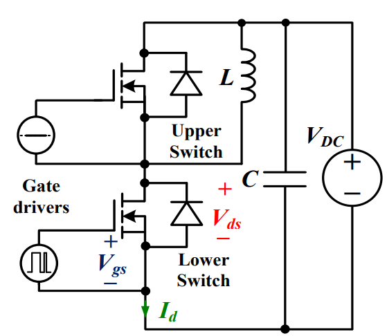 Discovering New and Advanced Methodology for Determining the Dynamic Characterization of Wide Bandgap DevicesSaumitra Jagdale15 March 20242871
For a long era, silicon has stood out as the primary material for fabricating electronic devices due to its affordability, moderate efficiency, and performance capabilities. Despite its widespread use, silicon faces several limitations that render it unsuitable for applications involving high power and elevated temperatures. As technological advancements continue and the industry demands enhanced efficiency from devices, these limitations become increasingly vivid. In the quest for electronic devices that are more potent, efficient, and compact, wide bandgap materials are emerging as a dominant player. Their superiority over silicon in crucial aspects such as efficiency, higher junction temperatures, power density, thinner drift regions, and faster switching speeds positions them as the preferred materials for the future of power electronics.
Read More Applications of FPGAs in Artificial Intelligence: A Comprehensive GuideUTMEL29 August 20255555
This comprehensive guide explores FPGAs as powerful AI accelerators that offer distinct advantages over traditional GPUs and CPUs. FPGAs provide reconfigurable hardware that can be customized for specific AI workloads, delivering superior energy efficiency, ultra-low latency, and deterministic performance—particularly valuable for edge AI applications. While GPUs excel at parallel processing for training, FPGAs shine in inference tasks through their adaptability and power optimization. The document covers practical implementation challenges, including development complexity and resource constraints, while highlighting solutions like High-Level Synthesis tools and vendor-specific AI development suites from Intel and AMD/Xilinx. Real-world applications span telecommunications, healthcare, autonomous vehicles, and financial services, demonstrating FPGAs' versatility in mission-critical systems requiring real-time processing and minimal power consumption.
Read More The 2026 Engineer’s Guide: Choosing the Right MCU for Your Next IoT & New Energy ProjectUTMEL30 April 20261792
A comprehensive comparison of 2026's leading MCUs from ST, NXP, and Microchip across power efficiency, processing performance, connectivity, and ecosystems to help engineers select the optimal chip for next-gen IoT and new energy projects.
Read More AI Server Components: Engineering Next-Gen Data Center Hardware for 100kW RacksUTMEL15 May 2026983
The transition from traditional enterprise IT to AI-driven workloads has rendered legacy data center hardware obsolete, forcing infrastructure planners to re-engineer server components for extreme thermal environments.
Read More The Practical Engineer’s Guide to the NE555N Timer: Pinout, Setup, and TroubleshootingUTMEL29 May 2026770
This comprehensive guide explores the NE555N timer, detailing its 8-pin layout, internal architecture, and key datasheet specifications. It compares the bipolar IC to CMOS variants and details setup configurations for astable, monostable, and bistable modes. Additionally, the guide offers practical troubleshooting advice to prevent common breadboard failures, such as floating reset pins and electrical noise issues.
Read More
Subscribe to Utmel !
![ATAES132A-MAHEQ-T]() ATAES132A-MAHEQ-T
ATAES132A-MAHEQ-TMicrochip Technology
![ATECC508A-SSHCZ-B]() ATECC508A-SSHCZ-B
ATECC508A-SSHCZ-BMicrochip Technology
![HCS360-I/P]() HCS360-I/P
HCS360-I/PMicrochip Technology
![HCS361-I/SN]() HCS361-I/SN
HCS361-I/SNMicrochip Technology
![FOD410SD]() FOD410SD
FOD410SDON Semiconductor
![FOD4108SD]() FOD4108SD
FOD4108SDON Semiconductor
![HCS515-I/P]() HCS515-I/P
HCS515-I/PMicrochip Technology
![AL1788W6-7]() AL1788W6-7
AL1788W6-7Diodes Incorporated
![MOC3083SM]() MOC3083SM
MOC3083SMON Semiconductor
![FOD4118]() FOD4118
FOD4118ON Semiconductor


