Product
 Brand
Brand Articles
 Tools
Tools
Top 5 Microcontrollers Defining IoT, Edge AI, and Power Efficiency in 2026: Sourcing and Selection Guide
Executive Summary
Selecting a microcontroller (MCU) in 2026 requires balancing edge AI inference capabilities, contiguous SRAM limits, energy duty cycling, and mature-node procurement lead times. As machine learning workloads shift from centralized cloud infrastructure to tiny localized endpoints, traditional selection metrics—such as clock speed (MHz) or unit price alone—fail to capture total system cost and battery longevity.
The microcontrollers defining 2026 embedded architectures address distinct engineering trade-offs:
Espressif ESP32-S3: The low-cost Wi-Fi/Bluetooth standard featuring 128-bit vector SIMD instructions for localized TinyML workloads.
STMicroelectronics STM32U5: The industrial benchmark for ultra-low power consumption, autonomous peripheral execution, and PSA Certified Level 3 security.
Texas Instruments MSPM0G5187: A real-time control MCU pairing mixed-signal precision with an integrated TinyEngine INT8 NPU hardware accelerator.
WCH CH32V003: An ultra-budget 32-bit RISC-V core engineered to replace legacy 8-bit controllers and reduce Bill-of-Materials (BOM) costs.
Nordic Semiconductor nRF54 Series: A multi-core wireless System-on-Chip (SoC) built on a 22nm process node for Bluetooth 5.4, Mesh, and LE Audio environments.
The 2026 MCU Selection Architecture: Balancing Compute, SRAM, Power, and Ecosystem
The Memory Bottleneck in Edge AI
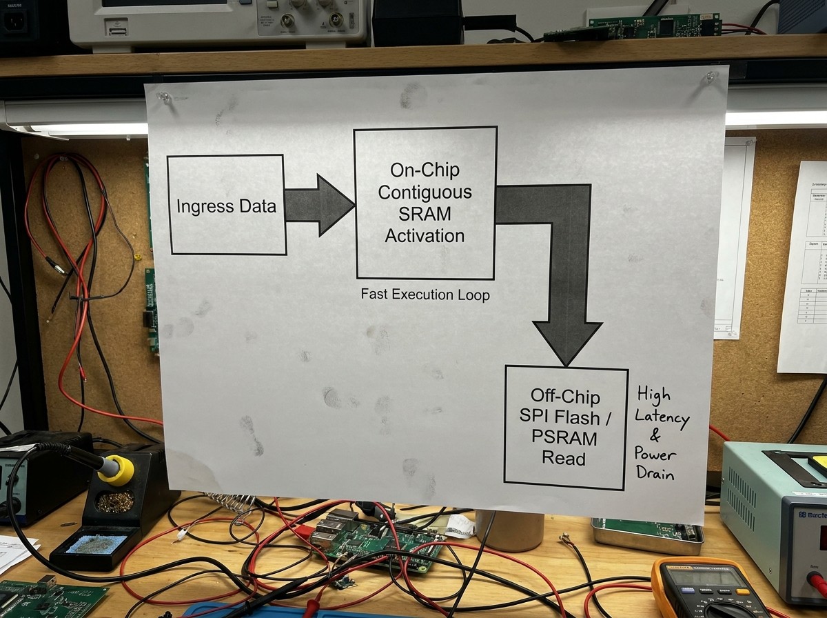
In TinyML and edge neural network execution, contiguous SRAM capacity is the primary performance bottleneck[4], often overriding raw CPU clock speed. Machine learning model tensor activations must reside in fast internal RAM during inference.
If intermediate activations exceed available SRAM, the MCU is forced to read and write weights to external SPI Flash, introducing severe bus latencies and accelerating battery drain. Evaluating an Edge AI MCU requires verifying that uncompressed model activations fit cleanly within internal SRAM boundaries.
Energy Efficiency vs. Peak Compute
System energy consumption is governed by active current, deep-sleep leakage, and dynamic duty cycling:
Total Energy = (Iactive × tactive) + (Isleep × tsleep)
Executing an AI model rapidly at high active current and immediately dropping into a microampere or nanoampere sleep mode (duty cycling) often consumes less net energy than running a low-frequency core continuously.
The Ecosystem "HR Hack"
Selecting an MCU family with widespread industry adoption serves as an engineering organization accelerator. Standard architectures like the Arm Cortex-M ecosystem or popular ESP32 variants provide mature software libraries, CMSIS-NN support, and broad developer familiarity. Choosing established silicon reduces team onboarding friction, speeds up firmware validation, and lowers Non-Recurring Engineering (NRE) costs.
The Certification Bypass Strategy
Designing discrete RF layouts with bare silicon SoCs requires antenna tuning, impedance matching, and expensive regulatory compliance testing (FCC, CE, Anatel). For low-to-medium production volumes (<100,000 units), using pre-certified wireless modules (such as the ESP32-S3-WROOM series) bypasses compliance delays, potentially saving tens of thousands of dollars in testing fees and reducing time-to-market by several months.
Decision Matrix: System Requirements to MCU Selection
| Application Need | Primary Constraint | Recommended MCU Family | Key Architectural Reason |
|---|---|---|---|
| Wi-Fi/BLE Smart Devices | Budget & Connectivity | Espressif ESP32-S3 | Dual LX7 cores with vector math; cheap module ecosystem. |
| Battery-Powered Wearables | Microampere Leakage | STMicroelectronics STM32U5 | LPBAM peripheral running in Stop modes down to 1.7 µA. |
| Industrial Analog Control | Real-Time Latency | TI MSPM0G5187 | Integrated INT8 NPU acceleration + high-speed ADCs. |
| Housekeeping & Simple Control | BOM Cost (< $0.20) | WCH CH32V003 | 32-bit RISC-V core replacing legacy 8-bit ICs. |
| Advanced BLE 5.4 / Mesh | RF Efficiency & Audio | Nordic nRF54 Series | Multi-core 22nm architecture with low nJ/bit radio metrics. |
Why Generic AI Summaries and Traditional MCU Rankings Fall Short in 2026
Automated search summaries and generic online rankings often rely on outdated datasheet specs, leading engineering and procurement teams into design traps:
The "TOPS Trap": Marketing claims highlighting high theoretical GFLOPS or TOPS metrics often mask severe thermal dissipation and memory bus bottlenecks. An NPU core cannot achieve its rated compute output if the system bus cannot feed input tensors fast enough.
The Unit Price Illusion: Evaluating a component based strictly on unit cost risks overlooking total product development costs. A sub-dollar chip lacking driver documentation or RTOS integration can incur tens of thousands of dollars in custom firmware development.
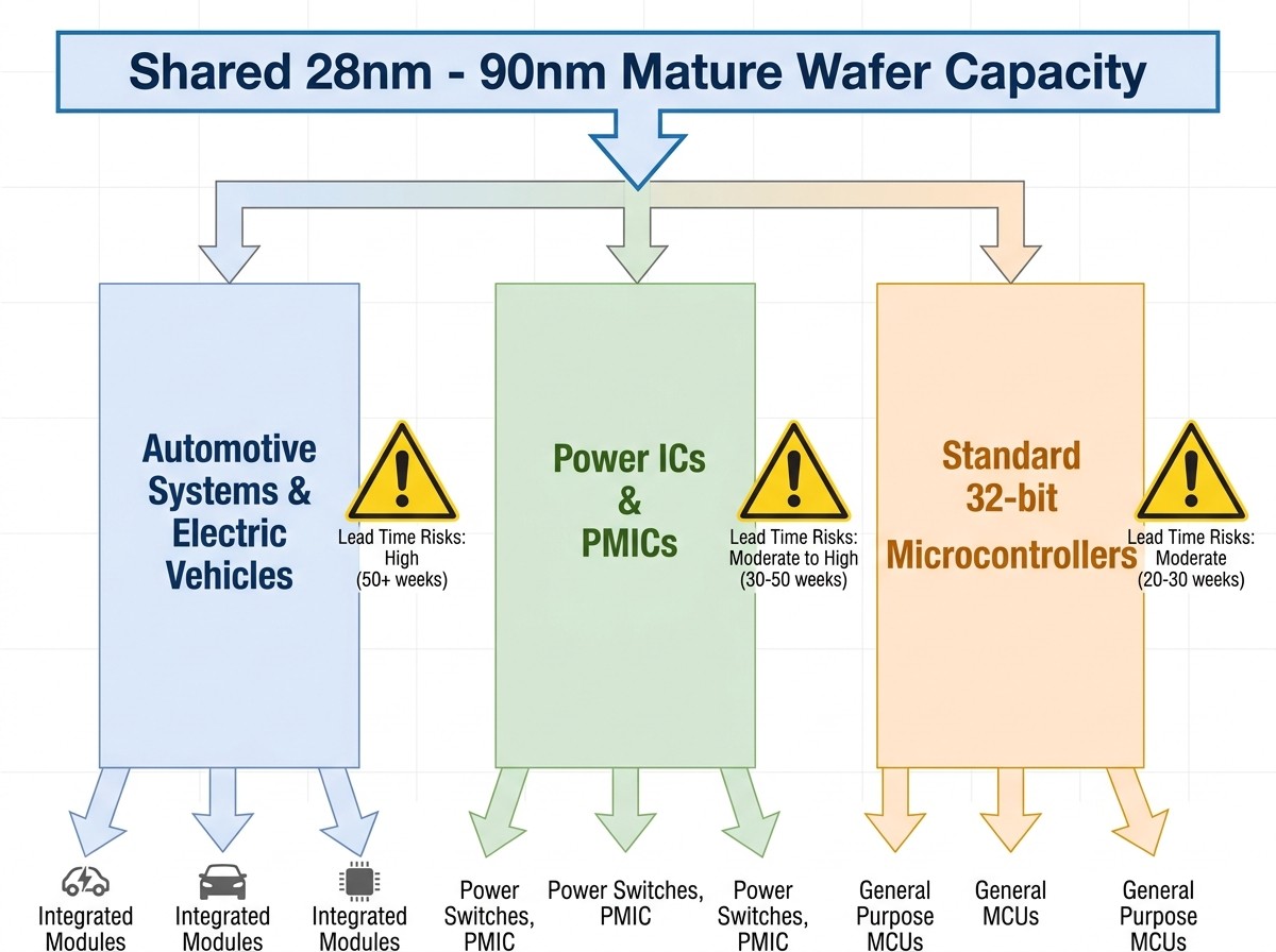
Mature-Node Capacity Bottlenecks: Standard 28nm, 40nm, and 90nm mature fab nodes face manufacturing competition from automotive power electronics and AI data-center support ICs. Even if spot inventory appears available, global lead times can shift rapidly.
2026 Technical Spec & Trade-off Matrix: Top 5 MCUs Compared
| MCU Family | Core Architecture & Speed | Internal SRAM / Flash Limits | Wireless Connectivity | Hardware Acceleration | Active / Sleep Profile | Primary Target Application |
|---|---|---|---|---|---|---|
| Espressif ESP32-S3 | Dual-Core Xtensa LX7 @ 240 MHz | 512 KB SRAM / 384 KB ROM (Ext. Flash/PSRAM) | Wi-Fi 4 (802.11b/g/n) & BLE 5.0 | 128-bit Vector SIMD Extensions | ~240 mA (Wi-Fi TX peak) / ~8 µA (Deep Sleep) | Low-Cost AIoT, Smart Home Voice/Vision |
| STMicroelectronics STM32U5 | Single Arm Cortex-M33 @ 160 MHz | Up to 3 MB SRAM / Up to 4 MB Flash | Host MCU (External RF module optional) | AES/PKA Crypto, TrustZone | 19 µA/MHz (Active) / 1.7 µA (Stop 3 w/ 16KB RAM) | Secure Medical, Industrial Battery Sensors |
| TI MSPM0G5187 | Single Arm Cortex-M0+ @ 80 MHz | 32 KB SRAM / 128 KB Flash | Host MCU (Wired CAN FD, LIN, SPI) | Integrated TinyEngine INT8 Hardware NPU | ~80 µA/MHz (Active) / ~1.5 µA (Standby) | Motor Control, Inverters, Smart Telemetry |
| WCH CH32V003 | 32-bit QingKe RISC-V2A @ 48 MHz | 2 KB SRAM / 16 KB CodeFlash | None (Wired GPIO, I2C, SPI, USART) | Hardware Multiply/Divide, Single-Wire Debug | ~5 mA (Active @ 48MHz) / ~10 µA (Standby) | Housekeeping, Power Sequencing, Toy/BOM Cut |
| Nordic nRF54 Series | Multi-Core Cortex-M33 (up to 320 MHz) | Up to 1 MB SRAM / Up to 2 MB NVM | BLE 5.4, Thread, Matter, LE Audio | Dedicated Crypto & RISC-V Radio Cores | Ultra-low nJ/bit radio TX/RX, sub-µA System OFF | Medical Wearables, Premium Audio, Asset Tracking |
Detailed Breakdown: Top 5 Microcontrollers Dominating 2026 Designs
Top 5 Microcontrollers in 2026 - Best Performance for the Price
1. Espressif ESP32-S3 Series: The Benchmark for Low-Cost AIoT and Localized TinyML
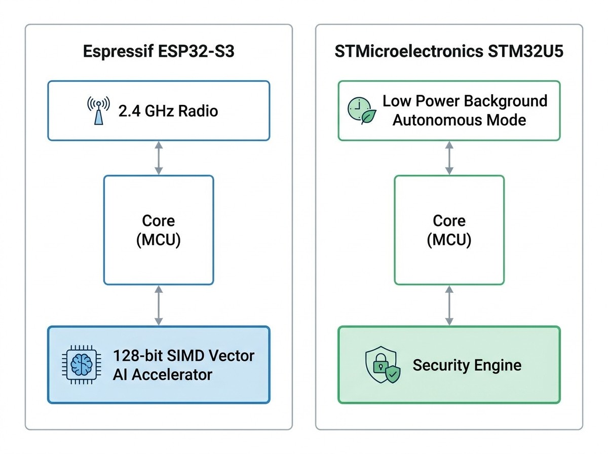
The ESP32-S3 combines dual-core processing[1], native wireless connectivity, and vector math extensions for budget-conscious connected devices.
Key Technical Capabilities
Core & Compute: Dual-core 32-bit Xtensa LX7 operating up to 240 MHz, yielding a CoreMark score of 1329.92 (5.54 CoreMark/MHz)[1].
Vector Extensions: Incorporates 128-bit vector instructions accessible via ESP-DSP and ESP-NN libraries, accelerating matrix multiplication and FIR/IIR filtering for local keyword spotting and anomaly detection.
Connectivity: Integrated 2.4 GHz Wi-Fi 4 (802.11 b/g/n) and Bluetooth 5.0 (LE) with long-range support.
Strengths & Advantages
Ecosystem Support: Supported by ESP-IDF, FreeRTOS, Arduino, and major machine learning deployment tools like Edge Impulse.
Pre-Certified Modules: Available in ESP32-S3-WROOM and ESP32-S3-MINI modules, reducing regulatory compliance delays.
Hidden Trade-offs & Limitations
Power Draw: Deep-sleep current draw (~8 µA) and active Wi-Fi transmit current spikes (~240 mA peak) make it less suited for non-rechargeable coin-cell battery applications.
Best For: Smart home voice control nodes, low-cost vision sensors, and connected IoT gateways.
Who Should NOT Choose It: Ultra-low-power industrial telemetry endpoints designed to operate on a single CR2032 battery for 10 years.
---
2. STMicroelectronics STM32U5 Series: The Gold Standard for Ultra-Low Power and Security
The STM32U5 provides extreme energy efficiency and high-grade hardware security for demanding industrial and medical designs.
Key Technical Capabilities
Power Management: Arm Cortex-M33 running at 160 MHz, consuming 19 µA/MHz[2] in active mode.
Autonomous Execution: Features Low Power Background Autonomous Mode (LPBAM), allowing Direct Memory Access (DMA) and peripherals to process sensor data in Stop modes down to 1.7 µA without waking the main CPU core.
Hardware Security: Holds PSA Certified Level 3 and SESIP Level 3 security qualifications[2], featuring TrustZone isolation, active tamper detection, and side-channel attack resistant hardware cryptography.
For an in-depth breakdown of power states and memory protection structures in this family, see our detailed analysis of the STM32U5 architecture.
Strengths & Advantages
Ecosystem Familiarity: Uses standard STM32Cube tools, simplifying development for engineering teams with prior ARM architecture experience.
Large Memory Footprint: Offers up to 3 MB of contiguous internal SRAM and 4 MB of dual-bank Flash.
Hidden Trade-offs & Limitations
Unit Cost & Complexity: Higher unit price compared to basic 32-bit microcontrollers, requiring complex power-mode switching configurations in firmware.
Best For: Wearable medical monitors, smart utility meters, and secure industrial IoT endpoints.
Who Should NOT Choose It: High-volume consumer products requiring single-die integrated Wi-Fi connectivity on a tight BOM budget.
---
3. Texas Instruments MSPM0G5187: Real-Time Control with Hardware Edge AI Acceleration
The MSPM0G5187 brings hardware-accelerated neural network inference to cost-sensitive real-time control applications.
Key Technical Capabilities
Architecture: Arm Cortex-M0+ running at 80 MHz paired with 128 KB Flash and 32 KB SRAM.
TinyEngine NPU: Features an integrated hardware NPU engine designed for quantized INT8 neural networks[3], executing inference layers in single clock cycles without software floating-point emulation.
Analog Integration: Integrates high-speed 12-bit ADCs, operational amplifiers, and high-resolution PWM timers for high-frequency control loops.
Strengths & Advantages
Low-Latency Inference: Hardware-level NPU execution delivers low latency for fault detection (e.g., arc fault or motor vibration analysis) alongside primary control loops.
Mixed-Signal Efficiency: Reduces external component count by internalizing precision analog front-ends.
Hidden Trade-offs & Limitations
Memory Limits: 32 KB SRAM limits memory space, restricting model size to small, targeted classification networks.
Best For: Smart motor drives, solar micro-inverters, power distribution units, and automated circuit breakers.
Who Should NOT Choose It: High-resolution image processing applications or nodes requiring native on-chip wireless transceivers.
---
4. WCH CH32V003: The Open-Source RISC-V Powerhouse Cutting BOM Costs
The CH32V003 targets basic control tasks, offering a 32-bit RISC-V core at a price point competitive with legacy 8-bit microcontrollers.
Key Technical Capabilities
Core Architecture: 32-bit QingKe RISC-V2A core (RV32EC instruction set) operating up to 48 MHz.
Memory & I/O: 2 KB SRAM, 16 KB CodeFlash, 1-wire debug interface, 10-bit ADC, and standard serial communication interfaces (I2C, SPI, USART).
Voltage Range: Operates across 2.7V to 5.5V, making it directly compatible with 5V industrial logic without external level translators.
Strengths & Advantages
BOM Cost Reduction: Reported near ~$0.10 in volume production, providing 32-bit processing at 8-bit pricing levels, though this figure should be verified with current distributor quotes.
Compact Packaging: Available in small SOP8, TSSOP20, and QFN20 footprint options.
Hidden Trade-offs & Limitations
Software Ecosystem Maturity: Lacks standard ARM CMSIS libraries; firmware teams must rely on WCH drivers or community-maintained bare-metal toolchains.
Best For: Power sequencing, LED control, simple sensor interface bridging, consumer electronics, and high-volume BOM cost reduction.
Who Should NOT Choose It: Complex edge AI workloads, heavy DSP math, or multi-protocol wireless networking projects.
---
5. Nordic Semiconductor nRF54 Series: Next-Gen Ultra-Low Power for BLE 5.4 & Wearables
The nRF54 Series establishes an energy-efficiency benchmark for multi-protocol wireless endpoints and body-worn sensors.
Key Technical Capabilities
Advanced Process Node: Fabricated on a 22nm low-leakage process node[4], lowering active radio current consumption and static leakage.
Multi-Core Architecture: Integrates application processing, security, and a dedicated RISC-V radio coprocessor, with top-tier variants (nRF54H20) scaling up to 320 MHz.
RF Capabilities: Native support for Bluetooth 5.4, Bluetooth Mesh, Thread, Matter, and LE Audio, with -98 dBm RX sensitivity and up to +8 dBm TX power.
Strengths & Advantages
Radio Energy Efficiency: Low nJ/bit energy metrics extend operating life on compact lithium-ion or coin-cell batteries.
High Processing Density: Multi-core execution isolates real-time RF tasks from application software.
Hidden Trade-offs & Limitations
Unit Price: Commands a premium unit cost, making it excess expenditure for non-wireless applications.
Best For: Continuous glucose monitors, medical wearables, high-density asset tracking tags, and wireless audio equipment.
Who Should NOT Choose It: Stationary wired industrial controllers without wireless requirements.
---
2026 Supply Chain Reality: Lead Times, Allocation Risks, and Pricing Trends
Mature Node Bottlenecks (28nm – 90nm)
Microcontroller manufacturing relies heavily on mature wafer nodes (28nm, 40nm, 55nm, and 90nm). In 2026, capacity allocation constraints persist on these lines due to competing demand from automotive electrification systems and power management sub-systems.
While lead times for standard off-the-shelf consumer SKUs have stabilized to typical window periods, specialized automotive-grade (AEC-Q100) and industrial high-reliability part numbers may experience extended delivery lead times, though confirmed 2026 week-range data is not yet publicly available from primary foundry or distributor sources.
Upstream Pricing Pressures
Substrate costs, advanced packaging utilization, and raw material pricing adjustments continue to exert upward pressure on finalized component BOMs.
Procurement specialists should monitor broader semiconductor trends to anticipate component pricing shifts. For detailed analysis, see our 2026 power management IC supply risks and sourcing strategies and our 2026 semiconductor component price trends analysis.
---
Strategic Sourcing: Navigating Shortages and Authentication with UTMEL
To maintain factory line continuity during supply allocations, procurement and hardware design teams must combine early schematic planning with reliable component sourcing.
1. Pin-Compatible Second-Sourcing
Design dual-footprint printed circuit boards (PCBAs) during layout to support drop-in or near-drop-in MCU alternatives. Laying out traces to accommodate pin-compatible variants across ARM or RISC-V platforms prevents total board redesigns if a primary SKU experiences sudden lead-time allocation.
2. Sourcing via Direct Inventory Platforms
During supply constraints, authorized distribution channels may face extended backorders. Partnering with direct stocking distributors like UTMEL Electronics provides access to available inventory, direct-sourcing options, and component selection support across major silicon manufacturers.
Explore UTMEL's extensive microcontroller catalog to verify stock availability and component parameters.
3. Anti-Counterfeiting and Part Authentication
Extended lead times increase the circulation of non-factory-new, remarked, or counterfeit components in the spot market. Sourcing strategy requires rigorous quality testing before board assembly:
Visual & Marking Inspection: Confirming top-mark laser engraving consistency, pin plating integrity, and original manufacturer packaging indicators.
X-Ray Inspection: Verifying wire-bond layouts, internal leadframe geometry, and die structure against known factory baselines.
Decapsulation & Die Verification: Exposing internal silicon to confirm original semiconductor manufacturer logos and mask revisions.
---
Datasheet & Engineering Selection Verification Checklist
Before locking schematic symbols and generating a final production Bill of Materials, complete these six verification steps:
[ ] 1. Contiguous SRAM Verification: Does the uncompressed neural network activation layer fit within internal SRAM without requiring external SPI Flash paging?
[ ] 2. Sleep Current Battery Life Audit: Is the calculated sleep-mode leakage current low enough to hit targeted battery lifespan goals?
[ ] 3. RF Compliance Strategy: Does the project budget allocate funds for bare SoC antenna tuning and regulatory certification (FCC/CE), or is a pre-certified module required?
[ ] 4. Software Ecosystem Assessment: Are open-source drivers, CMSIS-NN libraries, or vendor HALs mature enough to support target development timelines?
[ ] 5. Supply Chain Availability: Is the selected SKU available through direct stocking inventory providers such as UTMEL, and have drop-in alternative SKUs been identified?
[ ] 6. Longevity Commitment: Has the silicon manufacturer pledged a 10-to-15-year availability program for the chosen part family?
---
Frequently Asked Questions (FAQ)
How do I choose between an Arm Cortex-M MCU and a RISC-V MCU for Edge AI?
Arm Cortex-M microcontrollers offer a mature ecosystem supported by standard software tooling, vendor Hardware Abstraction Layers (HALs), and optimized CMSIS-NN libraries. RISC-V MCUs eliminate architecture licensing fees, offering lower unit costs and flexible custom instruction sets. However, RISC-V platforms often require firmware engineering teams to maintain custom bare-metal drivers and toolchains.
Why is contiguous SRAM capacity more critical than clock speed (MHz) for TinyML?
Neural network model layers process intermediate data arrays (tensors) that must reside in fast memory during inference. If an MCU lacks sufficient contiguous SRAM, it must frequently stream data from slower external SPI Flash. This bus bottleneck degrades overall inference speed and increases dynamic power consumption regardless of how fast the CPU core operates.
When should an engineering team choose a pre-certified RF module over a bare MCU SoC?
Pre-certified RF modules (such as the ESP32-S3-WROOM series) are recommended for low-to-medium production volumes (<100,000 units). Modules bypass expensive FCC/CE regulatory testing and RF antenna design costs, shortening time-to-market. For high-volume mass production (>500,000 units), transitioning to a bare SoC layout reduces individual unit BOM costs enough to offset upfront RF engineering and certification expenses.
How can procurement teams safeguard MCU supply chains against mature-node allocation spikes?
Procurement teams should establish rolling 6-to-12-month demand forecasts, design pin-compatible secondary MCU footprints into PCB layouts, and utilize direct-sourcing platforms such as UTMEL Electronics to secure stock during allocation periods.
Sources and references used for this guide
ESP32-S3 Series - Espressif Documentation
Source type: official company documentation
Used for: Technical specifications for the ESP32-S3 microcontroller, including Wi-Fi, BLE, and vector instructions.
Caution: Official datasheet; use for technical capabilities, not market share claims.STM32U5 series of Ultra-low-power MCUs
Source type: official company documentation
Used for: Technical specifications for the STM32U5 series, focusing on ultra-low power and TrustZone security.
Caution: Official product page; use for features, not comparative rankings.MSPM0G5187 Evaluation Module User's Guide
Source type: official company documentation
Used for: Confirmation of the MSPM0G5187 product family and basic evaluation parameters.
Caution: Evaluation guide; does not contain full NPU performance metrics.Edge AI On MCUs: The Practical Buyer's Guide
Source type: industry institution
Used for: Background context on selecting MCUs for Edge AI, including SRAM and NPU considerations.
Caution: Industry guide; use for decision framework concepts.
 UTMEL
UTMEL
We are the professional distributor of electronic components, providing a large variety of products to save you a lot of time, effort, and cost with our efficient self-customized service. careful order preparation fast delivery service
 Getting Started with Arduino: What is Arduino and How to Use Arduino BoardsUTMEL28 September 20237216
Arduino is an open-source electronics platform that includes software and programmable circuit boards, allowing beginners to build electronic projects by writing simple code. The article provides an overview of Arduino, including different board types, basic components, how to use the boards, and project ideas like an automated plant watering system.
Read More IoT Chips Lead Time 2026: Navigating MCU, PMIC, and Sensor ShortagesUTMEL15 July 2026837
Navigating component supply and allocation challenges in the 2026 IoT market. This procurement trend brief provides electronics engineers and component sourcing teams with a data-driven analysis of the IoT chips lead time 2026 landscape, detailing supply bottlenecks and alternative design strategies.
Read More MCU with Built-in NPU: How to Pick an Edge AI Microcontroller in 2026UTMEL30 July 20261309
Evaluating Edge AI microcontrollers requires looking beyond vendor-quoted TOPS metrics. This guide explains how to segment candidate parts into sensor, control, or vision tiers, calculate binding SRAM constraints, verify NPU operator support to avoid CPU fallbacks, and navigate production lifecycle risks. Follow a practical five-step engineering sequence to benchmark real models on physical evaluation boards.
Read More Top 5 Microcontrollers Defining IoT, Edge AI, and Power Efficiency in 2026: Sourcing and Selection GuideUTMEL15 August 2026696
This guide reviews the top five microcontrollers defining 2026 embedded designs—ESP32-S3, STM32U5, MSPM0G5187, CH32V003, and nRF54. It evaluates how contiguous SRAM limits, power duty cycling, and hardware acceleration impact edge AI and IoT performance. It also details strategic procurement methods for navigating mature-node supply chain risks, dual-footprint layouts, and component authentication.
Read More Arduino vs. Raspberry Pi: A Detailed ComparisonUTMEL24 April 20255806
Hello everyone, welcome to the new post today.This guide is going to talk in detail about Arduino vs. Raspberry Pi to clarify their differences and help you pick the right board based on your needs.
Read More
Subscribe to Utmel !
![MT9HVF12872PKZ-80EH1]() MT9HVF12872PKZ-80EH1
MT9HVF12872PKZ-80EH1Micron Technology Inc.
![MT16HTF51264HZ-800C1]() MT16HTF51264HZ-800C1
MT16HTF51264HZ-800C1Micron Technology Inc.
![MT8HTF12864HZ-800M1]() MT8HTF12864HZ-800M1
MT8HTF12864HZ-800M1Micron Technology Inc.
![KIT-14180]() KIT-14180
KIT-14180SparkFun Electronics
![APCFA004GGDAN-W6FT]() APCFA004GGDAN-W6FT
APCFA004GGDAN-W6FTApacer Memory America
![AJ6.112GGA.00110]() AJ6.112GGA.00110
AJ6.112GGA.00110Apacer Memory America
![AJ6.112FHA.00110]() AJ6.112FHA.00110
AJ6.112FHA.00110Apacer Memory America
![AA2.259HZA.001E9]() AA2.259HZA.001E9
AA2.259HZA.001E9Apacer Memory America
![D12.31285S.001]() D12.31285S.001
D12.31285S.001Apacer Memory America
![AJ6.112JHA.00110]() AJ6.112JHA.00110
AJ6.112JHA.00110Apacer Memory America