

 Product
 Brand
Brand Articles
 Tools
Tools
Why Hybrid Bonding is Replacing Solder Bumps in Advanced 3D Packaging
Executive Summary & Decision Framework
As semiconductor process scaling under traditional Dennard scaling slows, the industry has shifted toward heterogeneous integration—stacking active logic, cache, and high-bandwidth memory dies vertically to preserve performance gains. For over two decades, microbumps (copper pillars capped with tin-silver solder) served as the primary interconnect for 2.5D and 3D System-in-Package (SiP) architectures. However, at an interconnect pitch below 10 micrometers (μm), traditional solder bumps hit physical, electrical, and thermal limits[1].
Direct copper-to-copper (Cu-Cu) dielectric hybrid bonding eliminates solder entirely. By embedding copper contact pads flush within a polished dielectric surface (SiO2 or SiCN), hybrid bonding enables direct atomic contact between dies. This "bumpless" packaging technique shrinks interconnect pitches to 0.8–9 μm in commercial production—with research roadmaps scaling down to sub-0.5 μm[5]—boosting vertical interconnect density to over 250,000–1,000,000 pads/mm2.
For packaging architects, system designers, and procurement managers, selecting between traditional microbumps, thermo-compression bonding (TCB), and hybrid bonding requires balancing density requirements, thermal budgets, yield constraints, and overall packaging costs.
3D Packaging Technology Selection Framework
| Selection Metric | Mass Reflow / Microbumps | Thermo-Compression Bonding (TCB) | Chip-to-Wafer (C2W) Hybrid Bonding | Wafer-to-Wafer (W2W) Hybrid Bonding |
|---|---|---|---|---|
| Target Interconnect Pitch | ≥ 35 μm | 10 μm – 35 μm | 1 μm – 10 μm | <0.5 μm – 9 μm |
| Interconnect Density | 400 – 800 pads/mm2 | 800 – 1,600 pads/mm2 | 10,000 – 100,000 pads/mm2 | >250,000 – 1,000,000 pads/mm2 |
| Interconnect Material | Cu Pillar + Sn/Ag Solder | Cu Pillar + Micro-Solder Cap | Direct Cu-Cu + SiO2/SiCN | Direct Cu-Cu + SiO2/SiCN |
| Die Matching Requirement | Mismatched die sizes allowed | Mismatched die sizes allowed | Mismatched die sizes allowed (KGD testing) | Strict 1:1 die size and footprint match |
| Cleanroom Standard | ISO 5 / Class 100 | ISO 4 / Class 10 | ISO 3 / Class 1 | ISO 3 / Class 1 |
| Primary Failure Modes | Solder bridging, IMC voiding | Solder squeeze-out, non-wetting | CMP dishing void, particle defects | Wafer warpage, overlay misalignment |
| Best-For Applications | Standard 2.5D interposers, legacy GPUs | HBM3 / HBM3e base stacks, consumer SiPs | Heterogeneous AI chiplets, mixed-node 3D ICs | CIS, 3D V-Cache, 16-Hi HBM4 memory stacks |
Technical Comparison: Microbumps vs. Direct Hybrid Bonding
To understand why advanced 3D packaging is shifting to bumpless integration, engineers must evaluate how microbumps and hybrid bonding differ across fundamental physical and operational parameters.
Comparative Specification Matrix
| Engineering Parameter | Solder Microbump Packaging | Direct Cu-Cu Hybrid Bonding |
|---|---|---|
| Minimum Pitch Scale | 10 μm – 40 μm (Volume std: 25 μm) | 0.8 μm – 9 μm (Commercial); <0.5 μm (Roadmap) |
| Vertical Gap (Z-Height) | 10 μm – 30 μm solder standoff | Imperceptible / Near-zero gap (~0 μm) |
| Underfill Requirement | Required (Capillary Underfill or MR-MUF) | None (Eliminated via direct dielectric bond) |
| Parasitic Capacitance | High (~5 – 15 fF per bump) | Sub-femtofarad (<0.2 fF per pad) |
| Interconnect Resistance | Higher (mΩ range per joint) | Near-zero (μΩ range across metal interface) |
| Thermal Standoff Impedance | Elevated by organic underfill layer | Low (Direct inorganic oxide-to-oxide path) |
| Bonding Mechanism | Liquid-phase metallurgical reflow | Room-temp dielectric fusion + thermal Cu diffusion |
| Cleanroom Requirements | Standard packaging facility (Class 100/1000) | Ultra-clean fab environment (ISO 3 / Class 1) |
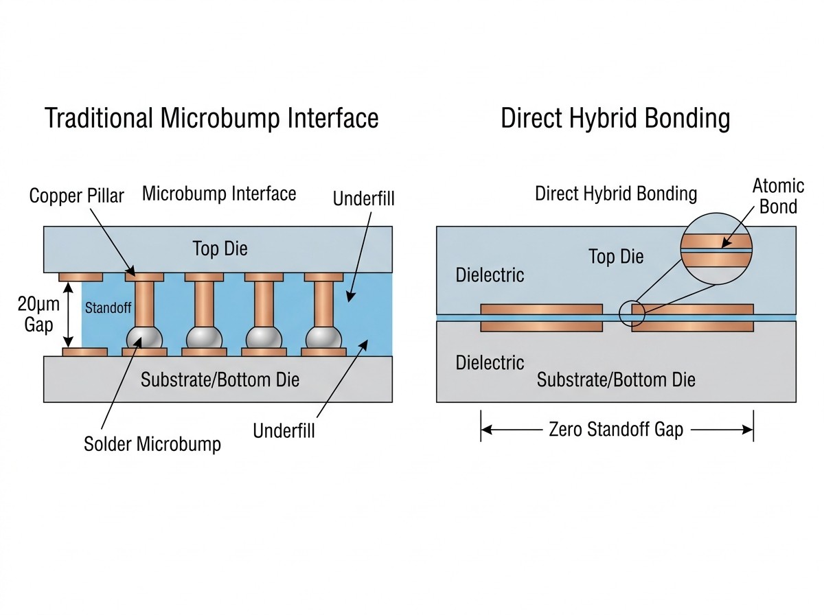
Traditional Microbump Interface                Direct Hybrid Bonding Interface
+-------------------------------+              +-------------------------------+
|          Top Die              |              |          Top Die              |
|  +-----+           +-----+    |              |  |  Cu  |           |  Cu  |    |
|  | Cu  |           | Cu  |    |              |  | Pad  | Dielectric| Pad  |    |
+--+-----+-----------+-----+----+              +--+------+-----------+------+----+
|  | Sn | Underfill | Sn |     |  <-- 20µm Gap  =================================  <-- Atomic Bond
+--+-----+-----------+-----+----+              +--+------+-----------+------+----+
|  | Cu  |           | Cu  |    |              |  | Cu   | Dielectric| Cu   |    |
|  +-----+           +-----+    |              |  | Pad  |           | Pad  |    |
|         Bottom Die            |              |         Bottom Die            |
+-------------------------------+              +-------------------------------+
The 10-Micron Wall: Physical & Electrical Limits of Solder Microbumps
For two decades, flip-chip microbumps supported interconnect scaling by shrinking bump diameters and pitches. However, reducing solder microbumps below a 10 μm pitch exposes fundamental physical limits in liquid metallurgy, electrical resistance, and thermal management.
       Microbump Pitch Scaling Limitations

  Pitch > 30 µm        Pitch ~ 15 µm        Pitch < 10 µm
  +-----------+        +-----------+        +-----------+
  |  Stable   |        | High Risk |        | Failure   |
  | Solder    |        |  of IMC   |        | Bridging  |
  | Joint     |        | Formation |        | & Shorts  |
  +-----------+        +-----------+        +-----------+
      [OK]                [WARN]               [FAIL]
1. The Solder Bridging Hazard
When microbumps are reflowed during mass reflow or thermo-compression bonding, the solder cap transforms into a liquid phase. As interconnect pitch drops below 10–15 μm, the margin of error for solder volume control narrows significantly. Lateral squeeze-out during component placement causes adjacent solder droplets to bridge, resulting in catastrophic electrical shorts across high-density I/O arrays.
2. Intermetallic Compound (IMC) Degradation
Solder joints rely on the chemical reaction between copper pillars and tin-based solders (Sn-Ag) to form intermetallic compounds such as Cu6Sn5 and Cu3Sn. At standard scales (40 μm pitch), these IMC layers form thin interfaces that provide mechanical adhesion.
However, when scaling microbumps down to sub-10 μm volumes, the entire solder joint converts into brittle IMCs. Complete IMC conversion introduces high bulk electrical resistivity, accelerates Kirkendall voiding under current flow, and drastically degrades mechanical fatigue strength under thermal cycling.
3. Parasitic Loop Capacitance and Resistance
Each solder bump introduces a physical separation (10–30 μm standoff gap) between active dies. This vertical gap creates parasitic loop inductance and parasitic capacitance (~5–15 fF). At high multi-gigabit signal frequencies, these parasitic values cause:
Impedance discontinuities that degrade signal eye openings.
Increased signal attenuation and higher insertion loss.
Elevated energy transport costs (pJ/bit), driving up active thermal dissipation in high-density compute dies.
4. Thermal Dissipation Bottlenecks
Microbump arrays require polymeric underfill (Capillary Underfill [CUF] or Molded Underfill [MUF]) to distribute mechanical stress and protect joints from moisture. These organic polymers possess poor thermal conductivity (~0.2–0.5 W/m·K). In vertically stacked multi-die configurations—such as 12-Hi or 16-Hi memory stacks—the multi-layered underfill stack creates a thermal barrier that traps heat in the lower logic and memory tiers.
Note on Market Standards: Microbumps remain widely used in commercial applications like HBM3 and HBM3e memory architectures. In fact, the JEDEC JESD270-4 specification for HBM4 relaxed nominal package height limits to 775 μm, allowing manufacturers to use advanced microbump processes alongside emerging hybrid bonding solutions for initial 12-Hi/16-Hi stacks.
The Physics of Bumpless Cu-Cu Dielectric Hybrid Bonding
Direct metal-dielectric hybrid bonding (often commercialized under terms like Direct Bond Interconnect [DBI] or TSMC's SoIC-X) bypasses liquid metallurgy altogether. It fuses two wafers or dies using a two-step physical mechanism: room-temperature dielectric pre-bonding followed by thermal annealing[2].
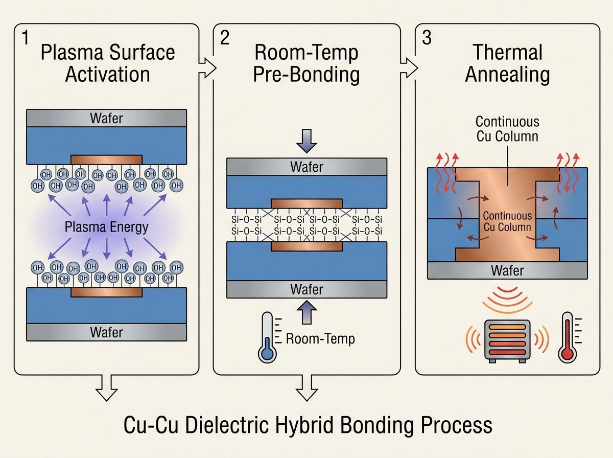
Step 1: Dielectric Plasma Activation    Step 2: Room-Temp Pre-Bonding      Step 3: Thermal Annealing
      (Surface Cleaning)                     (Van der Waals Seals)             (Atomic Cu Diffusion)

      OH  OH  OH  OH                         Si-O-H ... H-O-Si                 Si--O--Si  Covalent Bond
   +-------------------+                  +---------------------+            +-----------------------+
   |    Dielectric     |                  |     Dielectric      |            |      Dielectric       |
   +-------------------+                  +---------------------+            +-----------------------+
   |   Recessed Cu     |                  |  Recessed Cu Gap    |            | Expanded Cu Interface |
   +-------------------+                  +---------------------+            +-----------------------+
Surface Activation & Chemical Preparation
Before bonding, polished surfaces containing dielectric material (SiO2 or SiCN) and flush copper pads undergo nitrogen or argon plasma activation. Plasma treatment removes surface contaminants and terminates the dielectric surface with hydrophilic hydroxyl groups (-OH).
Step 1: Room-Temperature Dielectric Fusion
Alignment: Optical alignment systems align opposing dies or wafers with sub-micron placement accuracy.
Contact: The surfaces are brought together at room temperature without applying external pressure.
Van der Waals Bonding: Hydroxyl groups on opposing surfaces spontaneously form hydrogen bonds across the interface.
Covalent Polymerization: Water molecules desorb from the interface, converting hydrogen bonds into strong covalent siloxane (Si-O-Si) or silicon-nitride bonds. This seals the dielectric interface and seals embedded copper pads within a gas-tight cavity before heating begins.
Step 2: Thermal Annealing & Solid-State Copper Diffusion
Once the dielectric seal forms, the assembly undergoes post-bond thermal annealing at temperatures between 150°C and 300°C.
The Differential Expansion Mechanism: Copper possesses a higher Coefficient of Thermal Expansion (CTE) (≈ 16.5 × 10⁻⁶/K) than surrounding silicon dioxide (≈ 0.5 × 10⁻⁶/K) or silicon carbonitride.
Closing the CMP Recess: During Chemical Mechanical Planarization (CMP), copper pads are deliberately polished to a slight sub-nanometer concave recess (2–5 nm). As the temperature rises during annealing, the thermal expansion of copper exceeds that of the surrounding oxide, filling the recess gap and forcing opposing Cu pads into firm contact.
Solid-State Atomic Diffusion: Under contact pressure caused by thermal expansion, copper atoms cross the interface via solid-state interdiffusion. Recrystallization merges opposing metallic pads into continuous single-crystal copper columns.
Performance Payoff: Signal Integrity & Memory Bandwidth Scaling
Eliminating physical solder bumps resolves key electrical bottlenecks in memory-to-logic and logic-to-logic packaging architectures, enabling performance improvements across AI chiplets and high-performance computing (HPC) nodes.
Why Hybrid Bonding is the Future of Packaging
       Interconnect Density Scaling (Pads/mm²)
  1,000,000 +----------------------------------+ Hybrid Bonding
            |                                  | (0.8µm - 9µm)
    100,000 +----------------------------------+
            |
     10,000 +----------------------------------+ TCB Microbumps
            |                                  | (10µm - 25µm)
      1,000 +----------------------------------+ Mass Reflow
            +----------------------------------+ (35µm+)
Electrical Signal Integrity Improvements
Sub-Femtofarad Parasitic Capacitance: Shrinking the inter-die vertical gap to zero drops parasitic capacitance to sub-femtofarad levels (<0.2 fF)[3]. This reduces capacitive loading, widens eye diagram openings, and cuts high-frequency insertion losses.
Lower Interconnect Resistance: Direct metallic contact eliminates high-resistivity tin-based solders and intermetallic compounds. This lowers connection resistance, improving power integrity and reducing I2R power losses across massive vertical power delivery networks.
Reduced Energy-per-Bit: Because short interconnect paths minimize parasitic inductance and capacitance, the energy required to transmit a single bit across dies drops significantly compared to conventional microbump interfaces.
Memory Bandwidth Scaling in HBM Architectures
High-bandwidth memory depends on thousands of vertical Through-Silicon Vias (TSVs) to drive wide parallel memory buses. As AI workloads push memory requirements higher, hybrid bonding helps expand these interfaces:
Expanding Parallel Buses: Advanced architectures like JEDEC HBM4 double the interface bus width from 1024-bit to 2048-bit, targeting single-stack transfer rates of 2.0–2.8 TB/s. Fitting tens of thousands of TSV connections within a standard die footprint requires reducing interconnect pitches below 10 μm—a density threshold achievable via hybrid bonding.
Real-World High-Density Implementations: Commercial deployments demonstrate the performance impact of this technology. AMD’s implementation of TSMC SoIC-X hybrid bonding (9 μm pitch) in 3D V-Cache processors demonstrated a multi-hundred-fold interconnect density increase and a more than 10x improvement in interconnect energy efficiency compared to microbump chiplet designs.
Manufacturing Realities: Planarization, Particle Defectivity, and Thermal Risks
While hybrid bonding offers clear electrical advantages, high-volume manufacturing faces strict physical tolerances, low defect margins, and unique thermal challenges.
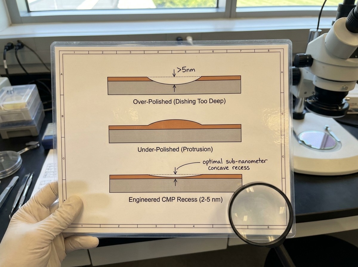
            CMP Surface Profile Control

    [X] Over-Polished (Dishing Too Deep)
    +---+                   +---+
    |   |___ Concave _______|   |  <- Cu expansion cannot bridge gap
    +---------------------------+

    [X] Under-Polished (Protrusion)
    +---+   +-----------+   +---+
    |   |---| Convex    |---|   |  <- Prevents dielectric contact
    +---------------------------+

    [OK] Engineered CMP Recess (2 - 5 nm)
    +---+                   +---+
    |   |-- Sub-nm Recess --|   |  <- Perfect CTE closure during anneal
    +---------------------------+
1. CMP Planarization & Copper Dishing Control
Chemical Mechanical Planarization (CMP)[4] is a critical step in hybrid bonding process flows.
The Mechanics of Dishing: Soft copper polishes faster than hard surrounding dielectric oxide. Excessive polishing creates concave "dishing" across the copper pad[6].
Sub-Nanometer Tolerances: Surface roughness must be maintained at Rq ≤ 0.1–0.2 nm. If copper dishing exceeds 5 nm, thermal expansion during annealing will fail to bring the metal pads into contact, creating internal micro-voids. Conversely, if copper protrudes above the dielectric, it prevents room-temperature dielectric pre-bonding.
2. Particle Sensitivity & Cleanroom Standards
Because room-temperature dielectric bonding relies on Van der Waals contact, surface contamination is a primary yield killer.
Amplified Void Size: A single microscopic particle larger than 100 nm trapped at the interface prevents dielectric contact across a surrounding area thousands of times its physical size, creating a large unbonded void.
Transition to Plasma Dicing: Traditional mechanical blade dicing or laser ablation generates silicon debris that ruins surface planarization. To prevent contamination, packaging lines use plasma dicing (dry etching along pre-patterned dicing streets) and operate within ISO 3 (Class 1) cleanroom environments.
3. Thermal Impedance in Stacked Oxide Structures
Dielectric materials like SiO2 exhibit lower thermal conductivity (~1.3 W/m·K) compared to metals like copper (~390 W/m·K) or bulk silicon (~148 W/m·K). Stacking multiple dies bound by thick oxide layers can trap heat in active logic regions.
To prevent thermal throttling, chip architects use higher-conductivity dielectrics (such as silicon carbonitride, SiCN), re-architect floorplans (e.g., placing cache underneath active compute logic), or integrate structural silicon heat-sink paths.
4. Wafer Thinning and Warpage Control
Exposing Through-Silicon Vias requires grinding wafers down to under 50 μm. At these thicknesses, silicon wafers lose structural rigidity and warp easily under thermal stress. Uncontrolled warpage exceeding 100 μm causes lateral overlay misalignment (>100 nm) during bonding, causing pad-to-pad offsets or delamination. Handling thinned wafers requires rigid temporary carrier systems throughout processing.
Industry Gaps & Disagreements in Advanced Packaging Benchmarks
Discussions around 3D packaging often oversimplify adoption timelines, manufacturing capabilities, and integration methods.
Myth 1: "Hybrid bonding will immediately render microbumps obsolete."
Reality: Microbumps will remain a primary interconnect technology for years to come. Cost considerations dictate a tiered approach: microbumps and thermo-compression bonding remain cost-effective for standard 2.5D interposers, mature SiPs, and consumer GPUs, whereas hybrid bonding targets ultra-dense logic-on-logic stacks (e.g., 3D V-Cache) and 16-Hi+ HBM memory stacks.
Myth 2: "Sub-micron pitch is ubiquitous across commercial manufacturing today."
Reality: Sub-micron pitches (<0.5 μm) have been proven in research environments and wafer-to-wafer roadmaps. However, commercial high-volume manufacturing currently operates primarily in the 0.8 μm – 9 μm pitch range due to yield management and alignment equipment constraints.
Myth 3: "Wafer-to-Wafer (W2W) bonding fits all heterogeneous architectures."
Reality: W2W provides high throughput and precision, but requires both top and bottom dies to be identical in physical size, with high silicon yield across both wafers. Heterogeneous architectures with mismatched die sizes (such as pairing small cache dies with large logic dies) rely on Chip-to-Wafer (C2W) bonding using temporary carrier wafers, which adds processing steps and die-placement complexity.
Engineering Checklist for Advanced 3D Packaging Design
This checklist outlines core design verification steps for packaging engineering and chiplet integration teams transitioning to hybrid bonding:
Interconnect Density Evaluation: Is the required I/O pitch below 10 μm or interconnect density above 10,000 pads/mm2? (If pitch >15 μm, evaluate TCB or microbumps first to reduce processing cost).
Integration Topology Selection: Choose between Wafer-to-Wafer (W2W) for identical die sizes with high wafer yields, or Chip-to-Wafer (C2W) for mismatched die sizes requiring Known Good Die (KGD) pre-sorting.
CMP Recess Profile Control: Confirm that post-CMP copper dishing tolerances are maintained between 2 nm and 5 nm across the wafer, with surface roughness Rq ≤ 0.2 nm.
Particle Contamination Prevention: Specify plasma dicing over mechanical blade dicing for singularization, and verify assembly line compliance with ISO 3 (Class 1) standards.
Thermal Barrier Modeling: Run 3D thermal simulations to confirm dielectric layers (SiO2/SiCN) do not cause active junction temperatures (Tj) to exceed operational limits under peak power loads.
Carrier Support & Warpage Budget: Establish temporary bonding and debonding (TBDB) support carriers to keep overall wafer warpage below 100 μm for thinned dies (<50 μm).
Sourcing Specialty ICs and Advanced Packaging Materials via UTMEL
Transitioning to advanced 3D packaging requires secure component supply chains, specialized substrate materials, and high-purity silicon interposers. When implementing complex heterogeneously integrated systems, engineering teams face challenges with component allocations, long lead times, and sourcing verified silicon dies.
As an electronic component distributor, UTMEL helps engineering and procurement teams navigate these supply chain demands. UTMEL provides access to active semiconductors, power management ICs, memory modules, and specialty passive components needed to build modern system-in-package solutions.
To learn more about foundational packaging techniques and how the industry has evolved from wire bonding to multi-die integration, read UTMEL's guide on the Introduction to IC Packaging. For broader insights into how leading foundries are pushing process node scaling to support next-generation compute architectures, explore UTMEL's coverage on how Intel CEO Reiterates 2024 Will Achieve Process Leadership.
Frequently Asked Questions (FAQ)
What is the primary difference between hybrid bonding and fusion bonding?
Fusion bonding joins two dielectric surfaces (such as SiO2-SiO2) to create a structural bond without electrical interconnections, commonly used in backside-illuminated (BSI) image sensors. Hybrid bonding concurrently bonds both dielectric surfaces and embedded metal contacts (Cu-Cu), providing simultaneous structural adhesion and vertical electrical connectivity across the interface.
Why can't traditional solder reflow achieve a sub-micron pitch?
Liquid solder exhibits surface tension during thermal reflow, causing the solder droplet to bulge outward. When pitch scales below 10 μm, the lateral expansion of liquid solder exceeds the spacing between pads, causing solder bridging and electrical short circuits.
How does thermal expansion drive the Cu-Cu bonding process?
During post-bond thermal annealing (150°C–300°C), copper expands faster than the surrounding dielectric matrix due to its higher Coefficient of Thermal Expansion (CTE). This expansion forces the pre-recessed copper pads outward to close sub-nanometer CMP gaps, creating metal-to-metal contact pressure that drives solid-state atomic copper diffusion.
Is Wafer-to-Wafer (W2W) or Chip-to-Wafer (C2W) better for 3D packaging?
Wafer-to-Wafer (W2W) offers higher throughput, superior alignment accuracy, and lower contamination risks, but requires both wafers to have identical die footprints and high yields. Chip-to-Wafer (C2W) accommodates mismatched die sizes and allows Known Good Die (KGD) pre-sorting to preserve compound yield, making it better suited for heterogeneous AI chiplet architectures.
Sources and references used for this guide
Bumps Vs. Hybrid Bonding For Advanced Packaging
Source type: reputable professional source
Used for: Context on microbump scaling limits and the 10-micron wall.
Caution: Industry publication; not a peer-reviewed physics paper.Research progress of hybrid bonding technology for three-dimensional integration
Source type: research source
Used for: Cu-Cu bonding mechanisms and solid-state diffusion physics.Hybrid Bonding Plays Starring Role in 3D Chips
Source type: reputable professional source
Used for: Electrical and thermal performance benefits in 3D integration.Challenges and Innovations in Chemical Mechanical Planarization
Source type: research source
Used for: CMP dishing and planarization realities.Void-free Cu/dielectric hybrid bonding at low-temperature
Source type: research source
Used for: Sub-micron pitch scaling potential.
Caution: Demonstrates capability, not necessarily high-volume manufacturing standard.A Review of the Cu Chemical Mechanical Planarization
Source type: research source
Used for: Manufacturing friction points and CMP challenges.
 UTMEL
UTMEL
We are the professional distributor of electronic components, providing a large variety of products to save you a lot of time, effort, and cost with our efficient self-customized service. careful order preparation fast delivery service
 Improving the Energy Conversion Efficiency of Triboelectric NanogeneratorsSaumitra Jagdale19 November 20243256
There is a huge growth in demand for self-sustaining electronic devices, as the traditional power-generating devices fail in remote and harsh environments due to the periodic requirement of battery changes. Also, these devices are frequency specific; some work only in high frequency and some in low frequency. Triboelectric nanogenerators (TENGs) provide a promising solution by efficiently converting mechanical energy into electricity as they are versatile, compact, and cheap, making them a popular choice.
Read More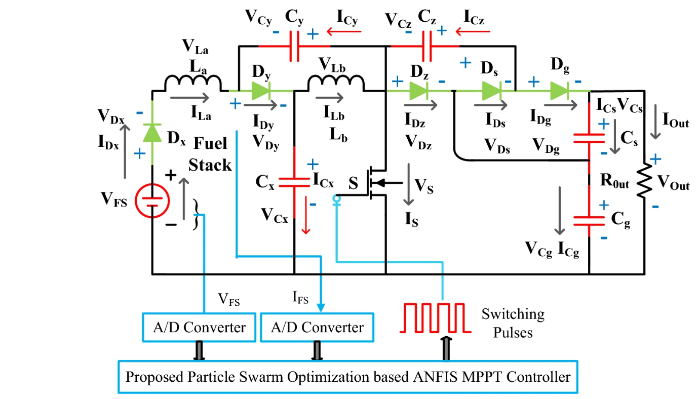 Methodologies for Increasing Efficiency of Fuel Stack Technology for Energy GenerationSaumitra Jagdale19 November 20243102
Presently, power companies are moving towards renewable energy systems. Conventional energy sources are more expensive because they require a vast network to be maintained and huge human resources. Also, they harm the environment by releasing several harmful gases. As the industry’s focus shifts toward renewable energy sources, energy systems powered by Proton Exchange Membrane Fuel Stacks (PEMFS) are gaining traction.
Read More VSC Light Meaning, Causes, and Step-by-Step DiagnosticsUTMEL19 May 20263489
A VSC (Vehicle Stability Control) light indicates the system is disabled, often as a fail-safe triggered by unrelated engine faults like a loose gas cap. While the stability system prevents lateral skidding, it shuts down when sensor data is unreliable. Proper diagnosis requires an ABS-capable OBD2 scanner. Resolving the root engine code, checking wheel speed sensors, or performing a zero-point calibration usually restores system function.
Read More What JEDEC JEP203 and JEP204 Actually Change for SiC Qualification Engineers and Component BuyersUTMEL29 July 2026481
Summary: When JEDEC published JEP203 and JEP204 on June 3, 2026[1], most coverage treated them as an announcement. They are better understood as the first shared language the silicon carbide industry has had for two problems that have quietly consumed engineering hours since the first commercial SiC MOSFETs shipped: short-circuit evaluation that produces numbers you can compare across suppliers, and a consolidated reference of stress procedures so qualification engineers stop reinventing test plans from scratch. This article explains what changes on Monday morning and what to ask suppliers for now.
Read More 2nm vs 3nm Chips: What the Latest Process Nodes Mean for PerformanceUTMEL19 August 20261570
The shift from 3nm to 2nm process nodes marks a fundamental change in transistor architecture, moving from FinFET to Gate-All-Around (GAA) nanosheets. This transition delivers meaningful improvements in performance, power, and density, but also introduces new challenges like SRAM scaling limits, thermal density, and backside power delivery. The article compares TSMC, Samsung, and Intel approaches, offering a practical decision framework for engineering teams.
Read More
Subscribe to Utmel !


