How a CPU is made? [HD Graphics]

How a CPU is made
2026 Executive Summary: How CPUs Are Made
The core of CPU manufacturing is Photolithography using Extreme Ultraviolet (EUV) light. Starting with 99.9999% pure electronic-grade silicon derived from sand, manufacturers process 300mm wafers through hundreds of steps. As of January 2026, the industry standard has moved to Angstrom-era nodes (2nm/18A), utilizing Gate-All-Around (GAA) transistor architecture to fit over 50 billion transistors onto a single consumer chip. This guide covers the end-to-end process from silicon ingot to packaged processor.
The CPU, often referred to as the "brain" or "microprocessor," serves as the computational engine of modern computers and AI systems. As of 2026, the complexity of these chips has skyrocketed, with specifications and clock speeds acting as critical benchmarks for performance in PCs, data centers, and edge devices. The Intel x86 architecture has now evolved over nearly five decades, and modern iterations (along with ARM and RISC-V) continue to drive the digital economy.

The transistor remains the fundamental building block of the CPU. To increase processing power in 2026, engineers must fit billions of transistors into a chip no larger than a fingernail. Because these components are now measured in Angstroms (0.1 nanometers), human hands cannot assemble them; they are manufactured using advanced robotic photolithography.
A transistor is essentially a microscopic binary switch: on (1) or off (0). While early computers used vacuum tubes, today's Angstrom-era chips contain logic gates that switch billions of times per second. In this detailed guide, we will walk you through the sophisticated fabrication process of a Central Processing Unit, transforming a pile of silicon sand into a powerful integrated circuit.
1. What are the raw materials for modern CPUs?
The primary raw material for CPUs is silicon, extracted from silica sand (silicon dioxide). While it seems improbable that high-performance AI processors originate from common sand, the secret lies in the purification process. Manufacturers cannot use standard beach sand; they must extract and purify silicon to an "Electronic Grade" purity of 99.9999% (often called "nine nines"). If the silicon substrate is not perfectly pure, the electrons cannot flow efficiently, rendering the high-performance processor useless.

Beyond silicon, modern CPUs utilize a complex stack of metals and rare earth elements. While aluminum was used historically, copper is the standard for interconnects due to its superior conductivity, though 2026 processes are now integrating Cobalt and Ruthenium for the smallest connections to prevent electromigration. Electromigration occurs when high-speed electrons physically displace atoms in the wire, creating voids (open circuits) or hillocks (short circuits), which can permanently destroy a chip's logic.
2. Silicon Purification and Ingot Creation
Before chip fabrication begins, the raw silicon must be transformed into a single crystal structure. The purified silicon is melted in a quartz crucible at temperatures exceeding 1,400°C (2,500°F). To ensure the necessary electronic properties, a "seed crystal" is lowered into the melt and slowly rotated and pulled upward.

This process, known as the Czochralski method, produces a cylindrical ingot of monocrystalline silicon. As of 2026, the industry standard for these ingots is 300mm (12 inches) in diameter. The internal atomic structure must be perfectly aligned to allow electron flow.
Once the ingot is formed, it is sliced into wafers approximately 0.7mm thick. These wafers are polished to a mirror-perfect finish; any surface imperfection larger than a few nanometers can ruin the final circuitry. Intel and TSMC invest billions in fabrication plants ("fabs") capable of handling these 300mm wafers, as larger wafers allow for more chips to be produced simultaneously, reducing the cost per unit.
3. Photolithography and EUV Technology
Photolithography is the process of printing circuit patterns onto the silicon wafer using light. In the 2026 manufacturing landscape, this is achieved using Extreme Ultraviolet (EUV) lithography. A photosensitive chemical called "photoresist" is spun onto the wafer. The wafer is then exposed to deep ultraviolet light passed through a "mask" (stencil) that contains the circuit blueprint.
This step is incredibly complex because the features being printed are smaller than the wavelength of visible light.
Wavelength: Modern High-NA EUV systems use light with a wavelength of just 13.5 nanometers.
Precision: The precision required is equivalent to hitting a golf ball into a specific hole on the moon.
Complexity: A modern CPU requires over 50 to 80 separate masking layers to build the 3D structure of the transistors.

When the light hits the photoresist, it changes the chemical solubility of the exposed areas. These areas are then washed away, revealing the silicon dioxide or substrate underneath, ready for etching.
4. Doping and Ion Implantation
Doping is the process of bombarding exposed silicon areas with ions to alter their electrical conductivity. After the photolithography creates the pattern, the wafer is subjected to ion implantation. Atoms such as Boron or Phosphorus are shot into the silicon lattice at high speeds.
This transforms the silicon from an insulator into a semiconductor. This creates the N-type (negative) and P-type (positive) regions essential for the transistor's function.
2026 Technology Note: While older chips used planar (flat) transistors, modern CPUs use GAA (Gate-All-Around) or RibbonFET technology. In this architecture, the "gate" surrounds the channel on all four sides, allowing for superior control over power leakage and enabling higher performance at lower voltages.
5. Interconnects and Layering
Once the transistors are formed on the silicon base, they must be wired together. This is done by building layers of metal interconnects above the transistors.
Insulation: Dielectric materials are added to separate the layers.
Vias: Tiny vertical holes are etched and filled with metal to connect different layers.
Scale: A modern processor may have over 15 to 20 layers of metal wiring.
The resulting structure looks like a multi-story highway system, where signals travel between billions of transistors at the speed of light.
6. Testing, Binning, and Packaging
After the fabrication on the wafer is complete, the individual dies are tested while still on the silicon disk. This is known as "wafer sort." Probes apply voltage to check for defects.

The wafer is then sliced into individual chips (dies) using diamond saws or lasers. Functional dies are packaged—mounted onto a green substrate and covered with a heat spreader (IHS).
The Binning Process: Not all chips are created equal. Due to microscopic variations in the manufacturing process, some chips perform better than others.
High Bin: Chips that remain stable at high voltages and frequencies are labeled as premium models (e.g., Core Ultra 9 or Ryzen 9).
Mid/Low Bin: Chips with slight imperfections or lower efficiency are locked to lower speeds and sold as mid-range or budget processors (e.g., Core Ultra 5).
Disabled Cores: If a specific core is defective, it is permanently disabled, and the chip is sold as a model with fewer cores.
This maximizes yield and reduces waste, explaining why a single production line produces multiple CPU models.
7. Visual Step-by-Step Guide (From Sand to Chip)
Note: The following diagrams illustrate the foundational Intel manufacturing workflow. While modern 2026 techniques (like GAAFET and High-NA EUV) are more complex, the fundamental stages remain consistent.
Step 1: Sand Collection. Silicon is the second most prevalent element in the Earth's crust. Deoxygenated sand (quartz) contains up to 25% silicon.

Step 2: Silicon Smelting. Sand is purified into Electronic Grade Silicon (EGS) with less than one impurity atom per billion silicon atoms.

Step 3: Ingot Formation. The result is a monocrystalline ingot, weighing approx 100kg with 99.9999% purity.

Step 4: Wafer Slicing. The ingot is sliced into thin 300mm wafers and polished to a mirror finish.

Step 5: Photoresist Application. A blue photosensitive liquid is spun onto the wafer surface.

Step 6: Photolithography Exposure. UV light passes through a stencil (mask) to project the circuit design onto the wafer, shrinking the pattern by 4x.

Step 7: Etching. Chemicals dissolve the exposed soft photoresist and etch away the silicon oxide substrate to create channels.

Step 8: Ion Implantation. The silicon is bombarded with ions to create conductive N/P regions.

Step 9: Copper Electroplating. Copper is deposited into the etched trenches to create the transistors' electrical connections.

Step 10: Polishing & Interconnects. Excess copper is polished off, and multiple metal layers are built up to connect transistors.

Step 11: Wafer Slicing & Sort. The wafer is cut into individual dies. Defective dies are discarded.

Step 12: Final Packaging. The functional die is mounted on a substrate and covered with a heat spreader.

Frequently Asked Questions about CPU Manufacturing
1. What does the "nanometer" (nm) process node mean in 2026?
Originally, this referred to the actual size of the transistor gate. In 2026, terms like "2nm" or "18A" (Angstrom) are marketing terms indicating generation density and efficiency rather than exact physical dimensions. A smaller number implies higher transistor density, better power efficiency, and faster performance.
2. Why are modern CPUs so expensive?
The cost is driven by the astronomical investment required for fabrication. A modern fab costs over $20 billion to build. The EUV lithography machines alone cost upwards of $350 million each. Additionally, the process involves thousands of steps, and a single mistake can ruin months of work, resulting in "yield loss" that drives up the price of successful chips.
3. Why use Copper instead of Silver?
While silver is slightly more conductive, it oxidizes rapidly and is prone to migration problems. Copper (and now Cobalt for tiny layers) offers the best balance of conductivity, reliability, and cost. Modern contacts are often gold-plated to prevent corrosion at the connection points.
4. How long does it take to make a single CPU?
From the moment a raw silicon wafer enters the fab to the time it is packaged as a finished CPU, the process takes approximately 3 to 4 months.
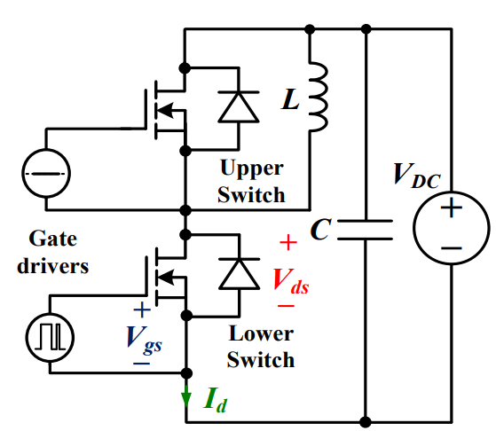
 Discovering New and Advanced Methodology for Determining the Dynamic Characterization of Wide Bandgap DevicesSaumitra Jagdale15 March 20242471
For a long era, silicon has stood out as the primary material for fabricating electronic devices due to its affordability, moderate efficiency, and performance capabilities. Despite its widespread use, silicon faces several limitations that render it unsuitable for applications involving high power and elevated temperatures. As technological advancements continue and the industry demands enhanced efficiency from devices, these limitations become increasingly vivid. In the quest for electronic devices that are more potent, efficient, and compact, wide bandgap materials are emerging as a dominant player. Their superiority over silicon in crucial aspects such as efficiency, higher junction temperatures, power density, thinner drift regions, and faster switching speeds positions them as the preferred materials for the future of power electronics.
Read More A Comprehensive Guide to FPGA Development BoardsUTMEL11 September 202514694
This comprehensive guide will take you on a journey through the fascinating world of FPGA development boards. We’ll explore what they are, how they differ from microcontrollers, and most importantly, how to choose the perfect board for your needs. Whether you’re a seasoned engineer or a curious hobbyist, prepare to unlock new possibilities in hardware design and accelerate your projects. We’ll cover everything from budget-friendly options to specialized boards for image processing, delve into popular learning paths, and even provide insights into essential software like Vivado. By the end of this article, you’ll have a clear roadmap to navigate the FPGA landscape and make informed decisions for your next groundbreaking endeavor.
Read More Applications of FPGAs in Artificial Intelligence: A Comprehensive GuideUTMEL29 August 20253607
This comprehensive guide explores FPGAs as powerful AI accelerators that offer distinct advantages over traditional GPUs and CPUs. FPGAs provide reconfigurable hardware that can be customized for specific AI workloads, delivering superior energy efficiency, ultra-low latency, and deterministic performance—particularly valuable for edge AI applications. While GPUs excel at parallel processing for training, FPGAs shine in inference tasks through their adaptability and power optimization. The document covers practical implementation challenges, including development complexity and resource constraints, while highlighting solutions like High-Level Synthesis tools and vendor-specific AI development suites from Intel and AMD/Xilinx. Real-world applications span telecommunications, healthcare, autonomous vehicles, and financial services, demonstrating FPGAs' versatility in mission-critical systems requiring real-time processing and minimal power consumption.
Read More 800G Optical Transceivers: The Guide for AI Data CentersUTMEL24 December 20253838
The complete guide to 800G Optical Transceiver standards (QSFP-DD vs. OSFP). Overcome supply shortages and scale your AI data center with Utmel Electronic.
Read More Xilinx FPGAs: From Getting Started to Advanced Application DevelopmentUTMEL09 September 20254299
This guide is your comprehensive roadmap to understanding and mastering the world of Xilinx FPGA technology. From selecting your first board to deploying advanced AI applications, we'll cover everything you need to know to unlock the potential of these remarkable devices. The global FPGA market is on a significant growth trajectory, expected to expand from USD 8.37 billion in 2025 to USD 17.53 billion by 2035. This surge is fueled by the relentless demand for high-performance, adaptable computing in everything from 5G networks and data centers to autonomous vehicles and the Internet of Things (IoT). This guide will walk you through the key concepts, tools, and products in the Xilinx ecosystem, ensuring you're well-equipped to be a part of this technological revolution.
Read More
Subscribe to Utmel !
![ATAES132A-MAHER-T]() ATAES132A-MAHER-T
ATAES132A-MAHER-TMicrochip Technology
![TLE8263EXUMA1]() TLE8263EXUMA1
TLE8263EXUMA1Infineon Technologies
![HCS365/P]() HCS365/P
HCS365/PMicrochip Technology
![HCS200/P]() HCS200/P
HCS200/PMicrochip Technology
![DLPA2005ERSLR]() DLPA2005ERSLR
DLPA2005ERSLRTexas Instruments
![ATSHA204-SH-CZ-T]() ATSHA204-SH-CZ-T
ATSHA204-SH-CZ-TMicrochip Technology
![SN74AVC6T622PWR]() SN74AVC6T622PWR
SN74AVC6T622PWRTexas Instruments
![MOC3061VM]() MOC3061VM
MOC3061VMON Semiconductor
![PAM8904JPR]() PAM8904JPR
PAM8904JPRDiodes Incorporated
![AD9961BCPZRL]() AD9961BCPZRL
AD9961BCPZRLAnalog Devices Inc.


 Product
 Brand
Brand Articles
 Tools
Tools


