Product
 Brand
Brand Articles
 Tools
Tools
This New Material Promises to Be the Best Semiconductor
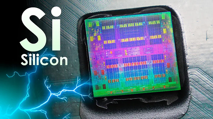
Silicon - The Smartest Element on Earth!
Silicon is one of the most abundant elements on the planet and in its pure form has become the basis for many modern technologies, from solar cells to computer chips. But silicon's properties as a semiconductor are far from ideal.
For one thing, although silicon allows electrons to pass easily through its structure, it is not well suited to "holes" - the positively charged counterpart of electrons - and the use of both is important for certain types of chips. Important. More importantly, silicon is not very good at conducting heat, which is why overheating problems and expensive cooling systems are common in computers.

Now, a group of researchers at MIT, the University of Houston, and other institutions have conducted experiments showing that a material called cubic boron arsenide overcomes both of these limitations. It provides high mobility for electrons and holes and has excellent thermal conductivity. The researchers say it is the best semiconductor material ever discovered, perhaps the best one.
Until now, cubic arsenide has only been fabricated and tested in small, non-uniform lab-scale batches. The researchers had to use a special method originally developed by former MIT postdoctoral fellow Bai Song to test small areas in the material. More work is needed to determine whether cubic boron arsenide can be manufactured in a practical, economical form, let alone replace the ubiquitous silicon. But even in the near future, the researchers say, the material could find some uses where its unique properties could have a significant impact.
The findings, published today in the journal Science, were authored by Jungwoo Shin, a postdoctoral fellow at MIT, and Gang Chen, a professor of mechanical engineering at MIT. Participants also included Zhifeng Ren of the University of Houston and 14 others from MIT, the University of Houston, the University of Texas at Austin, and Boston College.
Earlier studies, including work by David Broido, co-author of the new paper, predicted theoretically that the material would have high thermal conductivity. Subsequent work proved this prediction experimentally. This latest work completes the analysis by experimentally confirming a prediction made by Chen's team back in 2018: cubic boron arsenide also has very high mobility for electrons and holes, "which makes this material very unique," Chen says.
.jpg")
Earlier experiments had shown that the thermal conductivity of cubic boron arsenide was almost 10 times that of silicon. "So this is very attractive for heat dissipation," says Chen. They also showed that the material has a very good band gap, a property that gives it great potential as a semiconductor material.
This new work now fills in that picture, showing that boron arsenide has high electron and hole mobility and has all the key qualities needed for an ideal semiconductor. "This is important because of course in semiconductors we have both positive and negative charges. So if you make a device, you want a material where both electrons and holes propagate with less resistance," says Chen.
Silicon has good electron mobility but poor hole mobility, while other materials, such as gallium arsenide, which is widely used in lasers, also have good electron mobility but not good mobility for holes.
"Heat is now a major bottleneck for many electronics," said Shin, lead author of the paper. "Silicon carbide is replacing silicon for power electronics in major electric vehicle industries, including Tesla because it has three times the thermal conductivity of silicon despite lower electron mobility. Imagine what can be achieved with boron arsenide, which has thermal conductivity and mobility 10 times higher than silicon. It could be a game changer."
Shin added that "the key milestone that made this discovery possible was the advancement of the MIT ultrafast laser grating system," originally developed by Song. Without this technology, he said, it would not have been possible to demonstrate the material's high mobility for electrons and holes.
The electronic properties of cubic boron arsenide were initially predicted based on quantum mechanical density functional calculations done by Chen's group, he said, and these predictions have now been verified by experiments conducted at MIT using optical detection of samples made by Ren and members of his team at the University of Houston.
The researchers say the material has the best thermal conductivity of any semiconductor and the third best thermal conductivity of all materials - after diamond and isotope-rich cubic boron nitride. "Now, we have also predicted the quantum mechanical behavior of electrons and holes from first principles, which also proved to be correct," Chen said.
.png")
"This is impressive because I don't actually know of any other material with all these properties other than graphene," he said. "It's a bulk material with those properties."
The challenge now, he says, is to find practical ways to bring this material to usable quantities. Current methods of making very inhomogeneous materials mean that the team must find ways to test the material in small localized patches that are uniform enough to provide reliable data. While they have demonstrated the material's great potential, "we don't know if or where it will actually be used," says Chen.
"Silicon is the mainstay of the whole industry," Chen says. "So, OK, we have better material, but is it really going to offset the industry? We don't know." While the material appears to be almost an ideal semiconductor, "whether it can actually get into devices and replace some of the current markets, I think that's yet to be proven."
While the thermal and electrical properties have proven to be excellent, many other properties of the material remain to be tested, such as its long-term stability, says Chen. "There are many other factors that we don't yet know about to make the device."
He adds, "It could be so important that people haven't even really looked at this material." Now that the desirable properties of boron arsenide have become clearer, suggesting that the material is "in many ways the best semiconductor," he says, "perhaps this material will get more attention."
For commercial use, Ren says, "A huge challenge is to produce and purify cubic boron arsenide as efficiently as silicon. ...... It took decades for silicon to win the crown, with a purity of over 99.99999999%, or '10 nines' for mass production today."
To make it practical in the marketplace, Chen said, "more people really need to develop different ways to make and characterize better materials." It remains to be seen whether the funding needed for such developments will be available, he said.
The research was supported by the US Office of Naval Research and used the facilities of the MIT MRSEC Shared Experimentation Facility, with support from the National Science Foundation.
Related News
1、Chip Packaging Lead Time Has Grown to 50 Weeks
2、Eight Internet of Things (IoT) Trends for 2022
3、Demand for Automotive Chips Will Surge 300%
4、Volkswagen CFO: Chip Supply Shortage Will Continue Until 2024
5、BMW CEO: The Car Chip Problem Will Not Be Solved Until 2023
6、Shenzhen: This Year Will Focus on Promoting SMIC and CR Micro 12-inch Project
 UTMEL
UTMEL
We are the professional distributor of electronic components, providing a large variety of products to save you a lot of time, effort, and cost with our efficient self-customized service. careful order preparation fast delivery service
 UTMEL 2024 Annual gala: Igniting Passion, Renewing BrillianceUTMEL18 January 20244856
As the year comes to an end and the warm sun rises, Utmel Electronics celebrates its 6th anniversary.
Read More Electronic Components Distributor Utmel to Showcase at 2024 IPC APEX EXPOUTMEL10 April 20245851
Utmel, a leading electronic components distributor, is set to make its appearance at the 2024 IPC APEX EXPO.
Read More Electronic components distributor UTMEL to Showcase at electronica ChinaUTMEL07 June 20244435
The three-day 2024 Electronica China will be held at the Shanghai New International Expo Center from July 8th to 10th, 2024.
Read More Electronic components distributor UTMEL Stands Out at electronica china 2024UTMEL09 July 20244808
From July 8th to 10th, the three-day electronica china 2024 kicked off grandly at the Shanghai New International Expo Center.
Read More A Combo for Innovation: Open Source and CrowdfundingUTMEL15 November 20195376
Open source is already known as a force multiplier, a factor that makes a company's staff, financing, and resources more effective. However, in the last few years, open source has started pairing with another force multiplier—crowdfunding. Now the results of this combination are starting to emerge: the creation of small, innovative companies run by design engineers turned entrepreneurs. Although the results are just starting to appear, they include a fresh burst of product innovation and further expansion of open source into business.
Read More
Subscribe to Utmel !
![PT10LV10-305A3030]() PT10LV10-305A3030
PT10LV10-305A3030Amphenol Piher Sensing Systems
![PT15NV15-473A2020-I-PM-S]() PT15NV15-473A2020-I-PM-S
PT15NV15-473A2020-I-PM-SAmphenol Piher Sensing Systems
![PT15NV17-102A2020-I-PM-S]() PT15NV17-102A2020-I-PM-S
PT15NV17-102A2020-I-PM-SAmphenol Piher Sensing Systems
![PT15NH05-474A2020-I-PM-S]() PT15NH05-474A2020-I-PM-S
PT15NH05-474A2020-I-PM-SAmphenol Piher Sensing Systems
![PT15NV17-104A2020-I-PM-S]() PT15NV17-104A2020-I-PM-S
PT15NV17-104A2020-I-PM-SAmphenol Piher Sensing Systems
![PT15NH05-473A2020-I-PM-S]() PT15NH05-473A2020-I-PM-S
PT15NH05-473A2020-I-PM-SAmphenol Piher Sensing Systems
![PT10MV10-472A2020-I-PM-S]() PT10MV10-472A2020-I-PM-S
PT10MV10-472A2020-I-PM-SAmphenol Piher Sensing Systems
![PT10LH01-505A2020]() PT10LH01-505A2020
PT10LH01-505A2020Amphenol Piher Sensing Systems
![PT10KV10-104A2020-PM-S]() PT10KV10-104A2020-PM-S
PT10KV10-104A2020-PM-SAmphenol Piher Sensing Systems
![PT10MH01-223A2020-I-PM-S]() PT10MH01-223A2020-I-PM-S
PT10MH01-223A2020-I-PM-SAmphenol Piher Sensing Systems