
 Product
 Brand
Brand Articles
 Tools
Tools
AD620 Instrumentation Amplifier: Pinout, Schematic and Price

18mA per Channel 500pA 93 dB Instrumentational OP Amps 36V 4.6V~36V ±2.3V~18V AD620 8 Pins 8-DIP (0.300, 7.62mm)


18mA per Channel 500pA 93 dB Instrumentational OP Amps 36V 4.6V~36V ±2.3V~18V AD620 8 Pins 8-DIP (0.300, 7.62mm)
Hello everyone, today I will introduce AD620 to you. AD620 is manufactured by Analog Devices. This article is about AD620 pinout, schematic, price and so on. Hope you will enjoy reading it. Now, let's start!

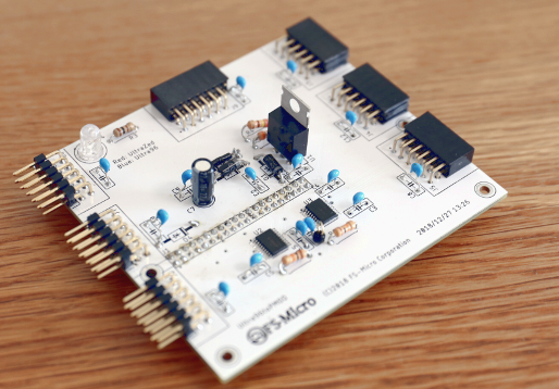
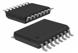
The AD620 Instrumentation Amplifier
AD620 Description
The AD620 is a low cost, high accuracy instrumentation amplifier that the gain can be adjusted up to 10,000 by the incorporation of only a single resistor. Furthermore, the AD620 features 8-lead SOIC and DIP packaging that is smaller than discrete designs and offers lower power (maximum supply current can merely be around 1.3mA), making it a good fit for battery-powered, portable (or remote) applications.
The AD620, with its high accuracy of 40 ppm maximum nonlinearity, low offset voltage of 50 μV max, and offset drift of 0.6 μV/°C max, is ideal for use in precision data acquisition systems, such as weigh scales and transducer interfaces. Furthermore, Low noise and very low value of input bias current render its suitability for medical devices. such as ECG and noninvasive blood pressure monitors.
The low input bias current of 1.0 nA max is made possible with the use of Superϐeta processing in the input stage. The AD620 works well as a preamplifier due to its low input voltage noise of 9 nV/√Hz at 1 kHz, 0.28 μV p-p in the 0.1 Hz to 10 Hz band,
and 0.1 pA/√Hz input current noise. Also, the AD620 is well suited for multiplexed applications with its settling time of 15 μs to 0.01%, and its cost is low enough to enable designs with one in-amp per channel.
AD620 Pinout

AD620 CAD Model
Footprint

AD620 Features
★Easy to use
★Gain set with one external resistor (Gain range 1 to 10,000)
★Wide power supply range (±2.3 V to ±18 V)
★Higher performance than 3 op amp IA designs
★Available in 8-lead DIP and SOIC packaging
★Low power, 1.3 mA max supply current
★Excellent dc performance (B grade)
★Input Offset Voltage: 50 μV
★Input Offset Drift: 0.6 μV/°C
★Input Bias Current: 1.0 nA max
★100 dB min common-mode rejection ratio (G = 10) Low noise
★9 nV/√Hz @ 1 kHz, input voltage noise
★0.28 μV p-p noise (0.1 Hz to 10 Hz)
★Excellent ac specifications
★Bandwidth:120 kHz (G = 100)
★15 μs settling time to 0.01%
Specifications
- TypeParameter
- Contact Plating
Contact plating (finish) provides corrosion protection for base metals and optimizes the mechanical and electrical properties of the contact interfaces.
Lead, Tin - Mount
In electronic components, the term "Mount" typically refers to the method or process of physically attaching or fixing a component onto a circuit board or other electronic device. This can involve soldering, adhesive bonding, or other techniques to secure the component in place. The mounting process is crucial for ensuring proper electrical connections and mechanical stability within the electronic system. Different components may have specific mounting requirements based on their size, shape, and function, and manufacturers provide guidelines for proper mounting procedures to ensure optimal performance and reliability of the electronic device.
Through Hole - Mounting Type
The "Mounting Type" in electronic components refers to the method used to attach or connect a component to a circuit board or other substrate, such as through-hole, surface-mount, or panel mount.
Through Hole - Package / Case
refers to the protective housing that encases an electronic component, providing mechanical support, electrical connections, and thermal management.
8-DIP (0.300, 7.62mm) - Number of Pins8
- Number of Elements1
- Operating Temperature
The operating temperature is the range of ambient temperature within which a power supply, or any other electrical equipment, operate in. This ranges from a minimum operating temperature, to a peak or maximum operating temperature, outside which, the power supply may fail.
-40°C~85°C - Packaging
Semiconductor package is a carrier / shell used to contain and cover one or more semiconductor components or integrated circuits. The material of the shell can be metal, plastic, glass or ceramic.
Tube - JESD-609 Code
The "JESD-609 Code" in electronic components refers to a standardized marking code that indicates the lead-free solder composition and finish of electronic components for compliance with environmental regulations.
e0 - Pbfree Code
The "Pbfree Code" parameter in electronic components refers to the code or marking used to indicate that the component is lead-free. Lead (Pb) is a toxic substance that has been widely used in electronic components for many years, but due to environmental concerns, there has been a shift towards lead-free alternatives. The Pbfree Code helps manufacturers and users easily identify components that do not contain lead, ensuring compliance with regulations and promoting environmentally friendly practices. It is important to pay attention to the Pbfree Code when selecting electronic components to ensure they meet the necessary requirements for lead-free applications.
no - Part Status
Parts can have many statuses as they progress through the configuration, analysis, review, and approval stages.
Obsolete - Moisture Sensitivity Level (MSL)
Moisture Sensitivity Level (MSL) is a standardized rating that indicates the susceptibility of electronic components, particularly semiconductors, to moisture-induced damage during storage and the soldering process, defining the allowable exposure time to ambient conditions before they require special handling or baking to prevent failures
1 (Unlimited) - Number of Terminations8
- ECCN Code
An ECCN (Export Control Classification Number) is an alphanumeric code used by the U.S. Bureau of Industry and Security to identify and categorize electronic components and other dual-use items that may require an export license based on their technical characteristics and potential for military use.
EAR99 - Resistance
Resistance is a fundamental property of electronic components that measures their opposition to the flow of electric current. It is denoted by the symbol "R" and is measured in ohms (Ω). Resistance is caused by the collisions of electrons with atoms in a material, which generates heat and reduces the flow of current. Components with higher resistance will impede the flow of current more than those with lower resistance. Resistance plays a crucial role in determining the behavior and functionality of electronic circuits, such as limiting current flow, voltage division, and controlling power dissipation.
10GOhm - Max Power Dissipation
The maximum power that the MOSFET can dissipate continuously under the specified thermal conditions.
650mW - Terminal Position
In electronic components, the term "Terminal Position" refers to the physical location of the connection points on the component where external electrical connections can be made. These connection points, known as terminals, are typically used to attach wires, leads, or other components to the main body of the electronic component. The terminal position is important for ensuring proper connectivity and functionality of the component within a circuit. It is often specified in technical datasheets or component specifications to help designers and engineers understand how to properly integrate the component into their circuit designs.
DUAL - Number of Functions1
- Supply Voltage
Supply voltage refers to the electrical potential difference provided to an electronic component or circuit. It is crucial for the proper operation of devices, as it powers their functions and determines performance characteristics. The supply voltage must be within specified limits to ensure reliability and prevent damage to components. Different electronic devices have specific supply voltage requirements, which can vary widely depending on their design and intended application.
15V - Terminal Pitch
The center distance from one pole to the next.
2.54mm - Base Part Number
The "Base Part Number" (BPN) in electronic components serves a similar purpose to the "Base Product Number." It refers to the primary identifier for a component that captures the essential characteristics shared by a group of similar components. The BPN provides a fundamental way to reference a family or series of components without specifying all the variations and specific details.
AD620 - Pin Count
a count of all of the component leads (or pins)
8 - Operating Supply Voltage
The voltage level by which an electrical system is designated and to which certain operating characteristics of the system are related.
36V - Operating Supply Current
Operating Supply Current, also known as supply current or quiescent current, is a crucial parameter in electronic components that indicates the amount of current required for the device to operate under normal conditions. It represents the current drawn by the component from the power supply while it is functioning. This parameter is important for determining the power consumption of the component and is typically specified in datasheets to help designers calculate the overall power requirements of their circuits. Understanding the operating supply current is essential for ensuring proper functionality and efficiency of electronic systems.
1.3mA - Nominal Supply Current
Nominal current is the same as the rated current. It is the current drawn by the motor while delivering rated mechanical output at its shaft.
1.3mA - Power Dissipation
the process by which an electronic or electrical device produces heat (energy loss or waste) as an undesirable derivative of its primary action.
650mW - Slew Rate
the maximum rate of output voltage change per unit time.
1.2V/μs - Amplifier Type
Amplifier Type refers to the classification or categorization of amplifiers based on their design, functionality, and characteristics. Amplifiers are electronic devices that increase the amplitude of a signal, such as voltage or current. The type of amplifier determines its specific application, performance capabilities, and operating characteristics. Common types of amplifiers include operational amplifiers (op-amps), power amplifiers, audio amplifiers, and radio frequency (RF) amplifiers. Understanding the amplifier type is crucial for selecting the right component for a particular circuit or system design.
Instrumentation - Common Mode Rejection Ratio
Common Mode Rejection Ratio (CMRR) is a measure of the ability of a differential amplifier to reject input signals that are common to both input terminals. It is defined as the ratio of the differential gain to the common mode gain. A high CMRR indicates that the amplifier can effectively eliminate noise and interference that affects both inputs simultaneously, enhancing the fidelity of the amplified signal. CMRR is typically expressed in decibels (dB), with higher values representing better performance in rejecting common mode signals.
93 dB - Current - Input Bias
The parameter "Current - Input Bias" in electronic components refers to the amount of current required at the input terminal of a device to maintain proper operation. It is a crucial specification as it determines the minimum input current needed for the component to function correctly. Input bias current can affect the performance and accuracy of the device, especially in precision applications where small signal levels are involved. It is typically specified in datasheets for operational amplifiers, transistors, and other semiconductor devices to provide users with important information for circuit design and analysis.
500pA - Voltage - Supply, Single/Dual (±)
The parameter "Voltage - Supply, Single/Dual (±)" in electronic components refers to the power supply voltage required for the proper operation of the component. This parameter indicates whether the component requires a single power supply voltage (e.g., 5V) or a dual power supply voltage (e.g., ±15V). For components that require a single power supply voltage, only one voltage level is needed for operation. On the other hand, components that require a dual power supply voltage need both positive and negative voltage levels to function correctly.Understanding the voltage supply requirements of electronic components is crucial for designing and integrating them into circuits to ensure proper functionality and prevent damage due to incorrect voltage levels.
4.6V~36V ±2.3V~18V - Output Current per Channel
Output Current per Channel is a specification commonly found in electronic components such as amplifiers, audio interfaces, and power supplies. It refers to the maximum amount of electrical current that can be delivered by each individual output channel of the component. This parameter is important because it determines the capacity of the component to drive connected devices or loads. A higher output current per channel means the component can deliver more power to connected devices, while a lower output current may limit the performance or functionality of the component in certain applications. It is crucial to consider the output current per channel when selecting electronic components to ensure they can meet the power requirements of the intended system or setup.
18mA - Input Offset Voltage (Vos)
Input Offset Voltage (Vos) is a key parameter in electronic components, particularly in operational amplifiers. It refers to the voltage difference that must be applied between the two input terminals of the amplifier to nullify the output voltage when the input terminals are shorted together. In simpler terms, it represents the voltage required to bring the output of the amplifier to zero when there is no input signal present. Vos is an important parameter as it can introduce errors in the output signal of the amplifier, especially in precision applications where accuracy is crucial. Minimizing Vos is essential to ensure the amplifier operates with high precision and accuracy.
30mV - Neg Supply Voltage-Nom (Vsup)
The parameter "Neg Supply Voltage-Nom (Vsup)" in electronic components refers to the nominal negative supply voltage that the component requires to operate within its specified performance characteristics. This parameter indicates the minimum voltage level that must be provided to the component's negative supply pin for proper functionality. It is important to ensure that the negative supply voltage provided to the component does not exceed the maximum specified value to prevent damage or malfunction. Understanding and adhering to the specified negative supply voltage requirements is crucial for the reliable operation of the electronic component in a circuit.
-15V - Voltage - Input Offset
Voltage - Input Offset is a parameter that refers to the difference in voltage between the input terminals of an electronic component, such as an operational amplifier, when the input voltage is zero. It is an important characteristic that can affect the accuracy and performance of the component in various applications. A low input offset voltage is desirable as it indicates that the component will have minimal error in its output when the input signal is near zero. Manufacturers typically provide this specification in the component's datasheet to help users understand the component's behavior and make informed decisions when designing circuits.
15μV - -3db Bandwidth
The "-3dB bandwidth" of an electronic component refers to the frequency range over which the component's output signal power is reduced by 3 decibels (dB) compared to its maximum output power. This parameter is commonly used to describe the frequency response of components such as amplifiers, filters, and other signal processing devices. The -3dB point is significant because it represents the half-power point, where the output signal power is reduced to half of its maximum value. Understanding the -3dB bandwidth is important for designing and analyzing electronic circuits to ensure that signals are accurately processed within the desired frequency range.
1MHz - Input Offset Current-Max (IIO)
Input Offset Current-Max (IIO) is a parameter that describes the maximum difference in input bias currents between two input terminals of an electronic component, such as an operational amplifier. Input offset current can cause errors in the output of the component, especially in precision applications where accuracy is crucial. The IIO specification provides a limit on the maximum allowable difference in input currents to ensure that the component operates within its specified performance range. Designers need to consider the IIO value when selecting components and designing circuits to minimize errors and ensure reliable operation.
0.00075μA - Voltage Gain-Min
Voltage Gain-Min is a parameter used to describe the minimum amplification factor of an electronic component, such as an amplifier or transistor. It represents the smallest amount by which the input voltage signal is amplified to produce the output voltage signal. A higher Voltage Gain-Min value indicates a greater amplification capability of the component. This parameter is crucial in determining the performance and efficiency of electronic circuits, as it directly influences the signal strength and quality of the output. Manufacturers provide this specification to help engineers and designers select the appropriate components for their specific application requirements.
1 - Voltage Gain-Nom
Voltage Gain-Nom is a parameter used to describe the ratio of the output voltage to the input voltage in electronic components such as amplifiers. It represents the amplification factor of the component and indicates how much the input voltage is amplified to produce the output voltage. The "Nom" in the term signifies that this value is the nominal or typical voltage gain under specified operating conditions. A higher voltage gain indicates a greater amplification of the input signal, while a lower voltage gain signifies less amplification. This parameter is crucial in determining the performance and functionality of electronic circuits and devices.
10 - Non-linearity-Max
Non-linearity-Max is a parameter used to describe the maximum level of non-linearity exhibited by an electronic component or system. Non-linearity refers to the deviation of the component's output from a straight line when compared to its input signal. In the context of electronic components, such as amplifiers or sensors, non-linearity can introduce distortion or inaccuracies in the output signal. The "Non-linearity-Max" parameter specifies the maximum amount of deviation allowed before the component is considered to be operating outside of its specified linear range. It is an important characteristic to consider when designing or selecting components for applications where precise and accurate signal processing is required.
0.004% - Length9.27mm
- Height Seated (Max)
Height Seated (Max) is a parameter in electronic components that refers to the maximum allowable height of the component when it is properly seated or installed on a circuit board or within an enclosure. This specification is crucial for ensuring proper fit and alignment within the overall system design. Exceeding the maximum seated height can lead to mechanical interference, electrical shorts, or other issues that may impact the performance and reliability of the electronic device. Manufacturers provide this information to help designers and engineers select components that will fit within the designated space and function correctly in the intended application.
4.57mm - Radiation Hardening
Radiation hardening is the process of making electronic components and circuits resistant to damage or malfunction caused by high levels of ionizing radiation, especially for environments in outer space (especially beyond the low Earth orbit), around nuclear reactors and particle accelerators, or during nuclear accidents or nuclear warfare.
No - RoHS Status
RoHS means “Restriction of Certain Hazardous Substances” in the “Hazardous Substances Directive” in electrical and electronic equipment.
Non-RoHS Compliant - Lead Free
Lead Free is a term used to describe electronic components that do not contain lead as part of their composition. Lead is a toxic material that can have harmful effects on human health and the environment, so the electronics industry has been moving towards lead-free components to reduce these risks. Lead-free components are typically made using alternative materials such as silver, copper, and tin. Manufacturers must comply with regulations such as the Restriction of Hazardous Substances (RoHS) directive to ensure that their products are lead-free and environmentally friendly.
Contains Lead
AD620 Alternatives

AD620 Simplified Schematic

Where to use AD620?
The AD620, with its high accuracy of 40 ppm maximum nonlinearity, low offset voltage of 50 μV max, and offset drift of 0.6 μV/°C max, is ideal for use in precision data acquisition systems, such as weigh scales and transducer interfaces. Furthermore, the low noise, low input bias current, and low power of the AD620 make it well suited for medical applications, such as ECG and non-invasive blood pressure monitors.
How to use AD620?
The AD620 only requires a resistor to sets its gain value and hence can be easily set up. A very basic commonly used circuit for AD620 is shown below.

The IC is powered using the pin 7 and pin 4 is connected to ground. Here I have used a singly supply of +5V. The non - inverting pin (pin 2) and the inverting pin (pin 3) is connected the signal which has to be amplified or compared base on the application of the Op-Amp. The Reference pin (pin 5) is normally grounded along with pin 4, the reference pin is used to direct the output towards a voltage when the difference voltage between the inverting and the non-inverting pin is 0V.
The Gain of an Op-Amp can be set by simply connecting the right value of resistor across the pin +Rg (pin 8) and the pin –Rg (pin 1). Here I have connected a resistor of value 500Ω which will set the Op-Amp at a gain value of 100. The formulae to calculate the value of gain from R is given below
G = (49.4 kΏ / RG) + 1
AD620 Applications
★Transducer interface
★Data acquisition systems
★Industrial process controls
★Blood Pressure Monitor
★Medical ECG
★Weigh Scales
★Battery operated and portable Devices
AD620 Package

AD620 Manufacturer
ADI (NASDAQ: ADI) is the world leader in the design, manufacture and marketing of a broad portfolio of high-performance analog, mixed-signal, and digital signal processing (DSP) integrated circuits (IC) electronic devices. Since our establishment in 1965, we have been focusing on solving engineering challenges related to signal processing in electronic equipment. Our signal processing products are used by more than 100,000 customers around the world, and play an important role in converting, regulating and processing real-world phenomena such as temperature, pressure, sound, light, speed and motion into electrical signals for use in a wide array of Electronic equipment.
Trend Analysis
Datasheet PDF
- Datasheets :
- ConflictMineralStatement :
1.Can the amplifier AD623 and AD620 interchangeable?
Both AD620 and AD623 are single instrumentation amplifiers, and the pin arrangement is exactly the same.
The main difference is: AD620 must use positive and negative power supplies, AD623 can be a positive and negative power supply or a single power supply.
If the original board is AD620, you can replace it with 623; if the original board is AD623, you may not be able to replace it with 620 (depending on whether the power supply of the original board circuit is dual power supply or single power supply).
After the replacement of AD620 and AD623 in the single-chip product, the program can work normally without modification.
2.What do the pins of AD620 mean?
P1 and P8 pins are connected to external gain setting resistors.
P2 and P3 pins are input terminals.
P6 pin is the output terminal.
P4 and P7 pins are connected to ±5V power supply
P5 pin is the input reference voltage 400mv
3.What is the working principle of AD620?
AD620 is developed from the traditional three operational amplifiers, but some of the main performance is better than the design of the instrument amplifier composed of three operational amplifiers. For example, the power supply range is wide (±2.3~±18 V), the design volume is small, and the power consumption is very high. Low (the maximum power supply current is only 1. 3 mA), so it is suitable for low-voltage, low-power applications.
The monolithic structure and laser crystal adjustment of AD620 allow circuit components to be closely matched and tracked, thereby ensuring the inherent high performance of the circuit. AD620 is a three-op-amp integrated instrumentation amplifier structure. In order to protect the high precision of gain control, the input transistor provides a simple differential bipolar input, and uses the β process to obtain lower input bias current, through the input stage internal op-amp The feedback of the input transistor keeps the collector current of the input transistor constant, and the input voltage is added to the external gain control resistor RG. The two internal gain resistors of AD620 are 24.7 k8, so the gain equation is G =49.4 kΩ/R G + 1 (1) For the required gain, the external control resistance value is R G =49.4/(G-1)kΩ (2)
4.What signal does AD620 output?
AD620 is an instrumentation amplifier with adjustable voltage gain, and the output is a voltage signal.
5.Why is the input of the AD620 amplifier I connected with positive and negative 5 volts and the output is always negative?
Because it is an instrumentation amplifier structure,
You connect an adjustable resistor to the two pins of the gain amplifier adjustment,
It should be noted that the resistance value should not exceed the value of DATASHEET,
Moreover, do not adjust the magnification too much. If your input line has an uneven interference signal, it will be amplified and output.
(1)The multiple of the first level should not be too high
(2) The bias resistance is not balanced
 AD590KF vs Thermocouples Comparison
23 July 202574
 AT89S52-24PU Microcontroller: Diagram, Pinout, and Datasheet
04 March 20227624
 TXS0108EPWR: Applications, Features and Datasheet
18 October 20231265
 N25Q256A13ESF40G FLASH - NOR Memory IC 256Mb SPI 108 MHz: Datasheet, Features, And Pinout
21 March 20221523
 LM4041 Bandgap Circuit: Pinout, Features and Datasheet
05 November 2021904
 Texas Instruments TMUX1574RSVR: Steps to Solve Common Issues
16 August 2025263
 dsPIC33FJ128GP206: High-Performance Digital Signal Controller Overview
28 February 2024104
 PCA9555 CMOS Device: Datasheet, Pinout, Application Circuit
21 October 20214937
 Discovering Optimal Materials for Wide Bandgap Semiconductors
20 January 20242104
 What is Digital Counter?
01 September 202012309
 Switching Diodes Basics: Working, Types and Circuit Analysis
24 October 202541488
 Parking Access Control System using Arduino
29 August 20235813
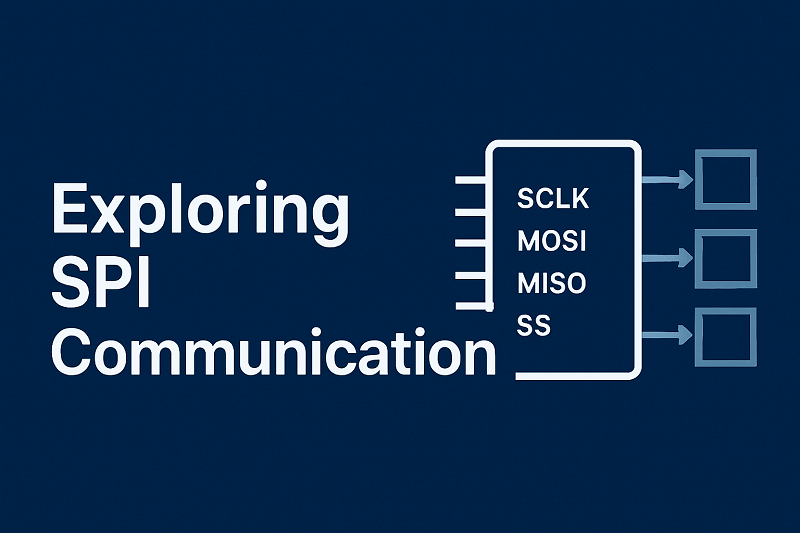 Exploring SPI Communication for Faster Data Transfer
20 June 2025818
 The Through Hole of the PCB Circuit Board Must be Plugged, Why?
14 February 20234670
 Unveiling the Potential of GaN Semiconductor-Enabled Three-Phase Propulsion Inverters for Enhanced EV Performance
09 August 20231558
 Step-by-Step Guide to 2.2 k Ohm Resistor Color Code in 2025
20 August 20252660
Analog Devices Inc.
In Stock: 11400
United States
China
Canada
Japan
Russia
Germany
United Kingdom
Singapore
Italy
Hong Kong(China)
Taiwan(China)
France
Korea
Mexico
Netherlands
Malaysia
Austria
Spain
Switzerland
Poland
Thailand
Vietnam
India
United Arab Emirates
Afghanistan
Åland Islands
Albania
Algeria
American Samoa
Andorra
Angola
Anguilla
Antigua & Barbuda
Argentina
Armenia
Aruba
Australia
Azerbaijan
Bahamas
Bahrain
Bangladesh
Barbados
Belarus
Belgium
Belize
Benin
Bermuda
Bhutan
Bolivia
Bonaire, Sint Eustatius and Saba
Bosnia & Herzegovina
Botswana
Brazil
British Indian Ocean Territory
British Virgin Islands
Brunei
Bulgaria
Burkina Faso
Burundi
Cabo Verde
Cambodia
Cameroon
Cayman Islands
Central African Republic
Chad
Chile
Christmas Island
Cocos (Keeling) Islands
Colombia
Comoros
Congo
Congo (DRC)
Cook Islands
Costa Rica
Côte d’Ivoire
Croatia
Cuba
Curaçao
Cyprus
Czechia
Denmark
Djibouti
Dominica
Dominican Republic
Ecuador
Egypt
El Salvador
Equatorial Guinea
Eritrea
Estonia
Eswatini
Ethiopia
Falkland Islands
Faroe Islands
Fiji
Finland
French Guiana
French Polynesia
Gabon
Gambia
Georgia
Ghana
Gibraltar
Greece
Greenland
Grenada
Guadeloupe
Guam
Guatemala
Guernsey
Guinea
Guinea-Bissau
Guyana
Haiti
Honduras
Hungary
Iceland
Indonesia
Iran
Iraq
Ireland
Isle of Man
Israel
Jamaica
Jersey
Jordan
Kazakhstan
Kenya
Kiribati
Kosovo
Kuwait
Kyrgyzstan
Laos
Latvia
Lebanon
Lesotho
Liberia
Libya
Liechtenstein
Lithuania
Luxembourg
Macao(China)
Madagascar
Malawi
Maldives
Mali
Malta
Marshall Islands
Martinique
Mauritania
Mauritius
Mayotte
Micronesia
Moldova
Monaco
Mongolia
Montenegro
Montserrat
Morocco
Mozambique
Myanmar
Namibia
Nauru
Nepal
New Caledonia
New Zealand
Nicaragua
Niger
Nigeria
Niue
Norfolk Island
North Korea
North Macedonia
Northern Mariana Islands
Norway
Oman
Pakistan
Palau
Palestinian Authority
Panama
Papua New Guinea
Paraguay
Peru
Philippines
Pitcairn Islands
Portugal
Puerto Rico
Qatar
Réunion
Romania
Rwanda
Samoa
San Marino
São Tomé & Príncipe
Saudi Arabia
Senegal
Serbia
Seychelles
Sierra Leone
Sint Maarten
Slovakia
Slovenia
Solomon Islands
Somalia
South Africa
South Sudan
Sri Lanka
St Helena, Ascension, Tristan da Cunha
St. Barthélemy
St. Kitts & Nevis
St. Lucia
St. Martin
St. Pierre & Miquelon
St. Vincent & Grenadines
Sudan
Suriname
Svalbard & Jan Mayen
Sweden
Syria
Tajikistan
Tanzania
Timor-Leste
Togo
Tokelau
Tonga
Trinidad & Tobago
Tunisia
Turkey
Turkmenistan
Turks & Caicos Islands
Tuvalu
U.S. Outlying Islands
U.S. Virgin Islands
Uganda
Ukraine
Uruguay
Uzbekistan
Vanuatu
Vatican City
Venezuela
Wallis & Futuna
Yemen
Zambia
Zimbabwe
![AD826AR-REEL7]() AD826AR-REEL7
AD826AR-REEL7Analog Devices Inc.
![AD8062ARM]() AD8062ARM
AD8062ARMAnalog Devices Inc.
![AD8532ARU-REEL]() AD8532ARU-REEL
AD8532ARU-REELAnalog Devices Inc.
![OP113ES]() OP113ES
OP113ESAnalog Devices Inc.
![SSM2142P]() SSM2142P
SSM2142PAnalog Devices, Inc.
![LTC1050CS8]() LTC1050CS8
LTC1050CS8Linear Technology/Analog Devices
![AMP02EPZ]() AMP02EPZ
AMP02EPZAnalog Devices Inc.
![AD822ARZ-REEL7]() AD822ARZ-REEL7
AD822ARZ-REEL7Analog Devices Inc.
![OP2177ARZ-REEL7]() OP2177ARZ-REEL7
OP2177ARZ-REEL7Analog Devices Inc.
![AD8066ARZ-R7]() AD8066ARZ-R7
AD8066ARZ-R7Analog Devices Inc.


