
 Product
 Brand
Brand Articles
 Tools
Tools
BC557 PNP Transistor: Pinout, Application, and Datasheet


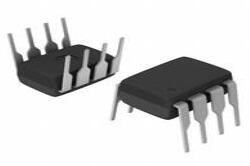
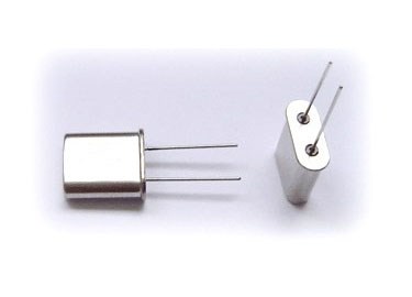
TRANS PNP 45V 0.1A TO-92
BC557 is a widely used PNP bipolar junction transistor manufactured in small TO-92 package.

Top 4 Electronic Project Using BC547 BC557 RGB LED's Capacitor & More Eletronic Components
BC557 Description
The BC557 is a widely used PNP bipolar junction transistor manufactured in small TO-92 package. It is a general purpose PNP transistor that can be used as a switch or amplifier in electronic circuits. Its HFE ratings are 125 to 800, which makes it an ideal transistor to use as a small signal amplifier in electronic circuits such as audio signal amplification.
The max collector dissipation is 500 milliwatt which makes it suitable to use in amplification stages. Moreover it will also perform well when used it as a switch for load under 100mA. The transistor has also good collector to emitter (VCE) value that is -45V, therefore you can easily use it in circuits using 40 to 45 volts DC.
The HFE ratings of BC557 can be determined by the last letter after its number. For example, BC557A HFE ratings are 110-220, BC557B HFE ratings are 200-450 and BC557C HFE ratings are 420-800.
BC557 Pinout


BC557 CAD Model
Symbol

Footprint

3D Model

BC557 Features
Package Type: TO-92
Transistor Type: PNP
Max Collector Current(IC): -100mA
Max Collector-Emitter Voltage (VCE): -45V
Max Collector-Base Voltage (VCB): -50V
Max Emitter-Base Voltage (VBE): -5V
Max Collector Dissipation (Pc): 500 Milliwatt
Max Transition Frequency (fT): 100 MHz
Minimum & Maximum DC Current Gain (hFE): 125 to 800
Max Storage & Operating temperature Should be: -65 to +150Centigrade
Specifications
- TypeParameter
- Lifecycle Status
Lifecycle Status refers to the current stage of an electronic component in its product life cycle, indicating whether it is active, obsolete, or transitioning between these states. An active status means the component is in production and available for purchase. An obsolete status indicates that the component is no longer being manufactured or supported, and manufacturers typically provide a limited time frame for support. Understanding the lifecycle status is crucial for design engineers to ensure continuity and reliability in their projects.
OBSOLETE (Last Updated: 1 week ago) - Mount
In electronic components, the term "Mount" typically refers to the method or process of physically attaching or fixing a component onto a circuit board or other electronic device. This can involve soldering, adhesive bonding, or other techniques to secure the component in place. The mounting process is crucial for ensuring proper electrical connections and mechanical stability within the electronic system. Different components may have specific mounting requirements based on their size, shape, and function, and manufacturers provide guidelines for proper mounting procedures to ensure optimal performance and reliability of the electronic device.
Through Hole - Mounting Type
The "Mounting Type" in electronic components refers to the method used to attach or connect a component to a circuit board or other substrate, such as through-hole, surface-mount, or panel mount.
Through Hole - Package / Case
refers to the protective housing that encases an electronic component, providing mechanical support, electrical connections, and thermal management.
TO-226-3, TO-92-3 (TO-226AA) - Number of Pins3
- Supplier Device Package
The parameter "Supplier Device Package" in electronic components refers to the physical packaging or housing of the component as provided by the supplier. It specifies the form factor, dimensions, and layout of the component, which are crucial for compatibility and integration into electronic circuits and systems. The supplier device package information typically includes details such as the package type (e.g., DIP, SOP, QFN), number of pins, pitch, and overall size, allowing engineers and designers to select the appropriate component for their specific application requirements. Understanding the supplier device package is essential for proper component selection, placement, and soldering during the manufacturing process to ensure optimal performance and reliability of the electronic system.
TO-92-3 - Weight200mg
- Manufacturer Package Identifier
The Manufacturer Package Identifier is a unique code or label assigned by the manufacturer to identify a specific package or housing style of an electronic component. This identifier helps in distinguishing between different package types of the same component, such as integrated circuits, transistors, or diodes. It typically includes information about the package dimensions, lead configuration, and other physical characteristics of the component. The Manufacturer Package Identifier is crucial for ensuring compatibility and proper assembly of electronic components in various devices and circuits.
MKT-2A03DREV4 - Collector-Emitter Breakdown Voltage45V
- Collector-Emitter Saturation Voltage-250mV
- Current-Collector (Ic) (Max)100mA
- Number of Elements1
- hFEMin110
- Operating Temperature
The operating temperature is the range of ambient temperature within which a power supply, or any other electrical equipment, operate in. This ranges from a minimum operating temperature, to a peak or maximum operating temperature, outside which, the power supply may fail.
150°C TJ - Packaging
Semiconductor package is a carrier / shell used to contain and cover one or more semiconductor components or integrated circuits. The material of the shell can be metal, plastic, glass or ceramic.
Bulk - Part Status
Parts can have many statuses as they progress through the configuration, analysis, review, and approval stages.
Obsolete - Moisture Sensitivity Level (MSL)
Moisture Sensitivity Level (MSL) is a standardized rating that indicates the susceptibility of electronic components, particularly semiconductors, to moisture-induced damage during storage and the soldering process, defining the allowable exposure time to ambient conditions before they require special handling or baking to prevent failures
1 (Unlimited) - Termination
Termination in electronic components refers to the practice of matching the impedance of a circuit to prevent signal reflections and ensure maximum power transfer. It involves the use of resistors or other components at the end of transmission lines or connections. Proper termination is crucial in high-frequency applications to maintain signal integrity and reduce noise.
Through Hole - Max Operating Temperature
The Maximum Operating Temperature is the maximum body temperature at which the thermistor is designed to operate for extended periods of time with acceptable stability of its electrical characteristics.
150°C - Min Operating Temperature
The "Min Operating Temperature" parameter in electronic components refers to the lowest temperature at which the component is designed to operate effectively and reliably. This parameter is crucial for ensuring the proper functioning and longevity of the component, as operating below this temperature may lead to performance issues or even damage. Manufacturers specify the minimum operating temperature to provide guidance to users on the environmental conditions in which the component can safely operate. It is important to adhere to this parameter to prevent malfunctions and ensure the overall reliability of the electronic system.
-55°C - Voltage - Rated DC
Voltage - Rated DC is a parameter that specifies the maximum direct current (DC) voltage that an electronic component can safely handle without being damaged. This rating is crucial for ensuring the proper functioning and longevity of the component in a circuit. Exceeding the rated DC voltage can lead to overheating, breakdown, or even permanent damage to the component. It is important to carefully consider this parameter when designing or selecting components for a circuit to prevent any potential issues related to voltage overload.
-45V - Max Power Dissipation
The maximum power that the MOSFET can dissipate continuously under the specified thermal conditions.
500mW - Current Rating
Current rating is the maximum current that a fuse will carry for an indefinite period without too much deterioration of the fuse element.
-100mA - Frequency
In electronic components, the parameter "Frequency" refers to the rate at which a signal oscillates or cycles within a given period of time. It is typically measured in Hertz (Hz) and represents how many times a signal completes a full cycle in one second. Frequency is a crucial aspect in electronic components as it determines the behavior and performance of various devices such as oscillators, filters, and communication systems. Understanding the frequency characteristics of components is essential for designing and analyzing electronic circuits to ensure proper functionality and compatibility with other components in a system.
150MHz - Base Part Number
The "Base Part Number" (BPN) in electronic components serves a similar purpose to the "Base Product Number." It refers to the primary identifier for a component that captures the essential characteristics shared by a group of similar components. The BPN provides a fundamental way to reference a family or series of components without specifying all the variations and specific details.
BC557 - Polarity
In electronic components, polarity refers to the orientation or direction in which the component must be connected in a circuit to function properly. Components such as diodes, capacitors, and LEDs have polarity markings to indicate which terminal should be connected to the positive or negative side of the circuit. Connecting a component with incorrect polarity can lead to malfunction or damage. It is important to pay attention to polarity markings and follow the manufacturer's instructions to ensure proper operation of electronic components.
PNP - Element Configuration
The distribution of electrons of an atom or molecule (or other physical structure) in atomic or molecular orbitals.
Single - Power Dissipation
the process by which an electronic or electrical device produces heat (energy loss or waste) as an undesirable derivative of its primary action.
500mW - Power - Max
Power - Max is a parameter that specifies the maximum amount of power that an electronic component can handle without being damaged. It is typically measured in watts and indicates the upper limit of power that can be safely supplied to the component. Exceeding the maximum power rating can lead to overheating, malfunction, or permanent damage to the component. It is important to consider the power-max rating when designing circuits or systems to ensure proper operation and longevity of the electronic components.
500mW - Gain Bandwidth Product
The gain–bandwidth product (designated as GBWP, GBW, GBP, or GB) for an amplifier is the product of the amplifier's bandwidth and the gain at which the bandwidth is measured.
150MHz - Transistor Type
Transistor type refers to the classification of transistors based on their operation and construction. The two primary types are bipolar junction transistors (BJTs) and field-effect transistors (FETs). BJTs use current to control the flow of current, while FETs utilize voltage to control current flow. Each type has its own subtypes, such as NPN and PNP for BJTs, and MOSFETs and JFETs for FETs, impacting their applications and characteristics in electronic circuits.
PNP - Collector Emitter Voltage (VCEO)
Collector-Emitter Voltage (VCEO) is a key parameter in electronic components, particularly in transistors. It refers to the maximum voltage that can be applied between the collector and emitter terminals of a transistor while the base terminal is open or not conducting. Exceeding this voltage limit can lead to breakdown and potential damage to the transistor. VCEO is crucial for ensuring the safe and reliable operation of the transistor within its specified limits. Designers must carefully consider VCEO when selecting transistors for a circuit to prevent overvoltage conditions that could compromise the performance and longevity of the component.
45V - Max Collector Current
Max Collector Current is a parameter used to specify the maximum amount of current that can safely flow through the collector terminal of a transistor or other electronic component without causing damage. It is typically expressed in units of amperes (A) and is an important consideration when designing circuits to ensure that the component operates within its safe operating limits. Exceeding the specified max collector current can lead to overheating, degradation of performance, or even permanent damage to the component. Designers must carefully consider this parameter when selecting components and designing circuits to ensure reliable and safe operation.
100mA - DC Current Gain (hFE) (Min) @ Ic, Vce
The parameter "DC Current Gain (hFE) (Min) @ Ic, Vce" in electronic components refers to the minimum value of the DC current gain, denoted as hFE, under specific operating conditions of collector current (Ic) and collector-emitter voltage (Vce). The DC current gain hFE represents the ratio of the collector current to the base current in a bipolar junction transistor (BJT), indicating the amplification capability of the transistor. The minimum hFE value at a given Ic and Vce helps determine the transistor's performance and efficiency in amplifying signals within a circuit. Designers use this parameter to ensure proper transistor selection and performance in various electronic applications.
110 @ 2mA 5V - Current - Collector Cutoff (Max)
The parameter "Current - Collector Cutoff (Max)" refers to the maximum current at which a transistor or other electronic component will cease to conduct current between the collector and emitter terminals. This parameter is important in determining the maximum current that can flow through the component when it is in the cutoff state. Exceeding this maximum cutoff current can lead to malfunction or damage of the component. It is typically specified in the component's datasheet and is crucial for proper circuit design and operation.
15nA ICBO - Vce Saturation (Max) @ Ib, Ic
The parameter "Vce Saturation (Max) @ Ib, Ic" in electronic components refers to the maximum voltage drop across the collector-emitter junction when the transistor is in saturation mode. This parameter is specified at a certain base current (Ib) and collector current (Ic) levels. It indicates the minimum voltage required to keep the transistor fully conducting in saturation mode, ensuring that the transistor operates efficiently and does not enter the cutoff region. Designers use this parameter to ensure proper transistor operation and to prevent overheating or damage to the component.
650mV @ 5mA, 100mA - Voltage - Collector Emitter Breakdown (Max)
Voltage - Collector Emitter Breakdown (Max) is a parameter that specifies the maximum voltage that can be applied between the collector and emitter terminals of a transistor or other semiconductor device before it breaks down and allows excessive current to flow. This parameter is crucial for ensuring the safe and reliable operation of the component within its specified limits. Exceeding the maximum breakdown voltage can lead to permanent damage or failure of the device. Designers and engineers must carefully consider this parameter when selecting components for their circuits to prevent potential issues and ensure proper functionality.
45V - Max Frequency
Max Frequency refers to the highest frequency at which an electronic component can operate effectively without degradation of performance. It is a critical parameter for devices such as transistors, capacitors, and oscillators, indicating their limitations in speed and response time. Exceeding the max frequency can lead to issues like signal distortion, heat generation, and potential failure of the component. Understanding this parameter is essential for designing circuits to ensure reliable and efficient operation.
150MHz - Frequency - Transition
The parameter "Frequency - Transition" in electronic components refers to the maximum frequency at which a signal transition can occur within the component. It is a crucial specification for digital circuits as it determines the speed at which data can be processed and transmitted. A higher frequency transition allows for faster operation and better performance of the electronic component. It is typically measured in hertz (Hz) or megahertz (MHz) and is specified by the manufacturer to ensure proper functioning of the component within a given frequency range.
150MHz - Collector Base Voltage (VCBO)
Collector Base Voltage (VCBO) is the maximum allowable voltage that can be applied between the collector and base terminals of a bipolar junction transistor when the emitter is open. It is a critical parameter that determines the voltage rating of the transistor and helps prevent breakdown in the collector-base junction. Exceeding this voltage can lead to permanent damage or failure of the component.
-50V - Emitter Base Voltage (VEBO)
Emitter Base Voltage (VEBO) is a parameter used in electronic components, particularly in transistors. It refers to the maximum voltage that can be applied between the emitter and base terminals of a transistor without causing damage to the device. Exceeding this voltage limit can lead to breakdown of the transistor and potential failure. VEBO is an important specification to consider when designing circuits to ensure the proper operation and reliability of the components. It is typically provided in the datasheet of the transistor and should be carefully observed to prevent any potential damage during operation.
-5V - Height5.33mm
- Length5.2mm
- Width4.19mm
- REACH SVHC
The parameter "REACH SVHC" in electronic components refers to the compliance with the Registration, Evaluation, Authorization, and Restriction of Chemicals (REACH) regulation regarding Substances of Very High Concern (SVHC). SVHCs are substances that may have serious effects on human health or the environment, and their use is regulated under REACH to ensure their safe handling and minimize their impact.Manufacturers of electronic components need to declare if their products contain any SVHCs above a certain threshold concentration and provide information on the safe use of these substances. This information allows customers to make informed decisions about the potential risks associated with using the components and take appropriate measures to mitigate any hazards.Ensuring compliance with REACH SVHC requirements is essential for electronics manufacturers to meet regulatory standards, protect human health and the environment, and maintain transparency in their supply chain. It also demonstrates a commitment to sustainability and responsible manufacturing practices in the electronics industry.
No SVHC - Radiation Hardening
Radiation hardening is the process of making electronic components and circuits resistant to damage or malfunction caused by high levels of ionizing radiation, especially for environments in outer space (especially beyond the low Earth orbit), around nuclear reactors and particle accelerators, or during nuclear accidents or nuclear warfare.
No - RoHS Status
RoHS means “Restriction of Certain Hazardous Substances” in the “Hazardous Substances Directive” in electrical and electronic equipment.
RoHS Compliant - Lead Free
Lead Free is a term used to describe electronic components that do not contain lead as part of their composition. Lead is a toxic material that can have harmful effects on human health and the environment, so the electronics industry has been moving towards lead-free components to reduce these risks. Lead-free components are typically made using alternative materials such as silver, copper, and tin. Manufacturers must comply with regulations such as the Restriction of Hazardous Substances (RoHS) directive to ensure that their products are lead-free and environmentally friendly.
Lead Free
BC557 Functional Alternatives

BC557 NPN Complementary
Where to use BC557
The BC557 is a general purpose transistor that can be used in a wide variety of general purpose applications. It can be used as an audio amplifier in small radios, electronic buzzers, electronic bells and other sound circuits that require small amplification. Due to the good gain of the BC557, it can also be used in audio preamplifier stages. Furthermore, the BC557 can perform as a switch in electronic applications for 100mA load, it can be used to switch any part of an electronic circuit, other high-power transistors, LEDs, relays etc.
How to use BC557
BC557 is a PNP transistor hence the collector and emitter will be closed (Forward biased) when the base pin is held at ground and will be opened (Reverse biased) when a signal is provided to base pin. This is where a PNP transistor differs from a NPN transistor, a Logic state (blue colour) is used to toggle between Ground and Signal Voltage (Emitter-Base Voltage VBE) as shown below

BC557 has a gain value of 110 to 800, this value determines the amplification capacity of the transistor. The maximum amount of current that could flow through the Collector pin is 100mA, hence we cannot connect loads that consume more than 100mA using this transistor. To bias a transistor we have to supply current to base pin, this current (IB) should be limited to 5mA.
When this transistor is fully biased then it can allow a maximum of 100mA to flow across the collector and emitter. This stage is called Saturation Region and the typical voltage allowed across the Collector-Emitter (VCE) or Base-Emitter (VBE) could be 200 and 900 mV respectively. When base current is removed the transistor becomes fully off, this stage is called as the Cut-off Region and the Base Emitter voltage could be around 660 mV.
BC557 as switch
When a transistor is used as a switch it is operated in the Saturation and Cut-Off Region as explained above. As discussed a transistor will act as an Open switch during Forward Bias and as a Closed switch during Reverse Bias, this biasing can be achieved by supplying the required amount of current to the base pin. As mentioned the biasing current should maximum of 5mA. Anything more than 5mA will kill the Transistor; hence a resistor is always added in series with base pin. The value of this resistor (RB) can be calculated using below formulae.
RB = VBE / IB
Where, the value of VBE should be 5V for BC557 and the Base current (IB depends on the Collector current (IC). The value of IB should not exceed mA.
BC557 as Amplifier
A Transistors acts as an Amplifier when operating in Active Region. It can amplify power, voltage and current at different configurations.
Some of the configurations used in amplifier circuits are
Common emitter amplifier
Common collector amplifier
Common base amplifier
Of the above types common emitter type is the popular and mostly used configuration. When uses as an Amplifier the DC current gain of the Transistor can be calculated by using the below formulae
DC Current Gain = Collector Current (IC) / Base Current (IB)
BC557 Applications
Preamplifier
Small signal audio amplifier
Driving Loads under 0.1mA or 100mA
Relay Driver and LED driver
Darlington pair
Robotics and instrumentation projects
Used in motors for controlling current
Low noise input stages of tape recorders
HI-FI amplifiers
Signal processing circuits of television receivers
BC557 Package

BC557 Package Outline
BC557 Manufacturer
ON Semiconductor (Nasdaq: ON) is driving energy efficient innovations, empowering customers to reduce global energy use. The company offers a comprehensive portfolio of energy efficient power and signal management, logic, discrete and custom solutions to help design engineers solve their unique design challenges in automotive, communications, computing, consumer, industrial, LED lighting, medical, military/aerospace and power supply applications. ON Semiconductor operates a responsive, reliable, world-class supply chain and quality program, and a network of manufacturing facilities, sales offices and design centers in key markets throughout North America, Europe, and the Asia Pacific regions.
Trend Analysis
Datasheet PDF
- Datasheets :
- ReachStatement :
1.What is BC557?
BC557 is a PNP transistor hence the collector and emitter will be closed (Forward biased) when the base pin is held at ground and will be opened (Reverse biased) when a signal is provided to base pin.
2.How does BC557 work?
BC557 is a bipolar junction transistor with DC current gain 300. It falls under the category of PNP transistors where one N-doped layer stands between the two P-doped layers. The continuous collector current is 100mA means it can drive load under 100mA.
3.Can I use BC557 instead of BC558?
The equivalent or alternative transistor of both may have a different option, but first, we can say BC557 and BC558 are alternatives to each other. It can be used for any type of general-purpose application.
4.How to safely long run BC557 in a circuit?
To safely run this transistor for good performance for a long time in your electronic circuit it is essential to not operate transistor under -45V DC, always use suitable base resistor, do not provide this transistor more than -100mA load, the operating and storage temperature around the transistor should be under -65 to +150 Centigrade, and always check the pinout of the transistor before placing it in an electronic circuit if wrongly placed then check the transistor again before placing it in the circuit.
5.Can I use BC557 instead of BC547?
The BC547-9 series and BC557-9 series are functionally identical to the common BC107-9 series. All have a maximum power dissipation of 500mW. They have essentially similar specifications and can generally be substituted for one another (within the PNP and NPN groups of three each).
 AD581: High-Precision Voltage Reference for Reliable Electronic Systems
06 March 2024236
![The Overview of ULN2804A [FAQ]](https://res.utmel.com/Images/Article/3181ac35-5dea-4941-9ec1-92b35f724019.jpg) The Overview of ULN2804A [FAQ]
The Overview of ULN2804A [FAQ]18 December 20213721
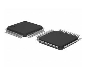 STM32F401RET6TR Microcontroller: 32-Bit, 64-LQFP, Pinout and Features
21 January 20221973
 PL602-21TI-R Clock Generator: Pinout, Equivalent and Datasheet
12 March 2022438
 AT24C256 Two-wire Serial EEPROM: Pinout, Datasheet and Address
06 November 20216766
 A Comprehensive Guide to LTC7138MPMSE#TRPBF DC-DC Switching Regulator
06 March 2024301
 AD708 Dual Precision Op Amp: DC Performance Analysis and Modern Replacement Notes
20 May 2026183
 W25Q128JVSIQ 8SOIC 3V 128M-bit serial flash memory:Datasheet, Pinout ang Package
10 January 20229771
 Analysis of Magnetic and Thermal Semiconductor Power Modules
13 March 20242100
 An overview of Flip-flop
10 December 20204498
 Basic Introduction to Memristor
12 January 202112483
 Introduction to Wearable Sensors
27 October 20252813
 What are Resonators?
07 January 202617664
 Basic Understanding of Attenuators
15 September 202017498
 Huawei's Sensor Layout
24 March 20222807
 Challenges in Enhancing Power Electronic Systems with Artificial Intelligence
26 December 20233138
ON Semiconductor
In Stock: 5000
United States
China
Canada
Japan
Russia
Germany
United Kingdom
Singapore
Italy
Hong Kong(China)
Taiwan(China)
France
Korea
Mexico
Netherlands
Malaysia
Austria
Spain
Switzerland
Poland
Thailand
Vietnam
India
United Arab Emirates
Afghanistan
Åland Islands
Albania
Algeria
American Samoa
Andorra
Angola
Anguilla
Antigua & Barbuda
Argentina
Armenia
Aruba
Australia
Azerbaijan
Bahamas
Bahrain
Bangladesh
Barbados
Belarus
Belgium
Belize
Benin
Bermuda
Bhutan
Bolivia
Bonaire, Sint Eustatius and Saba
Bosnia & Herzegovina
Botswana
Brazil
British Indian Ocean Territory
British Virgin Islands
Brunei
Bulgaria
Burkina Faso
Burundi
Cabo Verde
Cambodia
Cameroon
Cayman Islands
Central African Republic
Chad
Chile
Christmas Island
Cocos (Keeling) Islands
Colombia
Comoros
Congo
Congo (DRC)
Cook Islands
Costa Rica
Côte d’Ivoire
Croatia
Cuba
Curaçao
Cyprus
Czechia
Denmark
Djibouti
Dominica
Dominican Republic
Ecuador
Egypt
El Salvador
Equatorial Guinea
Eritrea
Estonia
Eswatini
Ethiopia
Falkland Islands
Faroe Islands
Fiji
Finland
French Guiana
French Polynesia
Gabon
Gambia
Georgia
Ghana
Gibraltar
Greece
Greenland
Grenada
Guadeloupe
Guam
Guatemala
Guernsey
Guinea
Guinea-Bissau
Guyana
Haiti
Honduras
Hungary
Iceland
Indonesia
Iran
Iraq
Ireland
Isle of Man
Israel
Jamaica
Jersey
Jordan
Kazakhstan
Kenya
Kiribati
Kosovo
Kuwait
Kyrgyzstan
Laos
Latvia
Lebanon
Lesotho
Liberia
Libya
Liechtenstein
Lithuania
Luxembourg
Macao(China)
Madagascar
Malawi
Maldives
Mali
Malta
Marshall Islands
Martinique
Mauritania
Mauritius
Mayotte
Micronesia
Moldova
Monaco
Mongolia
Montenegro
Montserrat
Morocco
Mozambique
Myanmar
Namibia
Nauru
Nepal
New Caledonia
New Zealand
Nicaragua
Niger
Nigeria
Niue
Norfolk Island
North Korea
North Macedonia
Northern Mariana Islands
Norway
Oman
Pakistan
Palau
Palestinian Authority
Panama
Papua New Guinea
Paraguay
Peru
Philippines
Pitcairn Islands
Portugal
Puerto Rico
Qatar
Réunion
Romania
Rwanda
Samoa
San Marino
São Tomé & Príncipe
Saudi Arabia
Senegal
Serbia
Seychelles
Sierra Leone
Sint Maarten
Slovakia
Slovenia
Solomon Islands
Somalia
South Africa
South Sudan
Sri Lanka
St Helena, Ascension, Tristan da Cunha
St. Barthélemy
St. Kitts & Nevis
St. Lucia
St. Martin
St. Pierre & Miquelon
St. Vincent & Grenadines
Sudan
Suriname
Svalbard & Jan Mayen
Sweden
Syria
Tajikistan
Tanzania
Timor-Leste
Togo
Tokelau
Tonga
Trinidad & Tobago
Tunisia
Turkey
Turkmenistan
Turks & Caicos Islands
Tuvalu
U.S. Outlying Islands
U.S. Virgin Islands
Uganda
Ukraine
Uruguay
Uzbekistan
Vanuatu
Vatican City
Venezuela
Wallis & Futuna
Yemen
Zambia
Zimbabwe
![MMBT2222ALT1G]() MMBT2222ALT1G
MMBT2222ALT1GON Semiconductor
![MPSA43]() MPSA43
MPSA43ON Semiconductor
![MMBT3906LT1G]() MMBT3906LT1G
MMBT3906LT1GON Semiconductor
![MMBT5551LT1G]() MMBT5551LT1G
MMBT5551LT1GON Semiconductor
![MMBT4403LT1G]() MMBT4403LT1G
MMBT4403LT1GON Semiconductor
![BC846BLT1G]() BC846BLT1G
BC846BLT1GON Semiconductor
![MMBT3904TT1G]() MMBT3904TT1G
MMBT3904TT1GON Semiconductor
![MMBTA92LT1G]() MMBTA92LT1G
MMBTA92LT1GON Semiconductor
![SMMBT5551LT1G]() SMMBT5551LT1G
SMMBT5551LT1GON Semiconductor
![BCP56-16T1G]() BCP56-16T1G
BCP56-16T1GON Semiconductor


