
 Product
 Brand
Brand Articles
 Tools
Tools
BSS84 Transistor: Features, Pinout, and Datasheet

P-Channel Tape & Reel (TR) 10 Ω @ 100mA, 5V ±20V 45pF @ 25V 50V TO-236-3, SC-59, SOT-23-3


P-Channel Tape & Reel (TR) 10 Ω @ 100mA, 5V ±20V 45pF @ 25V 50V TO-236-3, SC-59, SOT-23-3
The BSS84 can be used with a minimum of effort, in most applications requiring up to 0.13 A DC and can deliver current up to 0.52 A. This article mainly introduces features, pinout, datasheet and other detailed information about Diodes Incorporated BSS84.

KiCad tutorial 7 : Simulation of current source circuit using a power MOSFET BSS84
BSS84 Description
The BSS84 can be used, with a minimum of effort, in most applications requiring up to 0.13 A DC and can deliver current up to 0.52 A. This product is particularly suited to low-voltage applications requiring a low-current high-side switch.
This MOSFET has been designed to minimize the on-state resistance (RDS(ON)) and yet maintain superior switching performance, making it ideal for high-efficiency power management applications.
This P-channel enhancement-mode field-effect transistor is produced using ON Semiconductor’s proprietary, high cell density, DMOS technology. This very high-density process minimizes on-state resistance and provides rugged and reliable performance and fast switching.
BSS84 Pinout

Pinout
BSS84 CAD Model

Symbol

Footprint

3D Model
BSS84 Features
● Low On-Resistance
● Low Gate Threshold Voltage
● Low Input Capacitance
● Fast Switching Speed
● Low Input/Output Leakage
● Totally Lead-Free & Fully RoHS Compliant
● Halogen And Antimony Free. “Green” Device
● The BSS84Q Is Suitable For Automotive Applications Requiring Specific Change Control; This Part Is AEC-Q101 Qualified, PPAP Capable, And Manufactured In IATF 16949 Certified Facilities.
● -0.13 A, -50 V, RDS(ON) = 10 Ω At VGS = -5 V §
● Voltage-Controlled P-Channel Small-Signal Switch §
● High-Density Cell Design For Low RDS(ON) §
● High Saturation Current
Specifications
- TypeParameter
- Factory Lead Time14 Weeks
- Contact Plating
Contact plating (finish) provides corrosion protection for base metals and optimizes the mechanical and electrical properties of the contact interfaces.
Tin - Mount
In electronic components, the term "Mount" typically refers to the method or process of physically attaching or fixing a component onto a circuit board or other electronic device. This can involve soldering, adhesive bonding, or other techniques to secure the component in place. The mounting process is crucial for ensuring proper electrical connections and mechanical stability within the electronic system. Different components may have specific mounting requirements based on their size, shape, and function, and manufacturers provide guidelines for proper mounting procedures to ensure optimal performance and reliability of the electronic device.
Surface Mount - Mounting Type
The "Mounting Type" in electronic components refers to the method used to attach or connect a component to a circuit board or other substrate, such as through-hole, surface-mount, or panel mount.
Surface Mount - Package / Case
refers to the protective housing that encases an electronic component, providing mechanical support, electrical connections, and thermal management.
TO-236-3, SC-59, SOT-23-3 - Number of Pins3
- Weight7.994566mg
- Transistor Element Material
The "Transistor Element Material" parameter in electronic components refers to the material used to construct the transistor within the component. Transistors are semiconductor devices that amplify or switch electronic signals and are a fundamental building block in electronic circuits. The material used for the transistor element can significantly impact the performance and characteristics of the component. Common materials used for transistor elements include silicon, germanium, and gallium arsenide, each with its own unique properties and suitability for different applications. The choice of transistor element material is crucial in designing electronic components to meet specific performance requirements such as speed, power efficiency, and temperature tolerance.
SILICON - Manufacturer Package Identifier
The Manufacturer Package Identifier is a unique code or label assigned by the manufacturer to identify a specific package or housing style of an electronic component. This identifier helps in distinguishing between different package types of the same component, such as integrated circuits, transistors, or diodes. It typically includes information about the package dimensions, lead configuration, and other physical characteristics of the component. The Manufacturer Package Identifier is crucial for ensuring compatibility and proper assembly of electronic components in various devices and circuits.
BSS84-7-F - Current - Continuous Drain (Id) @ 25℃130mA Ta
- Drive Voltage (Max Rds On, Min Rds On)5V
- Number of Elements1
- Power Dissipation (Max)300mW Ta
- Turn Off Delay Time
It is the time from when Vgs drops below 90% of the gate drive voltage to when the drain current drops below 90% of the load current. It is the delay before current starts to transition in the load, and depends on Rg. Ciss.
18 ns - Operating Temperature
The operating temperature is the range of ambient temperature within which a power supply, or any other electrical equipment, operate in. This ranges from a minimum operating temperature, to a peak or maximum operating temperature, outside which, the power supply may fail.
-55°C~150°C TJ - Packaging
Semiconductor package is a carrier / shell used to contain and cover one or more semiconductor components or integrated circuits. The material of the shell can be metal, plastic, glass or ceramic.
Tape & Reel (TR) - Published2008
- JESD-609 Code
The "JESD-609 Code" in electronic components refers to a standardized marking code that indicates the lead-free solder composition and finish of electronic components for compliance with environmental regulations.
e3 - Pbfree Code
The "Pbfree Code" parameter in electronic components refers to the code or marking used to indicate that the component is lead-free. Lead (Pb) is a toxic substance that has been widely used in electronic components for many years, but due to environmental concerns, there has been a shift towards lead-free alternatives. The Pbfree Code helps manufacturers and users easily identify components that do not contain lead, ensuring compliance with regulations and promoting environmentally friendly practices. It is important to pay attention to the Pbfree Code when selecting electronic components to ensure they meet the necessary requirements for lead-free applications.
yes - Part Status
Parts can have many statuses as they progress through the configuration, analysis, review, and approval stages.
Active - Moisture Sensitivity Level (MSL)
Moisture Sensitivity Level (MSL) is a standardized rating that indicates the susceptibility of electronic components, particularly semiconductors, to moisture-induced damage during storage and the soldering process, defining the allowable exposure time to ambient conditions before they require special handling or baking to prevent failures
1 (Unlimited) - Number of Terminations3
- ECCN Code
An ECCN (Export Control Classification Number) is an alphanumeric code used by the U.S. Bureau of Industry and Security to identify and categorize electronic components and other dual-use items that may require an export license based on their technical characteristics and potential for military use.
EAR99 - Resistance
Resistance is a fundamental property of electronic components that measures their opposition to the flow of electric current. It is denoted by the symbol "R" and is measured in ohms (Ω). Resistance is caused by the collisions of electrons with atoms in a material, which generates heat and reduces the flow of current. Components with higher resistance will impede the flow of current more than those with lower resistance. Resistance plays a crucial role in determining the behavior and functionality of electronic circuits, such as limiting current flow, voltage division, and controlling power dissipation.
10Ohm - Additional Feature
Any Feature, including a modified Existing Feature, that is not an Existing Feature.
HIGH RELIABILITY, LOW THRESHOLD - Voltage - Rated DC
Voltage - Rated DC is a parameter that specifies the maximum direct current (DC) voltage that an electronic component can safely handle without being damaged. This rating is crucial for ensuring the proper functioning and longevity of the component in a circuit. Exceeding the rated DC voltage can lead to overheating, breakdown, or even permanent damage to the component. It is important to carefully consider this parameter when designing or selecting components for a circuit to prevent any potential issues related to voltage overload.
-50V - Terminal Position
In electronic components, the term "Terminal Position" refers to the physical location of the connection points on the component where external electrical connections can be made. These connection points, known as terminals, are typically used to attach wires, leads, or other components to the main body of the electronic component. The terminal position is important for ensuring proper connectivity and functionality of the component within a circuit. It is often specified in technical datasheets or component specifications to help designers and engineers understand how to properly integrate the component into their circuit designs.
DUAL - Terminal Form
Occurring at or forming the end of a series, succession, or the like; closing; concluding.
GULL WING - Peak Reflow Temperature (Cel)
Peak Reflow Temperature (Cel) is a parameter that specifies the maximum temperature at which an electronic component can be exposed during the reflow soldering process. Reflow soldering is a common method used to attach electronic components to a circuit board. The Peak Reflow Temperature is crucial because it ensures that the component is not damaged or degraded during the soldering process. Exceeding the specified Peak Reflow Temperature can lead to issues such as component failure, reduced performance, or even permanent damage to the component. It is important for manufacturers and assemblers to adhere to the recommended Peak Reflow Temperature to ensure the reliability and functionality of the electronic components.
260 - Current Rating
Current rating is the maximum current that a fuse will carry for an indefinite period without too much deterioration of the fuse element.
-130mA - Time@Peak Reflow Temperature-Max (s)
Time@Peak Reflow Temperature-Max (s) refers to the maximum duration that an electronic component can be exposed to the peak reflow temperature during the soldering process, which is crucial for ensuring reliable solder joint formation without damaging the component.
40 - Pin Count
a count of all of the component leads (or pins)
3 - Qualification Status
An indicator of formal certification of qualifications.
Not Qualified - Number of Channels1
- Element Configuration
The distribution of electrons of an atom or molecule (or other physical structure) in atomic or molecular orbitals.
Single - Operating Mode
A phase of operation during the operation and maintenance stages of the life cycle of a facility.
ENHANCEMENT MODE - Power Dissipation
the process by which an electronic or electrical device produces heat (energy loss or waste) as an undesirable derivative of its primary action.
300mW - Turn On Delay Time
Turn-on delay, td(on), is the time taken to charge the input capacitance of the device before drain current conduction can start.
10 ns - FET Type
"FET Type" refers to the type of Field-Effect Transistor (FET) being used in an electronic component. FETs are three-terminal semiconductor devices that can be classified into different types based on their construction and operation. The main types of FETs include Metal-Oxide-Semiconductor FETs (MOSFETs), Junction FETs (JFETs), and Insulated-Gate Bipolar Transistors (IGBTs).Each type of FET has its own unique characteristics and applications. MOSFETs are commonly used in digital circuits due to their high input impedance and low power consumption. JFETs are often used in low-noise amplifiers and switching circuits. IGBTs combine the high input impedance of MOSFETs with the high current-carrying capability of bipolar transistors, making them suitable for high-power applications like motor control and power inverters.When selecting an electronic component, understanding the FET type is crucial as it determines the device's performance and suitability for a specific application. It is important to consider factors such as voltage ratings, current handling capabilities, switching speeds, and power dissipation when choosing the right FET type for a particular circuit design.
P-Channel - Transistor Application
In the context of electronic components, the parameter "Transistor Application" refers to the specific purpose or function for which a transistor is designed and used. Transistors are semiconductor devices that can amplify or switch electronic signals and are commonly used in various electronic circuits. The application of a transistor can vary widely depending on its design and characteristics, such as whether it is intended for audio amplification, digital logic, power control, or radio frequency applications. Understanding the transistor application is important for selecting the right type of transistor for a particular circuit or system to ensure optimal performance and functionality.
SWITCHING - Rds On (Max) @ Id, Vgs
Rds On (Max) @ Id, Vgs refers to the maximum on-resistance of a MOSFET or similar transistor when it is fully turned on or in the saturation region. It is specified at a given drain current (Id) and gate-source voltage (Vgs). This parameter indicates how much resistance the component will offer when conducting, impacting power loss and efficiency in a circuit. Lower Rds On values are preferred for better performance in switching applications.
10 Ω @ 100mA, 5V - Vgs(th) (Max) @ Id
The parameter "Vgs(th) (Max) @ Id" in electronic components refers to the maximum gate-source threshold voltage at a specified drain current (Id). This parameter is commonly found in field-effect transistors (FETs) and is used to define the minimum voltage required at the gate terminal to turn on the transistor and allow current to flow from the drain to the source. The maximum value indicates the upper limit of this threshold voltage under specified operating conditions. It is an important parameter for determining the proper biasing and operating conditions of the FET in a circuit to ensure proper functionality and performance.
2V @ 1mA - Input Capacitance (Ciss) (Max) @ Vds
The parameter "Input Capacitance (Ciss) (Max) @ Vds" in electronic components refers to the maximum input capacitance measured at a specific drain-source voltage (Vds). Input capacitance is a crucial parameter in field-effect transistors (FETs) and power MOSFETs, as it represents the total capacitance at the input terminal of the device. This capacitance affects the device's switching speed and overall performance, as it influences the time required for charging and discharging during operation. Manufacturers provide this parameter to help designers understand the device's input characteristics and make informed decisions when integrating it into a circuit.
45pF @ 25V - Drain to Source Voltage (Vdss)
The Drain to Source Voltage (Vdss) is a key parameter in electronic components, particularly in field-effect transistors (FETs) such as MOSFETs. It refers to the maximum voltage that can be applied between the drain and source terminals of the FET without causing damage to the component. Exceeding this voltage limit can lead to breakdown and potentially permanent damage to the device.Vdss is an important specification to consider when designing or selecting components for a circuit, as it determines the operating range and reliability of the FET. It is crucial to ensure that the Vdss rating of the component is higher than the maximum voltage expected in the circuit to prevent failures and ensure proper functionality.In summary, the Drain to Source Voltage (Vdss) is a critical parameter that defines the maximum voltage tolerance of a FET component and plays a significant role in determining the overall performance and reliability of electronic circuits.
50V - Vgs (Max)
Vgs (Max) refers to the maximum gate-source voltage that can be applied to a field-effect transistor (FET) without causing damage to the component. This parameter is crucial in determining the safe operating limits of the FET and helps prevent overvoltage conditions that could lead to device failure. Exceeding the specified Vgs (Max) rating can result in breakdown of the gate oxide layer, leading to permanent damage to the FET. Designers must ensure that the applied gate-source voltage does not exceed the maximum rating to ensure reliable and long-term operation of the electronic component.
±20V - Continuous Drain Current (ID)
Continuous Drain Current (ID) is a key parameter in electronic components, particularly in field-effect transistors (FETs) such as MOSFETs. It refers to the maximum current that can flow continuously through the drain terminal of the FET without causing damage to the component. This parameter is crucial for determining the power handling capability of the FET and is specified by the manufacturer in the component's datasheet. Designers must ensure that the actual operating current does not exceed the specified Continuous Drain Current to prevent overheating and potential failure of the component.
130mA - Threshold Voltage
The threshold voltage is a critical parameter in electronic components, particularly in field-effect transistors (FETs). It refers to the minimum voltage required at the input terminal of the FET to turn it on and allow current to flow between the source and drain terminals. Below the threshold voltage, the FET remains in the off state, acting as an open switch. Once the threshold voltage is exceeded, the FET enters the on state, conducting current between the source and drain.The threshold voltage is a key factor in determining the operating characteristics of FETs, such as their switching speed and power consumption. It is typically specified by the manufacturer and can vary depending on the specific type of FET and its design. Designers must consider the threshold voltage when selecting FETs for a particular application to ensure proper functionality and performance.
-800mV - Gate to Source Voltage (Vgs)
The Gate to Source Voltage (Vgs) is a crucial parameter in electronic components, particularly in field-effect transistors (FETs) such as MOSFETs. It refers to the voltage difference between the gate and source terminals of the FET. This voltage determines the conductivity of the FET and controls the flow of current through the device. By varying the Vgs, the FET can be switched on or off, allowing for precise control of electronic circuits. Understanding and properly managing the Vgs is essential for ensuring the reliable and efficient operation of FET-based circuits.
20V - Height1mm
- Length2.9mm
- Width1.3mm
- REACH SVHC
The parameter "REACH SVHC" in electronic components refers to the compliance with the Registration, Evaluation, Authorization, and Restriction of Chemicals (REACH) regulation regarding Substances of Very High Concern (SVHC). SVHCs are substances that may have serious effects on human health or the environment, and their use is regulated under REACH to ensure their safe handling and minimize their impact.Manufacturers of electronic components need to declare if their products contain any SVHCs above a certain threshold concentration and provide information on the safe use of these substances. This information allows customers to make informed decisions about the potential risks associated with using the components and take appropriate measures to mitigate any hazards.Ensuring compliance with REACH SVHC requirements is essential for electronics manufacturers to meet regulatory standards, protect human health and the environment, and maintain transparency in their supply chain. It also demonstrates a commitment to sustainability and responsible manufacturing practices in the electronics industry.
No SVHC - RoHS Status
RoHS means “Restriction of Certain Hazardous Substances” in the “Hazardous Substances Directive” in electrical and electronic equipment.
ROHS3 Compliant - Lead Free
Lead Free is a term used to describe electronic components that do not contain lead as part of their composition. Lead is a toxic material that can have harmful effects on human health and the environment, so the electronics industry has been moving towards lead-free components to reduce these risks. Lead-free components are typically made using alternative materials such as silver, copper, and tin. Manufacturers must comply with regulations such as the Restriction of Hazardous Substances (RoHS) directive to ensure that their products are lead-free and environmentally friendly.
Lead Free
BSS84 Functional Block Diagram

Functional Block Diagram
BSS84 Layout

Layout
BSS84 Alternatives
| Part Number | Description | Manufacturer |
| BSS84LT1TRANSISTORS | TRANSISTOR,MOSFET,P-CHANNEL,50V V(BR)DSS,100MA I(D),TO-236AB | Freescale Semiconductor |
| BSS84,215TRANSISTORS | BSS84 - P-channel vertical D-MOS logic level FET@en-us TO-236 3-Pin | Nexperia |
| BSS84/DGTRANSISTORS | Small Signal Field-Effect Transistor | Nexperia |
| BSS84LT3TRANSISTORS | Small Signal Field-Effect Transistor, 0.1A I(D), 50V, 1-Element, P-Channel, Silicon, Metal-oxide Semiconductor FET, TO-236AB, CASE 318-08, 3 PIN | Motorola Semiconductor Products |
| BSS84TATRANSISTORS | Small Signal Field-Effect Transistor, 0.13A I(D), 50V, 1-Element, P-Channel, Silicon, Metal-oxide Semiconductor FET, SOT-23, 3 PIN | Zetex / Diodes Inc |
| BSS84-TAPE-7TRANSISTORS | TRANSISTOR 130 mA, 50 V, P-CHANNEL, Si, SMALL SIGNAL, MOSFET, FET General Purpose Small Signal | NXP Semiconductors |
| BSS84-TAPE-13TRANSISTORS | TRANSISTOR 130 mA, 50 V, P-CHANNEL, Si, SMALL SIGNAL, MOSFET, SMD, 3 PIN, FET General Purpose Small Signal | NXP Semiconductors |
| SBSS84LT1TRANSISTORS | 130mA, 50V, P-CHANNEL, Si, SMALL SIGNAL, MOSFET, TO-236AB, CASE 318-08, TO-236, 3 PIN | onsemi |
| BSS84TRL13TRANSISTORS | TRANSISTOR 130 mA, 50 V, P-CHANNEL, Si, SMALL SIGNAL, MOSFET, FET General Purpose Small Signal | NXP Semiconductors |
| BSS84/T1TRANSISTORS | 130mA, 50V, P-CHANNEL, Si, SMALL SIGNAL, MOSFET, TO-236AB, PLASTIC PACKAGE-3 | NXP Semiconductors |
BSS84 Applications
● General Purpose Interfacing Switch
● Power Management Functions
● Analog Switch
BSS84 Package

Package
BSS84 Manufacturer
Diodes Incorporated is devoted to being the leading provider for large-volume and high-growing markets. Providing product designers with a broad range of discrete semiconductor components that are renowned for their quality, high performance and optimized packaging.
With cutting-edge products of package technology, analog, discrete and mixed-signal products, Diodes Incorporated is capable to provide high-quality semiconductor products to meet the customers’ needs from walks of communications, computing, consumer electronics, automotive and industrial markets. Their product lines cover a wide range of application solutions together with 25 operations around the world which serve with the examination, engineering, manufacturing and customer service.
Datasheet PDF
- Environmental Information :
- RohsStatement :
- Datasheets :
- PCN Design/Specification :
- PCN Assembly/Origin :
 2N3702 PNP Transistor: Pinout, Datasheet, and Alternatives
24 August 20212294
 2SB817 PNP Power Transistor: B817 Power Transistor, Datasheet pdf and Equivalent
15 December 202112918
 DS80C410/DS80C411 Network Microcontrollers with Ethernet and CAN: Datasheet Summary
29 February 2024252
 XMC1403Q048X0200AA Microcontroller: Comprehensive Technical Analysis
29 February 2024156
 PUMD3 Transistor:BJT, PUMD3 Datasheet, Pinout, Schematic
03 March 20221148
 74LS32 Quad-2-Input OR Gate: Datasheet pdf, Pinout and Circuit
22 November 202117597
 STM32H743I-EVAL: Specifications, Features and Applications
23 July 2025562
 A Comprehensive Overview of the AD390 Digital to Analog Converter (DAC)
06 March 2024223
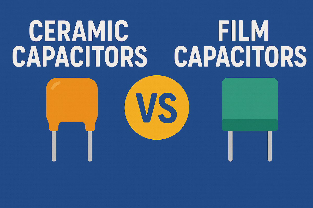 Ceramic Capacitors vs Film Capacitors: A Comprehensive Comparison Guide
14 May 20255646
 Introduction to Optical Amplifier
27 March 20259977
 What is UWB (Ultra-wideband)?
04 June 20218336
 How 10k Resistor Color Code Stacks Up Against 220 and 100k
03 September 20254554
 AC Contactor: What is Self-Locking?
01 March 202212197
 Semiconductor Industry's Uphill Battle Towards Net Zero
22 September 20232091
 How to Use the Oscilloscope's X-Y Display Correctly
19 September 202215749
 STM32U5: The Most Complex Low-power MCU
19 January 202212362
Diodes Incorporated
In Stock: 27388
United States
China
Canada
Japan
Russia
Germany
United Kingdom
Singapore
Italy
Hong Kong(China)
Taiwan(China)
France
Korea
Mexico
Netherlands
Malaysia
Austria
Spain
Switzerland
Poland
Thailand
Vietnam
India
United Arab Emirates
Afghanistan
Åland Islands
Albania
Algeria
American Samoa
Andorra
Angola
Anguilla
Antigua & Barbuda
Argentina
Armenia
Aruba
Australia
Azerbaijan
Bahamas
Bahrain
Bangladesh
Barbados
Belarus
Belgium
Belize
Benin
Bermuda
Bhutan
Bolivia
Bonaire, Sint Eustatius and Saba
Bosnia & Herzegovina
Botswana
Brazil
British Indian Ocean Territory
British Virgin Islands
Brunei
Bulgaria
Burkina Faso
Burundi
Cabo Verde
Cambodia
Cameroon
Cayman Islands
Central African Republic
Chad
Chile
Christmas Island
Cocos (Keeling) Islands
Colombia
Comoros
Congo
Congo (DRC)
Cook Islands
Costa Rica
Côte d’Ivoire
Croatia
Cuba
Curaçao
Cyprus
Czechia
Denmark
Djibouti
Dominica
Dominican Republic
Ecuador
Egypt
El Salvador
Equatorial Guinea
Eritrea
Estonia
Eswatini
Ethiopia
Falkland Islands
Faroe Islands
Fiji
Finland
French Guiana
French Polynesia
Gabon
Gambia
Georgia
Ghana
Gibraltar
Greece
Greenland
Grenada
Guadeloupe
Guam
Guatemala
Guernsey
Guinea
Guinea-Bissau
Guyana
Haiti
Honduras
Hungary
Iceland
Indonesia
Iran
Iraq
Ireland
Isle of Man
Israel
Jamaica
Jersey
Jordan
Kazakhstan
Kenya
Kiribati
Kosovo
Kuwait
Kyrgyzstan
Laos
Latvia
Lebanon
Lesotho
Liberia
Libya
Liechtenstein
Lithuania
Luxembourg
Macao(China)
Madagascar
Malawi
Maldives
Mali
Malta
Marshall Islands
Martinique
Mauritania
Mauritius
Mayotte
Micronesia
Moldova
Monaco
Mongolia
Montenegro
Montserrat
Morocco
Mozambique
Myanmar
Namibia
Nauru
Nepal
New Caledonia
New Zealand
Nicaragua
Niger
Nigeria
Niue
Norfolk Island
North Korea
North Macedonia
Northern Mariana Islands
Norway
Oman
Pakistan
Palau
Palestinian Authority
Panama
Papua New Guinea
Paraguay
Peru
Philippines
Pitcairn Islands
Portugal
Puerto Rico
Qatar
Réunion
Romania
Rwanda
Samoa
San Marino
São Tomé & Príncipe
Saudi Arabia
Senegal
Serbia
Seychelles
Sierra Leone
Sint Maarten
Slovakia
Slovenia
Solomon Islands
Somalia
South Africa
South Sudan
Sri Lanka
St Helena, Ascension, Tristan da Cunha
St. Barthélemy
St. Kitts & Nevis
St. Lucia
St. Martin
St. Pierre & Miquelon
St. Vincent & Grenadines
Sudan
Suriname
Svalbard & Jan Mayen
Sweden
Syria
Tajikistan
Tanzania
Timor-Leste
Togo
Tokelau
Tonga
Trinidad & Tobago
Tunisia
Turkey
Turkmenistan
Turks & Caicos Islands
Tuvalu
U.S. Outlying Islands
U.S. Virgin Islands
Uganda
Ukraine
Uruguay
Uzbekistan
Vanuatu
Vatican City
Venezuela
Wallis & Futuna
Yemen
Zambia
Zimbabwe
![DMG1012T-7]() DMG1012T-7
DMG1012T-7Diodes Incorporated
![BSS138-7-F]() BSS138-7-F
BSS138-7-FDiodes Incorporated
![BSS123W-7-F]() BSS123W-7-F
BSS123W-7-FDiodes Incorporated
![BSS84W-7-F]() BSS84W-7-F
BSS84W-7-FDiodes Incorporated
![BSS123-7-F]() BSS123-7-F
BSS123-7-FDiodes Incorporated
![BSS138W-7-F]() BSS138W-7-F
BSS138W-7-FDiodes Incorporated
![2N7002W-7-F]() 2N7002W-7-F
2N7002W-7-FDiodes Incorporated
![MMBF170-7-F]() MMBF170-7-F
MMBF170-7-FDiodes Incorporated
![ZXMP10A13FTA]() ZXMP10A13FTA
ZXMP10A13FTADiodes Incorporated
![DMG1013T-7]() DMG1013T-7
DMG1013T-7Diodes Incorporated


