
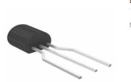
J113 N-Channel Switch: J113 Transistor Equivalents and Datasheet


JFET N-CH 35V 625MW TO92
J113 is a J11x series N Channel silicon FET or field-effect transistor. J111 and J112 are two more transistors in this family. This article is going to cover datasheet, pinout, equivalents about J113 transistor.

Mega 328 medida de jfet TESTER J201 2N5457 J112 J111 J113
What is J113?
J113 is a J11x series N Channel silicon FET or field-effect transistor. J111 and J112 are two more transistors in this family. TO-92 and SOT-23 packaging are available for the transistors.
They're primarily employed in choppers, sample and hold applications, current limiting applications, switching applications, commentators, and other similar applications.
J113 Pinout

J113 Pinout
J113 CAD Model

J113 Symbol
J113 Footprint

J113 3D Model
Specifications
- TypeParameter
- Mounting Type
The "Mounting Type" in electronic components refers to the method used to attach or connect a component to a circuit board or other substrate, such as through-hole, surface-mount, or panel mount.
Through Hole - Package / Case
refers to the protective housing that encases an electronic component, providing mechanical support, electrical connections, and thermal management.
TO-226-3, TO-92-3 (TO-226AA) (Formed Leads) - Supplier Device Package
The parameter "Supplier Device Package" in electronic components refers to the physical packaging or housing of the component as provided by the supplier. It specifies the form factor, dimensions, and layout of the component, which are crucial for compatibility and integration into electronic circuits and systems. The supplier device package information typically includes details such as the package type (e.g., DIP, SOP, QFN), number of pins, pitch, and overall size, allowing engineers and designers to select the appropriate component for their specific application requirements. Understanding the supplier device package is essential for proper component selection, placement, and soldering during the manufacturing process to ensure optimal performance and reliability of the electronic system.
TO-92-3 - Operating Temperature
The operating temperature is the range of ambient temperature within which a power supply, or any other electrical equipment, operate in. This ranges from a minimum operating temperature, to a peak or maximum operating temperature, outside which, the power supply may fail.
-55°C~150°C TJ - Packaging
Semiconductor package is a carrier / shell used to contain and cover one or more semiconductor components or integrated circuits. The material of the shell can be metal, plastic, glass or ceramic.
Tape & Box (TB) - Part Status
Parts can have many statuses as they progress through the configuration, analysis, review, and approval stages.
Obsolete - Moisture Sensitivity Level (MSL)
Moisture Sensitivity Level (MSL) is a standardized rating that indicates the susceptibility of electronic components, particularly semiconductors, to moisture-induced damage during storage and the soldering process, defining the allowable exposure time to ambient conditions before they require special handling or baking to prevent failures
1 (Unlimited) - Base Part Number
The "Base Part Number" (BPN) in electronic components serves a similar purpose to the "Base Product Number." It refers to the primary identifier for a component that captures the essential characteristics shared by a group of similar components. The BPN provides a fundamental way to reference a family or series of components without specifying all the variations and specific details.
J113 - Power - Max
Power - Max is a parameter that specifies the maximum amount of power that an electronic component can handle without being damaged. It is typically measured in watts and indicates the upper limit of power that can be safely supplied to the component. Exceeding the maximum power rating can lead to overheating, malfunction, or permanent damage to the component. It is important to consider the power-max rating when designing circuits or systems to ensure proper operation and longevity of the electronic components.
625mW - FET Type
"FET Type" refers to the type of Field-Effect Transistor (FET) being used in an electronic component. FETs are three-terminal semiconductor devices that can be classified into different types based on their construction and operation. The main types of FETs include Metal-Oxide-Semiconductor FETs (MOSFETs), Junction FETs (JFETs), and Insulated-Gate Bipolar Transistors (IGBTs).Each type of FET has its own unique characteristics and applications. MOSFETs are commonly used in digital circuits due to their high input impedance and low power consumption. JFETs are often used in low-noise amplifiers and switching circuits. IGBTs combine the high input impedance of MOSFETs with the high current-carrying capability of bipolar transistors, making them suitable for high-power applications like motor control and power inverters.When selecting an electronic component, understanding the FET type is crucial as it determines the device's performance and suitability for a specific application. It is important to consider factors such as voltage ratings, current handling capabilities, switching speeds, and power dissipation when choosing the right FET type for a particular circuit design.
N-Channel - Current - Drain (Idss) @ Vds (Vgs=0)
The parameter "Current - Drain (Idss) @ Vds (Vgs=0)" in electronic components refers to the maximum drain current that flows through the device when the gate-source voltage (Vgs) is zero. This parameter is typically specified for field-effect transistors (FETs) and is an important characteristic that indicates the device's maximum current-carrying capacity in the off state. It helps in determining the saturation current of the FET and is crucial for designing circuits where high current handling capability is required. Manufacturers provide this parameter in the datasheet of the component to assist engineers and designers in selecting the appropriate component for their applications.
2mA @ 15V - Voltage - Cutoff (VGS off) @ Id
Voltage - Cutoff (VGS off) @ Id refers to the gate-source voltage at which a field-effect transistor (FET) or similar device ceases to conduct, effectively turning it off. This parameter indicates the threshold voltage that separates the conducting state from the cutoff state for a specified drain current (Id). It is crucial for determining the operating characteristics of the device in various applications, ensuring efficient switching and control in electronic circuits.
500mV @ 1μA - Voltage - Breakdown (V(BR)GSS)
Voltage - Breakdown (V(BR)GSS) is a parameter used to describe the maximum gate-source voltage that can be applied to a field-effect transistor (FET) without causing a breakdown in the gate-source junction. This parameter is crucial in determining the safe operating limits of the FET and helps prevent damage to the component. When the gate-source voltage exceeds the breakdown voltage, it can lead to a sudden increase in current flow and potentially damage the FET. Therefore, understanding and adhering to the specified V(BR)GSS value is essential for proper functioning and reliability of electronic circuits utilizing FETs.
35V - Resistance - RDS(On)
Resistance - RDS(On) refers to the on-state resistance of a MOSFET when it is fully turned on. It is a critical parameter that indicates the resistance between the drain and source terminals of the device in the conducting state. Lower RDS(On) values result in reduced power loss and heat generation during operation, making it an important specification for efficiency in electronic circuits. It is typically measured in ohms and is a key consideration in the selection of transistors for power applications.
100Ohms
J113 Features
Package-Type: TO-92 , SOT-23
Transistor Type: N Channel JFET (Symmetrical)
Maximum Drain to Gate Voltage: 35V
Maximum Reverse Gate to Source Voltage: –35V
Maximum Continues Gate Current: 50mA
Maximum Gate to Source Cutoff Voltage: –5 to –3V
Maximum Power Dissipation: 625mW
Max Storage & Operating temperature should be: -55 to +150 °C
Drain and source are exchangeable
Benefits of J113
High switching speed
Better response to the frequency
Good accuracy
Low cost
Low insertion loss etc.
J113 Applications
Audio preamplifiers
High gain amplifiers
Sensor & detector circuits
Current limiting circuits
Analog switching circuits
Low-level signal amplification
Where and How to use J113?
J113 is suitable for a wide range of applications, including current limiting, chopper, and a variety of analog switching circuits. Aside from that, it can be used to boost the strength of any form of electronic signal in high gain amplifier applications.
Equivalents for J113
| Part No. | Manufacturer/Description |
| J111 | RF FET Transistor, 35 V, 625 mW, TO-92 ON SEMI |
| J112 | ON SEMI JFET Transistor, -35 V, 5 mA, -5 V, TO-92, JFET Each |
J113 Dimension Outline


J113 Dimension Outline
J113 Manufacturer
onsemi (formerly ON Semiconductor until August 5, 2021) is an American semiconductor supplier company, formerly in the Fortune 500, but dropping into the Fortune 1000 (ranked 512) in 2020.[3][1] Products include power and signal management, logic, discrete, and custom devices for automotive, communications, computing, consumer, industrial, LED lighting, medical, military/aerospace and power applications.
What is J113 used for?
The J113 is a through-hole, N-channel switch in the TO-92 package. This device is designed for low-level analog switching, sample and holds circuits, and chopper stabilized amplifiers.
What is the voltage of j113?
Its supply voltage DC max is 30V.
What is the operating temperature of J113?
-55°C~150°C TJ
How does a JFET work?
A JFET is a three-terminal semiconductor device that uses one type of carriers, such as electrons or holes, to conduct current. The device's current conduction is controlled by an electric field that exists between the gate and the conducting channel. The JFET has a low noise level and a high input impedance.
![BTA16 Triacs: Features, Pinout, and Datasheet [Video&FAQ]](https://res.utmel.com/Images/Article/90a7e9a1-f4df-4f46-861a-0e4e514ca8a2.png) BTA16 Triacs: Features, Pinout, and Datasheet [Video&FAQ]
BTA16 Triacs: Features, Pinout, and Datasheet [Video&FAQ]10 January 202215185
 S9015 PNP Transistor: Low Frequency, Low Noise TO-92 S9015 Equivalents and Circuit
18 January 202211617
 A Comprehensive Guide to Fairchild 74ACTQ16245SSC Bus Transceiver
11 March 2024427
 S9012 Transistor: BJT Transistor, Datasheet, Equivalent
17 January 20227955
 STM32F407VGT6 Microcontroller: 168MHz,100-LQFP, Pinout and Features
07 February 202211370
 TB6600 Stepper Motor Driver IC: Schematci, Price and Datasheet
20 July 20219907
 STM32F103C8T6 Microcontroller: Pinout, Datasheet, and Circuit
14 July 202118095
 Getting Started with STM32F756ZG Microcontroller Programming
15 July 2025252
 Surge Protector Best Practices for Everyday Use
10 July 2025495
 What is UART(Universal Asynchronous Receiver And Transmitter) ?
25 September 20216022
 Comparative Analysis of Si and SiC Devices for EV Traction Inverters
10 March 20233169
 Adopting GaN/Si MMIC in Space-based Applications
14 June 20242263
 The Introduction of Car Fuse
09 October 20214579
![Comprehensive Guide to Car Chips [FAQs]](https://res.utmel.com/Images/Article/e686e156-9363-4bbc-b1fd-c44fbe3ecbda.jpg) Comprehensive Guide to Car Chips [FAQs]
Comprehensive Guide to Car Chips [FAQs]11 January 20225186
 Why Precision Matters in Analog-to-Digital Conversion
28 May 2025363
 Basic Introduction to System on a Chip
02 December 20203527
ON Semiconductor
In Stock
United States
China
Canada
Japan
Russia
Germany
United Kingdom
Singapore
Italy
Hong Kong(China)
Taiwan(China)
France
Korea
Mexico
Netherlands
Malaysia
Austria
Spain
Switzerland
Poland
Thailand
Vietnam
India
United Arab Emirates
Afghanistan
Åland Islands
Albania
Algeria
American Samoa
Andorra
Angola
Anguilla
Antigua & Barbuda
Argentina
Armenia
Aruba
Australia
Azerbaijan
Bahamas
Bahrain
Bangladesh
Barbados
Belarus
Belgium
Belize
Benin
Bermuda
Bhutan
Bolivia
Bonaire, Sint Eustatius and Saba
Bosnia & Herzegovina
Botswana
Brazil
British Indian Ocean Territory
British Virgin Islands
Brunei
Bulgaria
Burkina Faso
Burundi
Cabo Verde
Cambodia
Cameroon
Cayman Islands
Central African Republic
Chad
Chile
Christmas Island
Cocos (Keeling) Islands
Colombia
Comoros
Congo
Congo (DRC)
Cook Islands
Costa Rica
Côte d’Ivoire
Croatia
Cuba
Curaçao
Cyprus
Czechia
Denmark
Djibouti
Dominica
Dominican Republic
Ecuador
Egypt
El Salvador
Equatorial Guinea
Eritrea
Estonia
Eswatini
Ethiopia
Falkland Islands
Faroe Islands
Fiji
Finland
French Guiana
French Polynesia
Gabon
Gambia
Georgia
Ghana
Gibraltar
Greece
Greenland
Grenada
Guadeloupe
Guam
Guatemala
Guernsey
Guinea
Guinea-Bissau
Guyana
Haiti
Honduras
Hungary
Iceland
Indonesia
Iran
Iraq
Ireland
Isle of Man
Israel
Jamaica
Jersey
Jordan
Kazakhstan
Kenya
Kiribati
Kosovo
Kuwait
Kyrgyzstan
Laos
Latvia
Lebanon
Lesotho
Liberia
Libya
Liechtenstein
Lithuania
Luxembourg
Macao(China)
Madagascar
Malawi
Maldives
Mali
Malta
Marshall Islands
Martinique
Mauritania
Mauritius
Mayotte
Micronesia
Moldova
Monaco
Mongolia
Montenegro
Montserrat
Morocco
Mozambique
Myanmar
Namibia
Nauru
Nepal
New Caledonia
New Zealand
Nicaragua
Niger
Nigeria
Niue
Norfolk Island
North Korea
North Macedonia
Northern Mariana Islands
Norway
Oman
Pakistan
Palau
Palestinian Authority
Panama
Papua New Guinea
Paraguay
Peru
Philippines
Pitcairn Islands
Portugal
Puerto Rico
Qatar
Réunion
Romania
Rwanda
Samoa
San Marino
São Tomé & Príncipe
Saudi Arabia
Senegal
Serbia
Seychelles
Sierra Leone
Sint Maarten
Slovakia
Slovenia
Solomon Islands
Somalia
South Africa
South Sudan
Sri Lanka
St Helena, Ascension, Tristan da Cunha
St. Barthélemy
St. Kitts & Nevis
St. Lucia
St. Martin
St. Pierre & Miquelon
St. Vincent & Grenadines
Sudan
Suriname
Svalbard & Jan Mayen
Sweden
Syria
Tajikistan
Tanzania
Timor-Leste
Togo
Tokelau
Tonga
Trinidad & Tobago
Tunisia
Turkey
Turkmenistan
Turks & Caicos Islands
Tuvalu
U.S. Outlying Islands
U.S. Virgin Islands
Uganda
Ukraine
Uruguay
Uzbekistan
Vanuatu
Vatican City
Venezuela
Wallis & Futuna
Yemen
Zambia
Zimbabwe
![MMBFJ177LT1G]() MMBFJ177LT1G
MMBFJ177LT1GON Semiconductor
![MMBFJ201]() MMBFJ201
MMBFJ201ON Semiconductor
![MMBFJ108]() MMBFJ108
MMBFJ108ON Semiconductor
![MMBF4391LT1G]() MMBF4391LT1G
MMBF4391LT1GON Semiconductor
![MMBF4393LT1G]() MMBF4393LT1G
MMBF4393LT1GON Semiconductor
![MMBFJ175]() MMBFJ175
MMBFJ175ON Semiconductor
![MMBFJ175LT1G]() MMBFJ175LT1G
MMBFJ175LT1GON Semiconductor
![MMBF4392LT1G]() MMBF4392LT1G
MMBF4392LT1GON Semiconductor
![MMBFJ202]() MMBFJ202
MMBFJ202ON Semiconductor
![J175-D26Z]() J175-D26Z
J175-D26ZON Semiconductor


