
 Product
 Brand
Brand Articles
 Tools
Tools
MCP1253 DC/DC Converter: Specifications, Pinout and Datasheet

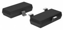
8 Terminals 2.7V 8-Pin MCP1253 DC DC Voltage Regulator SWITCHED CAPACITOR REGULATOR 1 Outputs Tube 8-TSSOP, 8-MSOP (0.118, 3.00mm Width)


8 Terminals 2.7V 8-Pin MCP1253 DC DC Voltage Regulator SWITCHED CAPACITOR REGULATOR 1 Outputs Tube 8-TSSOP, 8-MSOP (0.118, 3.00mm Width)
The MCP1253 is inductorless, positive-regulated charge pump DC/DC converter. The device generate a regulated fixed (3.3V or 5.0V) or adjustable output voltage. Furthermore, Huge range of Semiconductors, Capacitors, Resistors and IcS in stock. Welcome RFQ.
Description
The MCP1253 is inductorless, positive-regulated charge pump DC/DC converter. The device generates a regulated fixed (3.3V or 5.0V) or adjustable output voltage. It is specifically designed for applications requiring low noise and high efficiency and is able to deliver up to 120 mA output current. The device allows the input voltage to be lower or higher than the output voltage, by automatically switching between buck/boost operation. The MCP1253 has a switching frequency of 1 MHz and allows the use of smaller capacitors than the MCP1252, thus saving board space and cost.
MCP1253 Pinout

MCP1253 Pinout

Pin Function Table
MCP1253 CAD Model

Symbol

Footprint

3D-Model
MCP1253 Features
• Inductorless, Buck/Boost, DC/DC Converter
• Low Power: 80 µA (Typical)
• High Output Voltage Accuracy:
- ±2.5% (VOUT Fixed)
• 120 mA Output Current
• Wide Operating Temperature Range:
- Industrial Temperature (I): -40°C to +85°C
- Extended Temperature (E): -40°C to +125°C
• Thermal Shutdown and Short-Circuit Protection
• Uses Small Ceramic Capacitors
• Switching Frequency:
- MCP1252: 650 kHz
- MCP1253: 1 MHz
• Low-Power Shutdown Mode: 0.1 µA (Typical)
• Shutdown Input Compatible with 1.8V Logic
• VIN Range: 2.0V to 5.5V
• Selectable Output Voltage (3.3V or 5.0V) or Adjustable Output Voltage
• Space-Saving, 8-Lead MSOP
• Soft-Start Circuitry to Minimize In-Rush Current
• AEC-Q100 Qualified
MCP1253 Advantage
The MCP1253 has a switching frequency of 1 MHz and allows the use of smaller capacitors than the MCP1252, thus saving board space and cost. The device features a power-good output that can be used to detect out-of-regulation conditions. Extremely low supply current and low external parts count (three capacitors) make the device ideal for small, batterypowered applications. A shutdown mode is also provided for further power reduction. The MCP1253 features thermal and short-circuit protection and are offered in space-saving, 8-lead, MSOP package.
Specifications
- TypeParameter
- Factory Lead Time16 Weeks
- Mount
In electronic components, the term "Mount" typically refers to the method or process of physically attaching or fixing a component onto a circuit board or other electronic device. This can involve soldering, adhesive bonding, or other techniques to secure the component in place. The mounting process is crucial for ensuring proper electrical connections and mechanical stability within the electronic system. Different components may have specific mounting requirements based on their size, shape, and function, and manufacturers provide guidelines for proper mounting procedures to ensure optimal performance and reliability of the electronic device.
Surface Mount - Mounting Type
The "Mounting Type" in electronic components refers to the method used to attach or connect a component to a circuit board or other substrate, such as through-hole, surface-mount, or panel mount.
Surface Mount - Package / Case
refers to the protective housing that encases an electronic component, providing mechanical support, electrical connections, and thermal management.
8-TSSOP, 8-MSOP (0.118, 3.00mm Width) - Number of Pins8
- Weight139.989945mg
- Usage LevelIndustrial grade
- Operating Temperature
The operating temperature is the range of ambient temperature within which a power supply, or any other electrical equipment, operate in. This ranges from a minimum operating temperature, to a peak or maximum operating temperature, outside which, the power supply may fail.
-40°C~85°C TA - Packaging
Semiconductor package is a carrier / shell used to contain and cover one or more semiconductor components or integrated circuits. The material of the shell can be metal, plastic, glass or ceramic.
Tube - Published2002
- JESD-609 Code
The "JESD-609 Code" in electronic components refers to a standardized marking code that indicates the lead-free solder composition and finish of electronic components for compliance with environmental regulations.
e3 - Pbfree Code
The "Pbfree Code" parameter in electronic components refers to the code or marking used to indicate that the component is lead-free. Lead (Pb) is a toxic substance that has been widely used in electronic components for many years, but due to environmental concerns, there has been a shift towards lead-free alternatives. The Pbfree Code helps manufacturers and users easily identify components that do not contain lead, ensuring compliance with regulations and promoting environmentally friendly practices. It is important to pay attention to the Pbfree Code when selecting electronic components to ensure they meet the necessary requirements for lead-free applications.
yes - Part Status
Parts can have many statuses as they progress through the configuration, analysis, review, and approval stages.
Active - Moisture Sensitivity Level (MSL)
Moisture Sensitivity Level (MSL) is a standardized rating that indicates the susceptibility of electronic components, particularly semiconductors, to moisture-induced damage during storage and the soldering process, defining the allowable exposure time to ambient conditions before they require special handling or baking to prevent failures
1 (Unlimited) - Number of Terminations8
- ECCN Code
An ECCN (Export Control Classification Number) is an alphanumeric code used by the U.S. Bureau of Industry and Security to identify and categorize electronic components and other dual-use items that may require an export license based on their technical characteristics and potential for military use.
EAR99 - Terminal Finish
Terminal Finish refers to the surface treatment applied to the terminals or leads of electronic components to enhance their performance and longevity. It can improve solderability, corrosion resistance, and overall reliability of the connection in electronic assemblies. Common finishes include nickel, gold, and tin, each possessing distinct properties suitable for various applications. The choice of terminal finish can significantly impact the durability and effectiveness of electronic devices.
Matte Tin (Sn) - annealed - Terminal Position
In electronic components, the term "Terminal Position" refers to the physical location of the connection points on the component where external electrical connections can be made. These connection points, known as terminals, are typically used to attach wires, leads, or other components to the main body of the electronic component. The terminal position is important for ensuring proper connectivity and functionality of the component within a circuit. It is often specified in technical datasheets or component specifications to help designers and engineers understand how to properly integrate the component into their circuit designs.
DUAL - Terminal Form
Occurring at or forming the end of a series, succession, or the like; closing; concluding.
GULL WING - Peak Reflow Temperature (Cel)
Peak Reflow Temperature (Cel) is a parameter that specifies the maximum temperature at which an electronic component can be exposed during the reflow soldering process. Reflow soldering is a common method used to attach electronic components to a circuit board. The Peak Reflow Temperature is crucial because it ensures that the component is not damaged or degraded during the soldering process. Exceeding the specified Peak Reflow Temperature can lead to issues such as component failure, reduced performance, or even permanent damage to the component. It is important for manufacturers and assemblers to adhere to the recommended Peak Reflow Temperature to ensure the reliability and functionality of the electronic components.
260 - Terminal Pitch
The center distance from one pole to the next.
0.65mm - Current Rating
Current rating is the maximum current that a fuse will carry for an indefinite period without too much deterioration of the fuse element.
80A - Frequency
In electronic components, the parameter "Frequency" refers to the rate at which a signal oscillates or cycles within a given period of time. It is typically measured in Hertz (Hz) and represents how many times a signal completes a full cycle in one second. Frequency is a crucial aspect in electronic components as it determines the behavior and performance of various devices such as oscillators, filters, and communication systems. Understanding the frequency characteristics of components is essential for designing and analyzing electronic circuits to ensure proper functionality and compatibility with other components in a system.
1MHz - Time@Peak Reflow Temperature-Max (s)
Time@Peak Reflow Temperature-Max (s) refers to the maximum duration that an electronic component can be exposed to the peak reflow temperature during the soldering process, which is crucial for ensuring reliable solder joint formation without damaging the component.
40 - Base Part Number
The "Base Part Number" (BPN) in electronic components serves a similar purpose to the "Base Product Number." It refers to the primary identifier for a component that captures the essential characteristics shared by a group of similar components. The BPN provides a fundamental way to reference a family or series of components without specifying all the variations and specific details.
MCP1253 - Function
The parameter "Function" in electronic components refers to the specific role or purpose that the component serves within an electronic circuit. It defines how the component interacts with other elements, influences the flow of electrical signals, and contributes to the overall behavior of the system. Functions can include amplification, signal processing, switching, filtering, and energy storage, among others. Understanding the function of each component is essential for designing effective and efficient electronic systems.
Step-Up/Step-Down - Number of Outputs1
- Output Voltage
Output voltage is a crucial parameter in electronic components that refers to the voltage level produced by the component as a result of its operation. It represents the electrical potential difference between the output terminal of the component and a reference point, typically ground. The output voltage is a key factor in determining the performance and functionality of the component, as it dictates the level of voltage that will be delivered to the connected circuit or load. It is often specified in datasheets and technical specifications to ensure compatibility and proper functioning within a given system.
5V - Output Type
The "Output Type" parameter in electronic components refers to the type of signal or data that is produced by the component as an output. This parameter specifies the nature of the output signal, such as analog or digital, and can also include details about the voltage levels, current levels, frequency, and other characteristics of the output signal. Understanding the output type of a component is crucial for ensuring compatibility with other components in a circuit or system, as well as for determining how the output signal can be utilized or processed further. In summary, the output type parameter provides essential information about the nature of the signal that is generated by the electronic component as its output.
Programmable - Max Output Current
The maximum current that can be supplied to the load.
120mA - Voltage - Input (Min)
Voltage - Input (Min) refers to the minimum voltage level that an electronic component requires to operate correctly. It indicates the lowest voltage that can be applied to the component while still allowing it to function as intended. If the input voltage falls below this specified minimum, the component may not perform properly or may fail to operate altogether. This parameter is critical for ensuring reliable operation and longevity of the device in electronic circuits.
2.7V - Input Voltage-Nom
Input Voltage-Nom refers to the nominal or rated input voltage that an electronic component or device is designed to operate within. This parameter specifies the voltage level at which the component is expected to function optimally and safely. It is important to ensure that the actual input voltage supplied to the component does not exceed this nominal value to prevent damage or malfunction. Manufacturers provide this specification to guide users in selecting the appropriate power supply or input voltage source for the component. It is a critical parameter to consider when designing or using electronic circuits to ensure reliable performance and longevity of the component.
3.6V - Max Supply Voltage
In general, the absolute maximum common-mode voltage is VEE-0.3V and VCC+0.3V, but for products without a protection element at the VCC side, voltages up to the absolute maximum rated supply voltage (i.e. VEE+36V) can be supplied, regardless of supply voltage.
5.5V - Min Supply Voltage
The minimum supply voltage (V min ) is explored for sequential logic circuits by statistically simulating the impact of within-die process variations and gate-dielectric soft breakdown on data retention and hold time.
2.1V - Analog IC - Other Type
Analog IC - Other Type is a parameter used to categorize electronic components that are integrated circuits (ICs) designed for analog signal processing but do not fall into more specific subcategories such as amplifiers, comparators, or voltage regulators. These ICs may include specialized analog functions such as analog-to-digital converters (ADCs), digital-to-analog converters (DACs), voltage references, or signal conditioning circuits. They are typically used in various applications where precise analog signal processing is required, such as in audio equipment, instrumentation, communication systems, and industrial control systems. Manufacturers provide detailed specifications for these components to help engineers select the most suitable IC for their specific design requirements.
SWITCHED CAPACITOR REGULATOR - Output Configuration
Output Configuration in electronic components refers to the arrangement or setup of the output pins or terminals of a device. It defines how the output signals are structured and how they interact with external circuits or devices. The output configuration can determine the functionality and compatibility of the component in a circuit design. Common types of output configurations include single-ended, differential, open-drain, and push-pull configurations, each serving different purposes and applications in electronic systems. Understanding the output configuration of a component is crucial for proper integration and operation within a circuit.
Positive - Voltage - Output (Min/Fixed)
Voltage - Output (Min/Fixed) refers to the minimum fixed output voltage level that an electronic component, such as a voltage regulator or power supply, is designed to provide under specified load conditions. This parameter ensures that the device consistently delivers a reliable voltage that meets the requirements of the connected circuits or components. It is critical for applications where stable and predictable voltage is necessary for proper operation.
3.3V 5V - Topology
In the context of electronic components, "topology" refers to the arrangement or configuration of the components within a circuit or system. It defines how the components are connected to each other and how signals flow between them. The choice of topology can significantly impact the performance, efficiency, and functionality of the electronic system. Common topologies include series, parallel, star, mesh, and hybrid configurations, each with its own advantages and limitations. Designers carefully select the appropriate topology based on the specific requirements of the circuit to achieve the desired performance and functionality.
Charge Pump - Control Mode
In electronic components, "Control Mode" refers to the method or mode of operation used to regulate or control the behavior of the component. This parameter determines how the component responds to input signals or commands to achieve the desired output. The control mode can vary depending on the specific component and its intended function, such as voltage regulation, current limiting, or frequency modulation. Understanding the control mode of an electronic component is crucial for proper integration and operation within a circuit or system.
VOLTAGE-MODE - Control Technique
In electronic components, "Control Technique" refers to the method or approach used to regulate and manage the operation of the component. This parameter is crucial in determining how the component functions within a circuit or system. Different control techniques can include analog control, digital control, pulse-width modulation (PWM), and various feedback mechanisms. The choice of control technique can impact the performance, efficiency, and overall functionality of the electronic component. It is important to select the appropriate control technique based on the specific requirements and characteristics of the application in which the component will be used.
PULSE WIDTH MODULATION - Synchronous Rectifier
Synchronous rectification is a technique for improving the efficiency of rectification by replacing diodes with actively controlled switches, usually power MOSFETs or power bipolar junction transistors (BJT).
No - Switcher Configuration
Switcher Configuration in electronic components refers to the arrangement or setup of a switcher circuit, which is a type of power supply that converts one form of electrical energy into another. The configuration of a switcher circuit includes the specific components used, such as transistors, diodes, capacitors, and inductors, as well as their interconnections and control mechanisms. The switcher configuration determines the efficiency, voltage regulation, and other performance characteristics of the power supply. Different switcher configurations, such as buck, boost, buck-boost, and flyback, are used for various applications depending on the desired output voltage and current requirements. Understanding and selecting the appropriate switcher configuration is crucial in designing reliable and efficient power supply systems for electronic devices.
BUCK-BOOST - Nominal Output Voltage
Nominal Output Voltage refers to the specified or intended voltage level that an electronic component or device is designed to provide as output under normal operating conditions. It is a crucial parameter that indicates the expected voltage level that the component will deliver to the connected circuit or load. This value is typically specified by the manufacturer and is important for ensuring proper functionality and compatibility within a system. It is important to note that the actual output voltage may vary slightly due to factors such as load variations, temperature changes, and other environmental conditions.
3.3V - Height850μm
- Length3mm
- Width3mm
- REACH SVHC
The parameter "REACH SVHC" in electronic components refers to the compliance with the Registration, Evaluation, Authorization, and Restriction of Chemicals (REACH) regulation regarding Substances of Very High Concern (SVHC). SVHCs are substances that may have serious effects on human health or the environment, and their use is regulated under REACH to ensure their safe handling and minimize their impact.Manufacturers of electronic components need to declare if their products contain any SVHCs above a certain threshold concentration and provide information on the safe use of these substances. This information allows customers to make informed decisions about the potential risks associated with using the components and take appropriate measures to mitigate any hazards.Ensuring compliance with REACH SVHC requirements is essential for electronics manufacturers to meet regulatory standards, protect human health and the environment, and maintain transparency in their supply chain. It also demonstrates a commitment to sustainability and responsible manufacturing practices in the electronics industry.
No SVHC - RoHS Status
RoHS means “Restriction of Certain Hazardous Substances” in the “Hazardous Substances Directive” in electrical and electronic equipment.
ROHS3 Compliant - Lead Free
Lead Free is a term used to describe electronic components that do not contain lead as part of their composition. Lead is a toxic material that can have harmful effects on human health and the environment, so the electronics industry has been moving towards lead-free components to reduce these risks. Lead-free components are typically made using alternative materials such as silver, copper, and tin. Manufacturers must comply with regulations such as the Restriction of Hazardous Substances (RoHS) directive to ensure that their products are lead-free and environmentally friendly.
Lead Free
MCP1253 Functional Block Diagram

MCP1253 Functional Block Diagram
MCP1253 Device Overview
Theory of Operation
The MCP1252 and MCP1253 family of devices employ a switched capacitor charge pump to buck or boost an input supply voltage (VIN) to a regulated output voltage. The regulation control is hysteretic, otherwise referred to as a bang-bang control. The output is regulated around a fixed reference with some hysteresis. As a result, typically 50 mV of peak-to-peak ripple will be observed at the output independent of load current. The frequency of the output ripple, however, will be influenced heavily by the load current and output capacitance. The maximum frequency that will be observed is equal to the internal oscillator frequency. The devices automatically transition between buck or boost operation. This provides a low-cost, compact and simple solution for step-down/step-up DC/DC conversion. This is especially true for battery-operated applications that require a fixed output above or below the input.
Power Efficiency
The power efficiency is determined by the mode of operation. In boost mode, the efficiency is approximately half of a linear regulator. In buck mode, the efficiency is approximately equal to that of a linear regulator. The following formulas can be used to approximate the power efficiency with any significant amount of output current. At light loads, the quiescent current of the device must be taken into consideration.
Soft-Start and Short-Circuit Protection
The MCP1252 and MCP1253 feature foldback shortcircuit protection. This circuitry provides an internal soft-start function by limiting in-rush current during startup and also limits the output current to 200 mA (typical) if the output is shorted to GND. The internal soft-start circuitry requires approximately 300 µsec, typical with a 5V output, from either initial power-up or release from shutdown for the output voltage to be in regulation.
Thermal Shutdown
The MCP1252 and MCP1253 feature thermal shutdown with temperature hysteresis. When the die temperature exceeds 160°C, typically, the device shuts down. When the die cools by 15°C, typically, the device automatically turns back on. If high die temperature is caused by output overload and the load is not removed, the device will turn on and off, resulting in a pulse output.
MCP1253 Application
• White LED Backlighting
• Color Display Bias
• Local 3V-to-5V Conversions
• Flash Memory Supply Voltage
• SIM Interface Supply for GSM Phones
• Smart Card Readers
• PCMCIA Local 5V Supplies
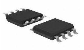
MCP1253 Package
![MCP1253 8-Lead Plastic Micro Small Outline Package (MS)[MSOP]TOP VIEW.png](https://res.utmel.com/Images/UEditor/3c6d2490-544a-473c-b754-e19b1b86d65e.png "MCP1253 8-Lead Plastic Micro Small Outline Package (MS)[MSOP]TOP VIEW.png")
top view
![MCP1253 8-Lead Plastic Micro Small Outline Package (MS)[MSOP] SIDE VIEW.png](https://res.utmel.com/Images/UEditor/08006410-b265-4468-b7ff-aabc7d0f4687.png "MCP1253 8-Lead Plastic Micro Small Outline Package (MS)[MSOP] SIDE VIEW.png")
side view
![MCP1253 8-Lead Plastic Micro Small Outline Package (MS)[MSOP] END VIEW.png](https://res.utmel.com/Images/UEditor/5e431853-089e-4553-8e21-e1a2a5370084.png "MCP1253 8-Lead Plastic Micro Small Outline Package (MS)[MSOP] END VIEW.png")
end view

Package marking

Package marking
Parts with Similar Specs
- ImagePart NumberManufacturerPackage / CaseNumber of PinsNumber of OutputsMax Output CurrentInput Voltage-NomVoltage - Input (Min)Nominal Output VoltageOutput VoltageView Compare
![MCP1253-33X50I/MS]()
MCP1253-33X50I/MS
8-TSSOP, 8-MSOP (0.118, 3.00mm Width)
8
1
120 mA
3.6 V
2.7V
3.3 V
5 V
![TPS62008DGS]()
10-TFSOP, 10-MSOP (0.118, 3.00mm Width)
10
1
600 mA
3.6 V
2.5V
1.2 V
1.2 V
![TPS62004DGSR]()
10-TFSOP, 10-MSOP (0.118, 3.00mm Width)
10
1
600 mA
3.6 V
2.5V
1.5 V
1.5 V
![NCP1421DMR2G]()
8-TSSOP, 8-MSOP (0.118, 3.00mm Width)
8
1
600 mA
3.3 V
1V
-
5 V
![TPS62003DGSR]()
10-TFSOP, 10-MSOP (0.118, 3.00mm Width)
10
1
600 mA
3.6 V
2.5V
-
1.9 V


MCP1253 Manufacturer
Microchip Technology Inc., is a leader that provides microcontroller and analog semiconductors. Microchip was headquartered in Chandler, Arizona. We are delicated to offering low-risk product development, reducing total system cost and accelerating time to market. We mainly serve for different fields of customers applications around the world. To provide prominent technical support along with reliable delivery and quality is our goal.
Trend Analysis
Datasheet PDF
- PCN Assembly/Origin :
- PCN Packaging :
- ConflictMineralStatement :
- Datasheets :
- PCN Design/Specification :
1. What is the nature of the MCP1253?
The MCP1253 is inductorless, positive-regulated charge pump DC/DC converter.
2. What is the product category of MCP1253?
Switching Voltage Regulators.
3. What is the package of MCP1253?
MSOP-8.
 BC817-40 NPN Transistor: Pinout, Equivalent and Datasheet
26 March 20225951
 BC338 NPN Transistor: Pinout, Datasheet, and Equivalents
25 August 20217142
![H1102NL How to use H1102NL?[FAQ&Video]](https://res.utmel.com/Images/Article/332ed242-9496-43e7-972e-bd59447bd7b2.png) H1102NL How to use H1102NL?[FAQ&Video]
H1102NL How to use H1102NL?[FAQ&Video]09 May 20225500
 A Comprehensive Guide to LTC6405IUD#PBF - ADC Driver Amplifier
06 March 2024157
 WM8960 Stereo CODEC: Pinout, Features and Datasheet
12 February 20226386
 LP2951 Voltage Regulator: Pinout, Equivalent and Datasheet
23 October 20213494
![STA8088EXG RF RX GALILEO 1.575GHZ 169TFBGA[FAQ]: Datasheet, Block Diagram, and Features](https://res.utmel.com/Images/Article/3fe63125-18b6-441c-8483-4490b58e8e35.jpg) STA8088EXG RF RX GALILEO 1.575GHZ 169TFBGA[FAQ]: Datasheet, Block Diagram, and Features
STA8088EXG RF RX GALILEO 1.575GHZ 169TFBGA[FAQ]: Datasheet, Block Diagram, and Features14 March 2022761
 Comparing STM32G474RET6 and STM32G474RCT6
24 July 20252450
 Car Sensors: Classification and Application
27 October 202513234
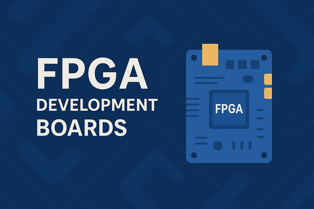 How to Simplify Intel FPGA Design with Development Boards
09 June 2025725
 Semiconductor Market Poised for Strong Rebound in 2024, Predicts WSTS
11 December 20235158
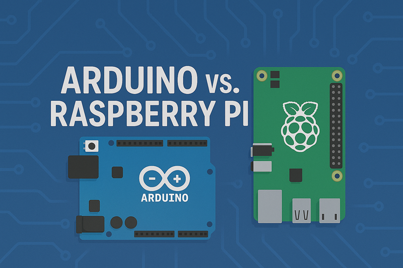 Arduino vs. Raspberry Pi: A Detailed Comparison
24 April 20255502
 What are Comparators?
03 December 20205949
 What is Low Pass Filter
18 November 20217238
 Methods for measuring the temperature of semiconductor devices
14 November 20222334
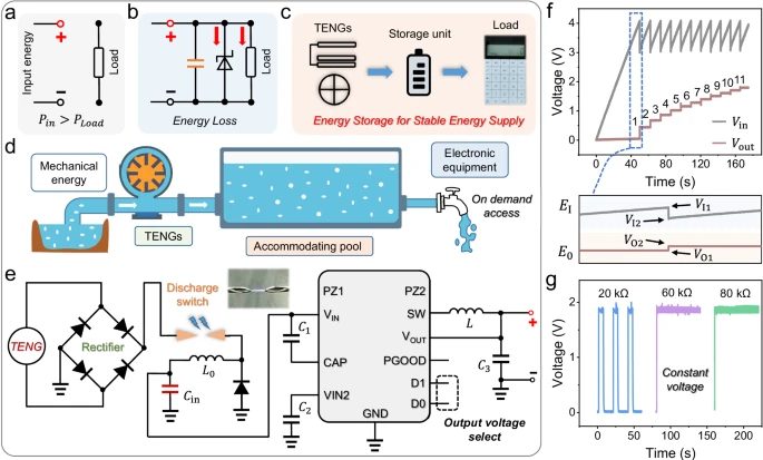 Improving the Energy Conversion Efficiency of Triboelectric Nanogenerators
19 November 20242985
Microchip Technology
In Stock
United States
China
Canada
Japan
Russia
Germany
United Kingdom
Singapore
Italy
Hong Kong(China)
Taiwan(China)
France
Korea
Mexico
Netherlands
Malaysia
Austria
Spain
Switzerland
Poland
Thailand
Vietnam
India
United Arab Emirates
Afghanistan
Åland Islands
Albania
Algeria
American Samoa
Andorra
Angola
Anguilla
Antigua & Barbuda
Argentina
Armenia
Aruba
Australia
Azerbaijan
Bahamas
Bahrain
Bangladesh
Barbados
Belarus
Belgium
Belize
Benin
Bermuda
Bhutan
Bolivia
Bonaire, Sint Eustatius and Saba
Bosnia & Herzegovina
Botswana
Brazil
British Indian Ocean Territory
British Virgin Islands
Brunei
Bulgaria
Burkina Faso
Burundi
Cabo Verde
Cambodia
Cameroon
Cayman Islands
Central African Republic
Chad
Chile
Christmas Island
Cocos (Keeling) Islands
Colombia
Comoros
Congo
Congo (DRC)
Cook Islands
Costa Rica
Côte d’Ivoire
Croatia
Cuba
Curaçao
Cyprus
Czechia
Denmark
Djibouti
Dominica
Dominican Republic
Ecuador
Egypt
El Salvador
Equatorial Guinea
Eritrea
Estonia
Eswatini
Ethiopia
Falkland Islands
Faroe Islands
Fiji
Finland
French Guiana
French Polynesia
Gabon
Gambia
Georgia
Ghana
Gibraltar
Greece
Greenland
Grenada
Guadeloupe
Guam
Guatemala
Guernsey
Guinea
Guinea-Bissau
Guyana
Haiti
Honduras
Hungary
Iceland
Indonesia
Iran
Iraq
Ireland
Isle of Man
Israel
Jamaica
Jersey
Jordan
Kazakhstan
Kenya
Kiribati
Kosovo
Kuwait
Kyrgyzstan
Laos
Latvia
Lebanon
Lesotho
Liberia
Libya
Liechtenstein
Lithuania
Luxembourg
Macao(China)
Madagascar
Malawi
Maldives
Mali
Malta
Marshall Islands
Martinique
Mauritania
Mauritius
Mayotte
Micronesia
Moldova
Monaco
Mongolia
Montenegro
Montserrat
Morocco
Mozambique
Myanmar
Namibia
Nauru
Nepal
New Caledonia
New Zealand
Nicaragua
Niger
Nigeria
Niue
Norfolk Island
North Korea
North Macedonia
Northern Mariana Islands
Norway
Oman
Pakistan
Palau
Palestinian Authority
Panama
Papua New Guinea
Paraguay
Peru
Philippines
Pitcairn Islands
Portugal
Puerto Rico
Qatar
Réunion
Romania
Rwanda
Samoa
San Marino
São Tomé & Príncipe
Saudi Arabia
Senegal
Serbia
Seychelles
Sierra Leone
Sint Maarten
Slovakia
Slovenia
Solomon Islands
Somalia
South Africa
South Sudan
Sri Lanka
St Helena, Ascension, Tristan da Cunha
St. Barthélemy
St. Kitts & Nevis
St. Lucia
St. Martin
St. Pierre & Miquelon
St. Vincent & Grenadines
Sudan
Suriname
Svalbard & Jan Mayen
Sweden
Syria
Tajikistan
Tanzania
Timor-Leste
Togo
Tokelau
Tonga
Trinidad & Tobago
Tunisia
Turkey
Turkmenistan
Turks & Caicos Islands
Tuvalu
U.S. Outlying Islands
U.S. Virgin Islands
Uganda
Ukraine
Uruguay
Uzbekistan
Vanuatu
Vatican City
Venezuela
Wallis & Futuna
Yemen
Zambia
Zimbabwe
![MCP16301T-I/CHY]() MCP16301T-I/CHY
MCP16301T-I/CHYMicrochip Technology
![MIC4680-5.0YM-TR]() MIC4680-5.0YM-TR
MIC4680-5.0YM-TRMicrochip Technology
![MCP16311-E/MS]() MCP16311-E/MS
MCP16311-E/MSMicrochip Technology
![MCP16331T-E/CH]() MCP16331T-E/CH
MCP16331T-E/CHMicrochip Technology
![TC7660SEOA]() TC7660SEOA
TC7660SEOAMicrochip Technology
![TC7660SEOA713]() TC7660SEOA713
TC7660SEOA713Microchip Technology
![TC7662BEOA713]() TC7662BEOA713
TC7662BEOA713Microchip Technology
![MIC4684YM]() MIC4684YM
MIC4684YMMicrochip Technology
![TC7662BEOA]() TC7662BEOA
TC7662BEOAMicrochip Technology
![MIC4680-5.0YM]() MIC4680-5.0YM
MIC4680-5.0YMMicrochip Technology

