

 Product
 Brand
Brand Articles
 Tools
Tools
LP5569RTWR 9 CHANNEL RGB DRIVER
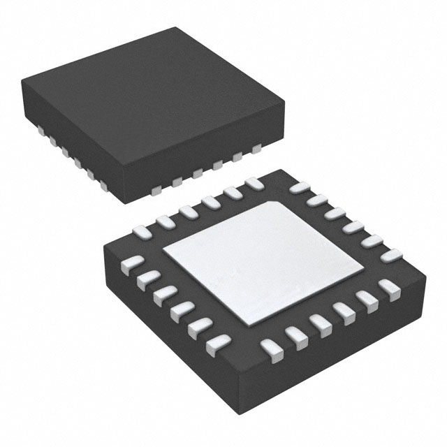


0.5mm PMIC LP5569 24 Pin 3.6V 24-WFQFN Exposed Pad
Texas Instruments LP5569RTWR I2C RGB LED Driver is a programmable, easy-to-use 9-channel I2C LED driver designed to produce lighting effects for various applications. This passage is going to introduce LP5569RTWR from the perspectives of the datasheet, pinout, and other ways.
- LP5569RTWR Description
- LP5569RTWR Pins and Pins Functions
- LP5569RTWR Feature
- LP5569RTWR CAD Models
- Specifications
- LP5569RTWR Applications
- LP5569RTWR Applications Circuit
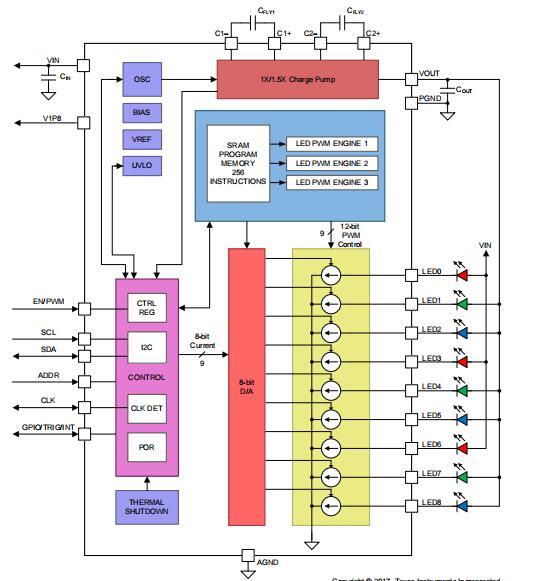
- LP5569RTWR Functional Block Diagram
- LP5569RTWR Manufacturer
- LP5569RTWR Package
- LP5569RTWR Advantages
- P5569RTWR Dimensions
- Trend Analysis
- Datasheet PDF
LP5569RTWR Description
The LP5569RTWR is a programmable, easy-to-use 9 -channel I2C LED driver that may be used to create various lighting effects. The LED driver includes an internal SRAM memory for user-programmed sequences as well as three programmable LED engines for operation without the usage of a processor. When the processor is put into sleep mode, autonomous functioning minimizes system power usage.
Even with a 2.5 -V input voltage, a high-efficiency charge pump can drive LEDs with high VF. By autonomously selecting the appropriate charge-pump gain depending on LED forward voltage needs, the LP5569RTWR LED driver maintains good efficiency throughout a wide operating voltage range. When LEDs are not active, the LP5569RTWR gadget enters power-saving mode, significantly reducing idle-current usage.
LP5569RTWR Pins and Pins Functions
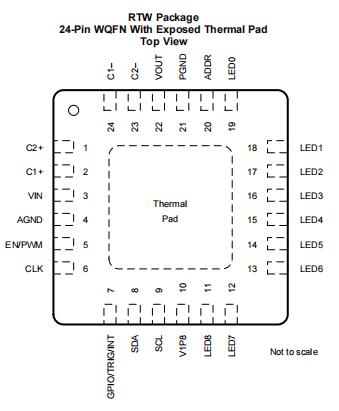
| PIN | TYPE | DESCRIPTION | |
| NAME | NO. | ||
| ADDR | 20 | I | I2C slave-address selection pin. |
| AGND | 4 | G | Analog and digital ground. Connect to PGND, exposed thermal pad, and common ground plane. |
| C1- | 24 | A | Negative pin of charge-pump flying capacitor 1. If a charge pump is not used, this pin must be left floating. |
| C1+ | 2 | A | Positive pin of charge-pump flying capacitor 1. If a charge pump is not used, this pin must be left floating. |
| C2- | 23 | A | Negative pin of charge-pump flying capacitor 2. If a charge pump is not used, this pin must be left floating. |
| C2+ | 1 | A | Positive pin of charge-pump flying capacitor 2. If a charge pump is not used, this pin must be left floating. |
| CLK | 6 | I, OD | Clock input/output. By default, this pin is a clock input. If not used, this pin must be connected to GND or VIN. |
| EN/PWM | 5 | I | Chip enable and PWM input pin. |
| GPIO/TRIG/INT | 7 | I, OD | General-purpose input or open-drain output, trigger input or open-drain output, or interrupt open-drain output. This pin function is configured in the I2C registers. By default, this pin is a general-purpose output (open-drain) and can be left floating if not used. |
| LED0 | 19 | A | LED current sink 0. If not used, this pin can be left floating. |
| LED1 | 18 | A | LED current sink 1. If not used, this pin can be left floating. |
| LED2 | 17 | A | LED current sink 2. If not used, this pin can be left floating. |
| LED3 | 16 | A | LED current sink 3. If not used, this pin can be left floating. |
| LED4 | 15 | A | LED current sink 4. If not used, this pin can be left floating. |
| LED5 | 14 | A | LED current sink 5. If not used, this pin can be left floating. |
| LED6 | 13 | A | LED current sink 6. If not used, this pin can be left floating. |
| LED7 | 12 | A | LED current sink 7. If not used, this pin can be left floating. |
| LED8 | 11 | A | LED current sink 8. If not used, this pin can be left floating. |
| PGND | 21 | G | Charge-pump power ground. Connect to AGND, exposed thermal pad, and common ground plane. |
| SCL | 9 | I | I2C bus clock line. If not used, this pin must be connected to GND or VIN. |
| SDA | 8 | I, OD | I2C bus data line. If not used, this pin must be connected to GND or VIN. |
| V1P8 | 10 | P | Input power for digital circuitry. |
| VIN | 3 | P | Input power, a 1-µF capacitor must be connected between PGND and this pin. |
| VOUT | 22 | A | Charge-pump output voltage. If a charge pump is used, a 1-µF capacitor must be connected between PGND and this pin. If charge pump is not used or is used in 1× the mode only, the capacitor can be omitted. |
LP5569RTWR Feature
Supply Voltage Range: 2.5 V–5.5 V • Nine High-Accuracy Current Sinks
– 25.5 mA Maximum per Channel
– 8-Bit Individual Current Control
– 12-Bit 20-kHz Internal Individual PWM Control Without Audio Noise
Three Programmable LED Engines
– Independent Illumination Control Without Active Microcontroller Control
– Synchronization Among Multiple Devices
– Up to 256 Instructions in SRAM Memory for Storing Sequences of Lighting Patterns
– LP5523 - and LP5523 1-Device-Compatible Command Set
Flexible Dimming Control
– I2C Dimming Control
– PWM Direct-Input Dimming
– PWM Input Frequency: 100-Hz to 20-kHz
Adaptive High-Efficiency Charge-Pump Control for driving High -VF LEDs With Low Battery Voltage
Master Fader Control Allows Dimming of MultipleLEDs by Writing to Only One Register to Reduce the I2C Bus Traffic
2-µA Low Standby Current and 10-µA in automatic Power-Save Mode When LEDs AreInactive
POR, UVLO, and TSD Protections
LP5569RTWR CAD Models
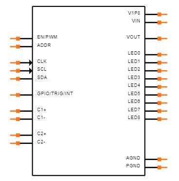
Symbol
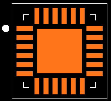
Footprint
3D Models
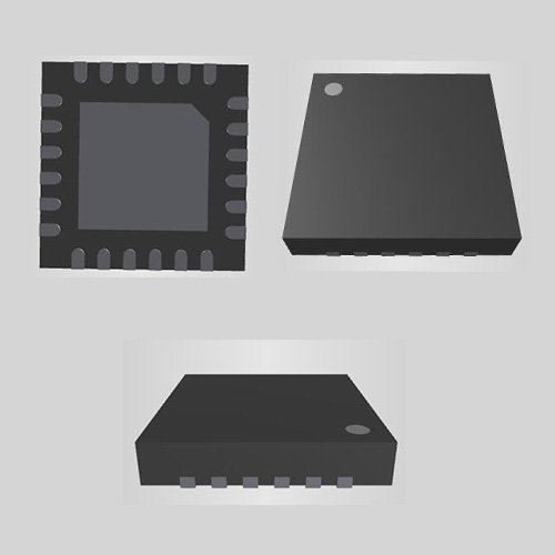
Specifications
- TypeParameter
- Lifecycle Status
Lifecycle Status refers to the current stage of an electronic component in its product life cycle, indicating whether it is active, obsolete, or transitioning between these states. An active status means the component is in production and available for purchase. An obsolete status indicates that the component is no longer being manufactured or supported, and manufacturers typically provide a limited time frame for support. Understanding the lifecycle status is crucial for design engineers to ensure continuity and reliability in their projects.
ACTIVE (Last Updated: 2 days ago) - Factory Lead Time6 Weeks
- Mounting Type
The "Mounting Type" in electronic components refers to the method used to attach or connect a component to a circuit board or other substrate, such as through-hole, surface-mount, or panel mount.
Surface Mount - Package / Case
refers to the protective housing that encases an electronic component, providing mechanical support, electrical connections, and thermal management.
24-WFQFN Exposed Pad - Surface Mount
having leads that are designed to be soldered on the side of a circuit board that the body of the component is mounted on.
YES - Number of Pins24
- SwitchingFrequency1.25MHz
- Operating Temperature
The operating temperature is the range of ambient temperature within which a power supply, or any other electrical equipment, operate in. This ranges from a minimum operating temperature, to a peak or maximum operating temperature, outside which, the power supply may fail.
-40°C~85°C - Packaging
Semiconductor package is a carrier / shell used to contain and cover one or more semiconductor components or integrated circuits. The material of the shell can be metal, plastic, glass or ceramic.
Tape & Reel (TR) - JESD-609 Code
The "JESD-609 Code" in electronic components refers to a standardized marking code that indicates the lead-free solder composition and finish of electronic components for compliance with environmental regulations.
e4 - Pbfree Code
The "Pbfree Code" parameter in electronic components refers to the code or marking used to indicate that the component is lead-free. Lead (Pb) is a toxic substance that has been widely used in electronic components for many years, but due to environmental concerns, there has been a shift towards lead-free alternatives. The Pbfree Code helps manufacturers and users easily identify components that do not contain lead, ensuring compliance with regulations and promoting environmentally friendly practices. It is important to pay attention to the Pbfree Code when selecting electronic components to ensure they meet the necessary requirements for lead-free applications.
yes - Part Status
Parts can have many statuses as they progress through the configuration, analysis, review, and approval stages.
Active - Moisture Sensitivity Level (MSL)
Moisture Sensitivity Level (MSL) is a standardized rating that indicates the susceptibility of electronic components, particularly semiconductors, to moisture-induced damage during storage and the soldering process, defining the allowable exposure time to ambient conditions before they require special handling or baking to prevent failures
2 (1 Year) - Number of Terminations24
- TypeLinear
- Terminal Finish
Terminal Finish refers to the surface treatment applied to the terminals or leads of electronic components to enhance their performance and longevity. It can improve solderability, corrosion resistance, and overall reliability of the connection in electronic assemblies. Common finishes include nickel, gold, and tin, each possessing distinct properties suitable for various applications. The choice of terminal finish can significantly impact the durability and effectiveness of electronic devices.
Nickel/Palladium/Gold (Ni/Pd/Au) - Applications
The parameter "Applications" in electronic components refers to the specific uses or functions for which a component is designed. It encompasses various fields such as consumer electronics, industrial automation, telecommunications, automotive, and medical devices. Understanding the applications helps in selecting the right components for a particular design based on performance, reliability, and compatibility requirements. This parameter also guides manufacturers in targeting their products to relevant markets and customer needs.
General Purpose - Terminal Position
In electronic components, the term "Terminal Position" refers to the physical location of the connection points on the component where external electrical connections can be made. These connection points, known as terminals, are typically used to attach wires, leads, or other components to the main body of the electronic component. The terminal position is important for ensuring proper connectivity and functionality of the component within a circuit. It is often specified in technical datasheets or component specifications to help designers and engineers understand how to properly integrate the component into their circuit designs.
QUAD - Number of Functions1
- Supply Voltage
Supply voltage refers to the electrical potential difference provided to an electronic component or circuit. It is crucial for the proper operation of devices, as it powers their functions and determines performance characteristics. The supply voltage must be within specified limits to ensure reliability and prevent damage to components. Different electronic devices have specific supply voltage requirements, which can vary widely depending on their design and intended application.
3.6V - Terminal Pitch
The center distance from one pole to the next.
0.5mm - Base Part Number
The "Base Part Number" (BPN) in electronic components serves a similar purpose to the "Base Product Number." It refers to the primary identifier for a component that captures the essential characteristics shared by a group of similar components. The BPN provides a fundamental way to reference a family or series of components without specifying all the variations and specific details.
LP5569 - Number of Outputs9
- Output Voltage
Output voltage is a crucial parameter in electronic components that refers to the voltage level produced by the component as a result of its operation. It represents the electrical potential difference between the output terminal of the component and a reference point, typically ground. The output voltage is a key factor in determining the performance and functionality of the component, as it dictates the level of voltage that will be delivered to the connected circuit or load. It is often specified in datasheets and technical specifications to ensure compatibility and proper functioning within a given system.
5.5V - Max Supply Voltage
In general, the absolute maximum common-mode voltage is VEE-0.3V and VCC+0.3V, but for products without a protection element at the VCC side, voltages up to the absolute maximum rated supply voltage (i.e. VEE+36V) can be supplied, regardless of supply voltage.
5.5V - Min Supply Voltage
The minimum supply voltage (V min ) is explored for sequential logic circuits by statistically simulating the impact of within-die process variations and gate-dielectric soft breakdown on data retention and hold time.
2.5V - Output Current
The rated output current is the maximum load current that a power supply can provide at a specified ambient temperature. A power supply can never provide more current that it's rated output current unless there is a fault, such as short circuit at the load.
160mA - Topology
In the context of electronic components, "topology" refers to the arrangement or configuration of the components within a circuit or system. It defines how the components are connected to each other and how signals flow between them. The choice of topology can significantly impact the performance, efficiency, and functionality of the electronic system. Common topologies include series, parallel, star, mesh, and hybrid configurations, each with its own advantages and limitations. Designers carefully select the appropriate topology based on the specific requirements of the circuit to achieve the desired performance and functionality.
Switched Capacitor (Charge Pump) - Internal Switch(s)
The term "Internal Switch(s)" in electronic components typically refers to a built-in mechanism within a device that allows for the control of electrical current flow. These internal switches can be used to turn circuits on or off, change the direction of current, or regulate the flow of electricity within the component. They are often designed to be controlled externally, either manually or automatically, to enable various functions or operations within the electronic device. Internal switches play a crucial role in the overall functionality and performance of electronic components by providing a means to manage and manipulate electrical signals effectively.
No - fmax-Min
fmax-Min refers to the frequency range that an electronic component or system can operate within. It represents the difference between the maximum frequency (fmax) and the minimum frequency (Min) limits of operation. This parameter is crucial in defining the bandwidth of the component, indicating how effectively it can transmit or receive signals over that range. A wider fmax-Min value typically signifies better performance for applications that require broad frequency response.
0.4 MHz - Dimming
Dimming is a feature in electronic components, such as LED lights or display screens, that allows the user to adjust the brightness level of the device. It is a method of controlling the amount of light output by the component, typically by varying the voltage or current supplied to it. Dimming can be achieved through various techniques, such as pulse-width modulation (PWM) or analog dimming. This feature is commonly used to save energy, create ambiance, or enhance visual comfort in different applications.
I2C, PWM - Number of Segments9
- Max Junction Temperature (Tj)
Max Junction Temperature (Tj) refers to the maximum allowable temperature at the junction of a semiconductor device, such as a transistor or integrated circuit. It is a critical parameter that influences the performance, reliability, and lifespan of the component. Exceeding this temperature can lead to thermal runaway, breakdown, or permanent damage to the device. Proper thermal management is essential to ensure the junction temperature remains within safe operating limits during device operation.
125°C - Voltage - Supply (Min)
Voltage - Supply (Min) is a parameter in electronic components that specifies the minimum voltage required for the component to operate within its specified performance range. This parameter indicates the lowest voltage level that can be safely applied to the component without causing malfunctions or damage. It is crucial to ensure that the supply voltage provided to the component is equal to or higher than the specified minimum voltage to guarantee proper functionality and reliability. Failure to meet this requirement may result in erratic behavior, reduced performance, or even permanent damage to the component.
2.5V - Multiplexed Display Capability
Multiplexed Display Capability refers to the ability of an electronic component or system to control multiple display elements using fewer input/output lines. This is achieved by rapidly switching between different displays or segments, allowing for efficient communication and reduced wiring complexity. In multiplexed systems, each display is activated sequentially, creating the illusion of simultaneous display to the user. This capability is commonly utilized in devices like LED matrices and LCD screens to enhance functionality while conserving space and resources.
NO - Ambient Temperature Range High
This varies from person to person, but it is somewhere between 68 and 77 degrees F on average. The temperature setting that is comfortable for an individual may fluctuate with humidity and outside temperature as well. The temperature of an air conditioned room can also be considered ambient temperature.
85°C - Data Input Mode
Data Input Mode in electronic components refers to the specific method or protocol used to input data into the component. This parameter determines how data is received and processed by the component, whether it be through serial communication, parallel communication, or other interfaces. The data input mode is crucial for ensuring compatibility and proper functioning of the component within a larger electronic system. Understanding and configuring the data input mode correctly is essential for effective data transfer and communication between different components in a circuit or system.
SERIAL - Height800μm
- Length4mm
- Width4mm
- Thickness
Thickness in electronic components refers to the measurement of how thick a particular material or layer is within the component structure. It can pertain to various aspects, such as the thickness of a substrate, a dielectric layer, or conductive traces. This parameter is crucial as it impacts the electrical, mechanical, and thermal properties of the component, influencing its performance and reliability in electronic circuits.
750μm - RoHS Status
RoHS means “Restriction of Certain Hazardous Substances” in the “Hazardous Substances Directive” in electrical and electronic equipment.
ROHS3 Compliant
LP5569RTWR Applications
LED Lighting, Indicator Lights, and Fun Lights for:
• Smart Speaker
• Smart Home Appliance
• Doorbell
• Electric Lock
• Smoke Detector
• Thermostat
• Set-Top Box
• Smart Router
• Bluetooth® Headset
• Cell Phone
LP5569RTWR Applications Circuit
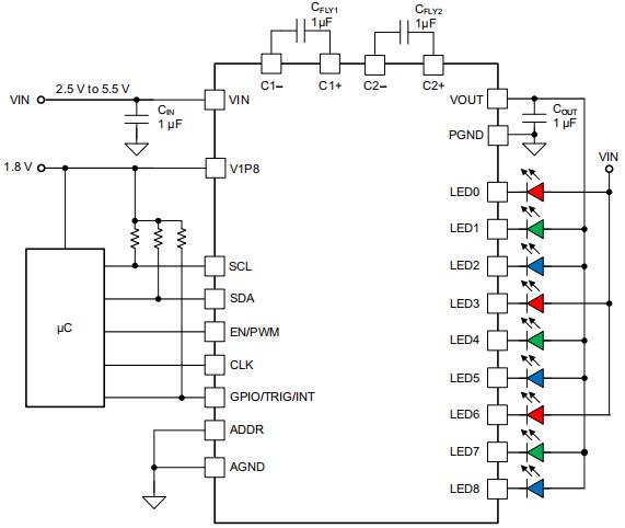
LP5569RTWR Functional Block Diagram
LP5569RTWR Manufacturer
Texas Instruments Incorporated (TI) is an American technology company based in Dallas, Texas, that designs and manufactures semiconductors and integrated circuits for electronic designers and manufacturers around the world. Based on sales volume, it is one of the top ten semiconductor companies in the world. Analog chips and embedded processors, which account for more than 80 % of the company's revenue, are the company's main focus. TI also makes calculators, microcontrollers, and multi-core processors, as well as TI digital light processing technology and education technology, As of 2016, the company had 45,000 patents worldwide.
LP5569RTWR Package
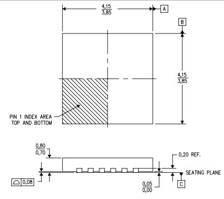
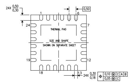
LP5569RTWR Advantages
Current Sinks
The LP5569RTWR LED drivers are constant-current sources. Maximum output-current scale can be programmed by control registers up to 25.5 mA.
Charge Pump
The LP5569RTWR device includes a pre-regulated switched-capacitor charge pump with a programmable voltage multiplication of 1× or 1.5×.
Energy Efficiency
The red LED (R) element of an RGB LED typically has a forward voltage of about 2 V. these LED s can be powered directly from the input voltage because battery voltage is typically high enough to drive red LED s over the whole operating voltage range.
Automatic Power-Save Mode
When the LED outputs are not active, the LP5569RTWR device is able to enter power-save mode automatically, thus lowering idle-current consumption down to TBD μA (typical). Automatic power-save mode is enabled when the MISC register (address 2Fh) POWERSAVE_EN bit = 1.
Protection Features
It has four protection features, including Thermal Shutdown, Undervoltage Lockout (UVLO), Power-On Reset (POR), LED Fault Detection
Clock Generation and Synchronization
The LP5569RTWR device can generate a 32-kHz clock signal and use it for synchronizing multiple devices. The CLK pin is configured as an input by default
P5569RTWR Dimensions
| Height | 800μm |
| Length | 4mm |
| Thickness | 750μm |
| Width | 4mm |
Trend Analysis
Datasheet PDF
- Datasheets :
Parts with Similar Specs
What is LP5569RTWR?
The LP5569RTWR device is a fully integrated lighting management unit for producing lighting effects for various LED applications. The LP5569RTWR device includes all necessary power management, low-side current sinks, a two-wire serial I2C-compatible interface, and programmable LED engines.
Does LP5569RTWR have protection features?
Yes, its protection features include power-on reset, charge-pump, input-current limiter, thermal shutdown(TSD), and under-voltage lockout(UVLO).
Can LP5569RTWR be operated in 100℃?
No, its operating temperature is between -40 and 85℃.
Where is LP5569RTWR made from?
It is made by an American company-Texas Instruments Incorporated.
What’s the main parameters of LP5569RTWR?
the main parameters of this part are: Nine-channel I2C RGB LED driver with engine control and charge pump 24-WQFN -40 to 85.
 STM8AF6223PDU Microcontroller: Technical Overview
29 February 2024176
 ATtiny4313 Microcontroller: Pinout, Datasheet, Block Diagram
26 October 20211824
![A General Introduction to BMX055 [Faq]](https://res.utmel.com/Images/Article/d62f1040-06a8-4a63-aaf9-208b94cf45a1.jpg) A General Introduction to BMX055 [Faq]
A General Introduction to BMX055 [Faq]20 April 20221839
![2N3053 BJT Transistor: Datasheet, Pinout, Circuit [FAQ&Video]](https://res.utmel.com/Images/Article/73b60587-50f2-45df-b152-447f4f044b9f.jpg) 2N3053 BJT Transistor: Datasheet, Pinout, Circuit [FAQ&Video]
2N3053 BJT Transistor: Datasheet, Pinout, Circuit [FAQ&Video]04 May 20224139
 ATxmega64A1U and ATxmega128A1U Microcontrollers: Technical Overview and Specifications
29 February 2024264
 M93C66-W 4-Kbit MICROWIRE™ Serial EEPROM: Pinout, Equivalent and Datasheet
08 March 20221304
 Best Alternatives to Murata GCJ188R72A104KA01D Capacitor
21 August 20252064
 STM32H747XIH6 Microcontroller: Features, Applications and Datasheet
26 December 20237431
 Analysis of Common Misunderstandings of Isolation Technology
25 April 20225994
 Role of Direct Memory Access in Modern Computing
12 November 20246171
 Exploring SPI Communication for Faster Data Transfer
20 June 20251465
 Linear Induction Motor: Working Principle, Characteristics, and Applications
02 March 202115674
 H-bridge: Working, Circuits and Applications
03 December 202146316
 Understanding the Basics of I2C Interface Controllers
11 June 20251734
 What is a Servo Drive?
16 June 20215751
 Commonly Used Sensitive Resistor Type Foundation and Circuit Application
16 December 20213598
Texas Instruments
In Stock: 10000
United States
China
Canada
Japan
Russia
Germany
United Kingdom
Singapore
Italy
Hong Kong(China)
Taiwan(China)
France
Korea
Mexico
Netherlands
Malaysia
Austria
Spain
Switzerland
Poland
Thailand
Vietnam
India
United Arab Emirates
Afghanistan
Åland Islands
Albania
Algeria
American Samoa
Andorra
Angola
Anguilla
Antigua & Barbuda
Argentina
Armenia
Aruba
Australia
Azerbaijan
Bahamas
Bahrain
Bangladesh
Barbados
Belarus
Belgium
Belize
Benin
Bermuda
Bhutan
Bolivia
Bonaire, Sint Eustatius and Saba
Bosnia & Herzegovina
Botswana
Brazil
British Indian Ocean Territory
British Virgin Islands
Brunei
Bulgaria
Burkina Faso
Burundi
Cabo Verde
Cambodia
Cameroon
Cayman Islands
Central African Republic
Chad
Chile
Christmas Island
Cocos (Keeling) Islands
Colombia
Comoros
Congo
Congo (DRC)
Cook Islands
Costa Rica
Côte d’Ivoire
Croatia
Cuba
Curaçao
Cyprus
Czechia
Denmark
Djibouti
Dominica
Dominican Republic
Ecuador
Egypt
El Salvador
Equatorial Guinea
Eritrea
Estonia
Eswatini
Ethiopia
Falkland Islands
Faroe Islands
Fiji
Finland
French Guiana
French Polynesia
Gabon
Gambia
Georgia
Ghana
Gibraltar
Greece
Greenland
Grenada
Guadeloupe
Guam
Guatemala
Guernsey
Guinea
Guinea-Bissau
Guyana
Haiti
Honduras
Hungary
Iceland
Indonesia
Iran
Iraq
Ireland
Isle of Man
Israel
Jamaica
Jersey
Jordan
Kazakhstan
Kenya
Kiribati
Kosovo
Kuwait
Kyrgyzstan
Laos
Latvia
Lebanon
Lesotho
Liberia
Libya
Liechtenstein
Lithuania
Luxembourg
Macao(China)
Madagascar
Malawi
Maldives
Mali
Malta
Marshall Islands
Martinique
Mauritania
Mauritius
Mayotte
Micronesia
Moldova
Monaco
Mongolia
Montenegro
Montserrat
Morocco
Mozambique
Myanmar
Namibia
Nauru
Nepal
New Caledonia
New Zealand
Nicaragua
Niger
Nigeria
Niue
Norfolk Island
North Korea
North Macedonia
Northern Mariana Islands
Norway
Oman
Pakistan
Palau
Palestinian Authority
Panama
Papua New Guinea
Paraguay
Peru
Philippines
Pitcairn Islands
Portugal
Puerto Rico
Qatar
Réunion
Romania
Rwanda
Samoa
San Marino
São Tomé & Príncipe
Saudi Arabia
Senegal
Serbia
Seychelles
Sierra Leone
Sint Maarten
Slovakia
Slovenia
Solomon Islands
Somalia
South Africa
South Sudan
Sri Lanka
St Helena, Ascension, Tristan da Cunha
St. Barthélemy
St. Kitts & Nevis
St. Lucia
St. Martin
St. Pierre & Miquelon
St. Vincent & Grenadines
Sudan
Suriname
Svalbard & Jan Mayen
Sweden
Syria
Tajikistan
Tanzania
Timor-Leste
Togo
Tokelau
Tonga
Trinidad & Tobago
Tunisia
Turkey
Turkmenistan
Turks & Caicos Islands
Tuvalu
U.S. Outlying Islands
U.S. Virgin Islands
Uganda
Ukraine
Uruguay
Uzbekistan
Vanuatu
Vatican City
Venezuela
Wallis & Futuna
Yemen
Zambia
Zimbabwe
![UCC25710DWR]() UCC25710DWR
UCC25710DWRTexas Instruments
![LM3447MTX/NOPB]() LM3447MTX/NOPB
LM3447MTX/NOPBTexas Instruments
![TPS61040DBVR]() TPS61040DBVR
TPS61040DBVRTexas Instruments
![TPS61041DBVR]() TPS61041DBVR
TPS61041DBVRTexas Instruments
![TPS61165DRVR]() TPS61165DRVR
TPS61165DRVRTexas Instruments
![LM3409HVMY/NOPB]() LM3409HVMY/NOPB
LM3409HVMY/NOPBTexas Instruments
![TLC59116IRHBR]() TLC59116IRHBR
TLC59116IRHBRTexas Instruments
![TLC5971PWPR]() TLC5971PWPR
TLC5971PWPRTexas Instruments
![TLC5940PWPR]() TLC5940PWPR
TLC5940PWPRTexas Instruments
![TLC5922DAP]() TLC5922DAP
TLC5922DAPTexas Instruments


