
 Product
 Brand
Brand Articles
 Tools
Tools
AD9528 Clock Generator Integration Notes: Solving PLL Unlocking and Phase Noise

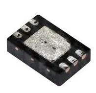
3.3V AD9528 Clock Generators 72 Pins 72-VFQFN Exposed Pad, CSP 72 Terminals Surface Mount 3.135V~3.465V Cut Tape (CT)
Unit Price: $10.334849
Ext Price: $10.33


3.3V AD9528 Clock Generators 72 Pins 72-VFQFN Exposed Pad, CSP 72 Terminals Surface Mount 3.135V~3.465V Cut Tape (CT)
Discover design and integration notes for the AD9528 dual-PLL clock generator. Learn how to optimize phase noise, fix PLL1 unlocking, and compare alternatives.
- Critical Electrical Specifications and System Impact
- Overcoming PLL1 Unlocking and Initialization Failures
- Optimizing Phase Noise Performance at Low Offsets
- Software Configuration: Escaping the Device Tree Nightmare
- Application Contexts
- Competitors, Alternatives, and Replacement Strategy
- Datasheet, Pinout, and Layout Verification
- Frequently Asked Questions
- Specifications
- Parts with Similar Specs
- Datasheet PDF
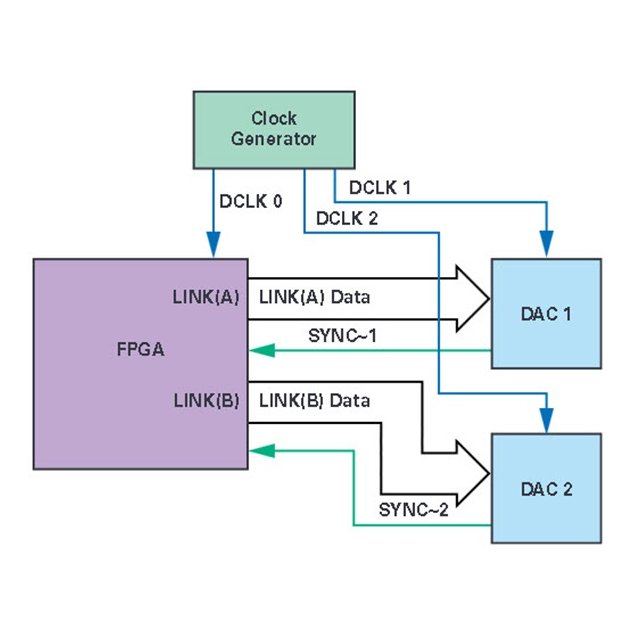
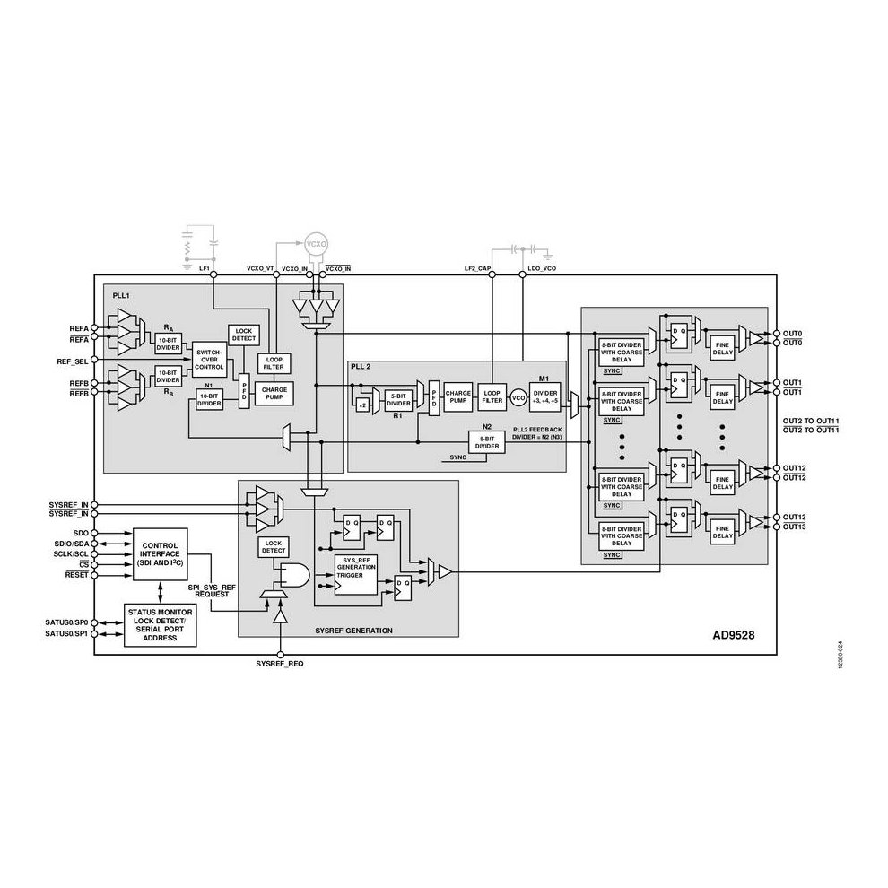
The AD9528 is a two-stage phase-locked loop (PLL) with an integrated JESD204B/JESD204C SYSREF generator designed for multiple device synchronization and clock jitter reduction. Primarily utilized in high-speed data acquisition and cellular infrastructure, this component acts as the timing heartbeat for complex arrays of ADCs, DACs, and transceivers where deterministic latency and ultra-low phase noise are non-negotiable.
When evaluating this clock generator for a new bill of materials (BOM) or debugging an existing prototype, engineers must look beyond the top-line jitter specs. The realities of integrating a dual-loop architecture involve strict power sequencing, precise register configurations, and careful loop filter design.
Core Architecture: Dual PLL (PLL1 for jitter cleaning/reference selection, PLL2 for high-frequency VCO generation).
Output Flexibility: 14 independent outputs, software-configurable for HSTL or LVDS signaling.
Primary Application: Clocking high-speed data converters (ADCs, DACs, DDSs) requiring JESD204B/C SYSREF alignment.
Key Integration Challenge: Manually calculating register values for the two-stage PLL and SYSREF dividers is highly error-prone without vendor software.
Critical Electrical Specifications and System Impact
Clock generators are evaluated on their ability to maintain signal integrity across multiple distribution paths without introducing timing errors that would degrade a data converter's Signal-to-Noise Ratio (SNR).
VCO Tuning Range (3.6 GHz to 4.0 GHz): The internal voltage-controlled oscillator operates in this high-frequency band. The specific tuning range dictates the allowable integer and fractional divider ratios used to hit your target output frequencies. Operating near the edges of this range requires careful attention to the PLL2 loop filter design to maintain lock over temperature variations.
Absolute Output Jitter (<160 fs at 122.88 MHz): In high-performance wireless transceivers, jitter translates directly to phase noise, which degrades the Error Vector Magnitude (EVM) of transmitted signals and the sensitivity of receivers. Sub-160 femtosecond performance places this device firmly in the "carrier-grade" category.
Typical Output-to-Output Skew (20 ps): When synchronizing multiple JESD204B converters, the SYSREF and device clocks must arrive at all endpoints with tightly controlled phase alignment to achieve deterministic latency. A 20 ps skew across 14 outputs provides generous timing margin for PCB trace length mismatch.
14 Configurable Outputs: The ability to toggle individual outputs between HSTL and LVDS allows mixed-signal boards to drive different logic families without requiring external level translators, saving significant board space and BOM cost.
Overcoming PLL1 Unlocking and Initialization Failures
One of the most common hurdles engineers face during board bring-up with the AD9528 is PLL1 failing to lock to the reference clock, or unexpectedly dropping lock with the onboard VCXO. Because the dual-PLL architecture relies on PLL1 to clean the noisy system reference before feeding it to PLL2, a failure here cascades through the entire timing tree.
If you are experiencing unexpected unlocking, the root cause is rarely a defective chip; it is almost always power delivery or initialization sequencing.
First, probe the LDO_VCO voltage. The internal VCO requires a highly stable 2.5V supply to operate correctly. If the external supply network is drooping under dynamic load, or if the internal LDO is improperly bypassed, the VCO will drift out of the tuning band, causing a lock failure.
Secondly, verify the SPI register initialization sequence. The digital frequency lock detect circuitry is highly sensitive to the order in which registers are written. If the reference clock inputs are not stable before the PLL1 dividers are engaged, the state machine can hang. Always ensure the reference clocks are actively toggling before asserting the final software reset and calibration commands over the SPI/I2C port.
Optimizing Phase Noise Performance at Low Offsets
While the broadband jitter of this component is excellent, meeting aggressive phase noise targets at low frequency offsets (e.g., 100 Hz) requires manual intervention in the loop dynamics. Users often find that the default evaluation board settings do not provide the necessary low-frequency noise rejection for sensitive medical instrumentation (like MRI or ultrasound receivers) or multicarrier GSM base stations.
To fix this, you must manipulate the trade-off between PLL1 and PLL2. 1. Reduce the PLL1 loop bandwidth: A narrower loop bandwidth on the first stage forces the system to rely more heavily on the clean, external VCXO for close-in phase noise rather than the noisy upstream system reference. 2. Increase the PLL2 charge pump current: Driving the internal VCO with a higher charge pump current improves the phase noise profile of the second stage, though it will require recalculating the external loop filter components (resistors and capacitors) to maintain phase margin and stability.
Software Configuration: Escaping the Device Tree Nightmare
Because this device features a two-stage PLL, duty cycle correction for odd divider settings, and an integrated JESD204B/C SYSREF generator, the internal register map is vast. Calculating the correct clock rates, divider ratios, and SYSREF delays manually to write into a Linux device tree or bare-metal C code is exceptionally difficult and a primary source of integration delays.
Do not attempt to calculate these registers by hand. The standard engineering practice is to use the manufacturer's evaluation software (ADIsimCLK). This tool allows you to visually construct the timing tree, input your target phase noise requirements, and automatically generate the correct register hex dumps. You can then export these configurations directly into your microcontroller's initialization routines, bypassing the complex math required for dual-loop frequency planning.
Application Contexts
The component's architecture dictates its use in environments where multiple high-speed devices must act in perfect unison.
Wireless Infrastructure (LTE/GSM Base Stations): The dual-loop architecture is purpose-built to take a jittery backplane reference (like a recovered SyncE clock), clean it with a high-Q VCXO via PLL1, and distribute pristine LO reference clocks to RF transceivers.
Medical Instrumentation (Ultrasound and MRI): Phased-array systems require dozens of ADCs to sample returning signals simultaneously. The 14 outputs and 20 ps skew ensure that the beamforming algorithms are not corrupted by timing mismatch between channels.
ATE and High-Performance Instrumentation: Automated test equipment relies on the digital frequency lock detect and duty cycle correction to provide reliable, variable-frequency test vectors to devices under test (DUTs) without introducing measurement artifacts.
Competitors, Alternatives, and Replacement Strategy
When dealing with supply chain constraints or evaluating second-source options, the clock generator market is highly specialized. There are no true "drop-in" replacements for complex JESD204B clockers, as every manufacturer utilizes different register maps, pinouts, and loop filter architectures.
If you are looking at alternatives to the AD9528, the primary competitors include:
Texas Instruments LMK04828: This is the most direct functional rival. It also features a dual-PLL architecture and JESD204B SYSREF generation. However, the LMK04828 has a completely different SPI register structure and footprint. Moving from Analog Devices to TI will require a full PCB respin and a complete rewrite of the initialization firmware.
Silicon Labs Si5345: Silicon Labs utilizes a DSPLL architecture rather than a traditional analog dual-PLL. This often results in a smaller external component footprint (fewer external loop filter capacitors), but the phase noise profile behaves differently, particularly at low offsets.
Renesas 8V97003 & Silicon Labs Si53306: These are often evaluated in similar BOMs, though they may serve slightly different roles depending on whether the primary goal is sheer fanout (Si53306) or wideband RF generation.
Procurement Note: Because migrating between these parts requires immense software and hardware qualification effort, procurement teams should secure long-term pipeline visibility for their chosen clock generator early in the design phase.
Datasheet, Pinout, and Layout Verification
Before finalizing your schematic capture and PCB layout, several critical physical parameters must be verified against the manufacturer's documentation.
Thermal Pad Grounding: The exposed paddle on the bottom of the package is not just for thermal dissipation; it is the primary electrical ground for the internal RF circuitry. It must be soldered to a continuous ground plane using a dense matrix of thermal vias. Failure to do so will result in degraded phase noise and erratic VCO behavior. Exact thermal derating will depend heavily on your PCB copper area, so checking the manufacturer's specific layout guidelines is strictly required here.
Power Supply Decoupling: The device features multiple power domains (VCO, charge pump, digital, and output drivers). Do not tie all VDD pins to a single rail without proper LC filtering. The outputs will easily couple switching noise back into the sensitive VCO supply if the decoupling network is inadequate.
Loop Filter Proximity: The passive components for both PLL1 and PLL2 loop filters must be placed as close to the designated pins as physically possible to prevent EMI injection into the high-impedance charge pump nodes.
Frequently Asked Questions
Why does the AD9528 fail to lock on the onboard VCXO during cold boot?This is typically caused by either a voltage drop on the internal LDO_VCO (which must be strictly maintained at 2.5V) or an incorrect SPI initialization sequence where the dividers are engaged before the reference clock has stabilized.
How can I improve the phase noise performance at 100 Hz offset?You must adjust the trade-off between the two PLL stages. Use ADIsimCLK to reduce the loop bandwidth of PLL1 (relying more on the clean VCXO) and simultaneously increase the charge pump current of PLL2.
Can I replace the AD9528 with the TI LMK04828 without changing my PCB?No. While they serve the exact same functional role in a JESD204B system (dual-PLL jitter cleaning and SYSREF generation), they have different pinouts, different loop filter requirements, and entirely different software register maps. A hardware respin and firmware rewrite are mandatory.
Do I have to write the device tree configuration manually for Linux integration?It is highly discouraged. Calculating the correct odd-divider duty cycle corrections and SYSREF timing manually is prone to severe errors. Use the AD9528 Evaluation Software (ADIsimCLK) to generate the required register configurations and export them to your driver.
Specifications
Parts with Similar Specs
- ImagePart NumberManufacturerPackage / CaseNumber of PinsPLLInputFrequency (Max)Supply VoltageRoHS StatusFactory Lead TimeView Compare
![AD9528BCPZ-REEL7]()
AD9528BCPZ-REEL7
72-VFQFN Exposed Pad, CSP
72
Yes with Bypass
CMOS, HSTL, LVDS
1.25GHz
3.3 V
ROHS3 Compliant
8 Weeks
![AD9520-3BCPZ]()
64-VFQFN Exposed Pad, CSP
64
Yes
CMOS, LVDS, LVPECL
-
3.3 V
ROHS3 Compliant
8 Weeks
![AD9516-5BCPZ]()
64-VFQFN Exposed Pad, CSP
64
Yes
CMOS, LVDS, LVPECL
2.4GHz
3.3 V
ROHS3 Compliant
8 Weeks
![AD9516-5BCPZ-REEL7]()
64-VFQFN Exposed Pad, CSP
64
Yes
CMOS, LVDS, LVPECL
2.4GHz
-
ROHS3 Compliant
8 Weeks


Datasheet PDF
- Datasheets :
- Other Related Documents :
- PCN Design/Specification :
- ConflictMineralStatement :
 AD7291 ADC Design Notes: Resolving I2C Arbitration, Temperature Stability, and Driver Bugs
06 May 2026138
![IRF640N MOSFET Transistor[FAQ+Video]: Datasheet, Equivalent, and Pinout](https://res.utmel.com/Images/Article/9e89980f-2517-420e-a3f3-33df0721c298.jpg) IRF640N MOSFET Transistor[FAQ+Video]: Datasheet, Equivalent, and Pinout
IRF640N MOSFET Transistor[FAQ+Video]: Datasheet, Equivalent, and Pinout11 April 202210096
 MAX30102 Sensor: Datasheet, Pinout and Schematic
09 August 202119437
 Designing Ultra-Compact Electronics with ATTINY10: Specs, Pinout, and TPI Programming
06 February 2026211
 LR43 Battery, 1.5 V Alkaline Button Cell Battery and LR43 Equivalents
23 February 202210533
 BC640 PNP Silicon Transistor: BC640, Datasheet, Equivalent
07 January 202210517
 LD39050PU33R: 5.5V, 6-VDFN Exposed Pad, Pinout and Datasheet
02 March 20222041
![ATTINY45-20PU AVR series Microcontroller IC 8-Bit 20MHz[FAQ]: Datasheet, Features, and Pinout](https://res.utmel.com/Images/Article/a56c3c5f-b7ab-4a23-b644-a7088ffc38d8.jpg) ATTINY45-20PU AVR series Microcontroller IC 8-Bit 20MHz[FAQ]: Datasheet, Features, and Pinout
ATTINY45-20PU AVR series Microcontroller IC 8-Bit 20MHz[FAQ]: Datasheet, Features, and Pinout18 March 20221309
 Amorphous Silicon Solar Cells: Features, Structure and Applications
22 August 20226499
 An Overview of Digital Signal Processor
31 October 202510861
 Introduction to TTL and CMOS Logic Gate Circuits
24 November 202522512
 All You Need to Know About Rectifier Circuit
24 April 202517468
 Working Principle and Characteristics of Zener diodes
20 October 202525280
 Why Meta Did Not Choose Qualcomm AI Chip?
02 April 20225972
 Will Sodium-ion Battery be the Next Gen of Battery?
29 September 20214494
 Understanding Machine Vision and Visual Sensor
27 September 20212157
Analog Devices Inc.
In Stock: 5840
Minimum: 1 Multiples: 1
Qty
Unit Price
Ext Price
1
$10.334849
$10.33
10
$9.749858
$97.50
100
$9.197979
$919.80
500
$8.677339
$4,338.67
1000
$8.186168
$8,186.17
Not the price you want? Send RFQ Now and we'll contact you ASAP.
Inquire for More Quantity
![ADF4118BRU-REEL7]() ADF4118BRU-REEL7
ADF4118BRU-REEL7Analog Devices Inc.
![AD9522-3BCPZ]() AD9522-3BCPZ
AD9522-3BCPZAnalog Devices Inc.
![AD9518-4ABCPZ]() AD9518-4ABCPZ
AD9518-4ABCPZAnalog Devices Inc.
![AD9517-3ABCPZ]() AD9517-3ABCPZ
AD9517-3ABCPZAnalog Devices Inc.
![AD9520-0BCPZ]() AD9520-0BCPZ
AD9520-0BCPZAnalog Devices Inc.
![AD9542BCPZ-REEL7]() AD9542BCPZ-REEL7
AD9542BCPZ-REEL7Analog Devices Inc.
![AD9574BCPZ]() AD9574BCPZ
AD9574BCPZAnalog Devices Inc.
![ADF4110BCPZ]() ADF4110BCPZ
ADF4110BCPZAnalog Devices Inc.
![ADF4113HVBRUZ]() ADF4113HVBRUZ
ADF4113HVBRUZAnalog Devices Inc.
![ADF4150HVBCPZ]() ADF4150HVBCPZ
ADF4150HVBCPZAnalog Devices Inc.


