

 Product
 Brand
Brand Articles
 Tools
Tools
AD9144 DAC Integration Notes: JESD204B Synchronization, Blanking Instability, and Replacements


DPG3 EVALUATION BOARD WITH ADRF6720 MODULATOR
Evaluate the AD9144 quad 16-bit DAC for multicarrier systems. Review critical JESD204B sync troubleshooting, thermal margins, and TI DAC37J84 alternatives.
- Key Electrical Specifications and System Trade-offs
- Overcoming JESD204B Sync Issues in Subclass 1 Mode
- Diagnosing Blanking State Machine Instability
- Thermal Sensitivity During Sync Processing
- Application Mapping: Base Stations, SDRs, and MIMO
- Evaluating AD9144 Alternatives and Equivalents
- Datasheet and Layout Verification Steps
- Hyper-Specific FAQ
- Specifications
- Parts with Similar Specs
- Datasheet PDF
The AD9144 is a quad, 16-bit, high dynamic range digital-to-analog converter (DAC) designed for multicarrier generation up to the Nyquist frequency. Because it supports a maximum sample rate of 2.8 GSPS and utilizes a flexible 8-lane JESD204B interface, it is heavily adopted in complex RF transmit chains where multiple wideband signals must be synthesized synchronously.
While its core specifications make it highly capable for advanced digital-to-RF architectures, integrating a quad-channel, multi-GSPS converter introduces strict requirements for high-speed serial link stability, thermal management, and state-machine initialization.
Resolution: 16-bit
Maximum Sample Rate: 2.8 GSPS
Digital Interface: Flexible 8-lane JESD204B
Power Consumption: 1.6 W at 1.6 GSPS
Full-Scale Output Current: 13.9 mA to 27.0 mA
Interpolation Options: Selectable 1x, 2x, 4x, 8x
Key Electrical Specifications and System Trade-offs
Selecting the AD9144 requires balancing its high-speed capabilities against the realities of power distribution and signal integrity. The device delivers an impressive 2.8 GSPS maximum sample rate per channel, which provides massive bandwidth for multicarrier generation. However, pushing four channels at these speeds demands significant data throughput from the host FPGA or ASIC, necessitating the 8-lane JESD204B interface.
The integration trade-off here is PCB complexity versus physical footprint. While the serial JESD204B interface drastically reduces the pin count compared to parallel LVDS interfaces, it requires tightly controlled 100-ohm differential routing, strict length matching across lanes, and robust equalization.
Power consumption is rated at 1.6 W at 1.6 GSPS. Operating at the maximum 2.8 GSPS with all four channels and higher interpolation rates engaged will push the power dissipation higher. This thermal load must be actively managed, as temperature fluctuations directly impact the timing margins of the high-speed serial link. The full-scale output current is tunable between 13.9 mA and 27.0 mA, allowing engineers to optimize the dynamic range and compliance voltage for the specific downstream RF amplifier or modulator being driven.
Overcoming JESD204B Sync Issues in Subclass 1 Mode
The most complex aspect of integrating the AD9144 is establishing and maintaining a stable JESD204B link, particularly when deterministic latency is required across multiple chips.
A frequent and critical pain point during board bring-up is the SYNC_BUSY signal remaining stuck at '1'. In subclass 1 mode, this indicates that the DAC is failing to achieve Code Group Synchronization (CGS) or is unable to lock to the sync signal. Furthermore, engineers often observe variable delays from the SYSREF signal to the SYNC signal across different power cycles.
To resolve these synchronization failures, focus your debugging on the following areas:
Dual DAC Pair Configuration: The AD9144 internally manages its four channels as two distinct DAC pairs. Ensure that both pairs are properly configured in your SPI register writes. A misconfiguration in one pair can hold the entire link in a busy state.
HDL Instantiation Parameters: Verify that the JESD204B IP core in the host FPGA is configured with the exact matching parameters (L, M, F, S, K) expected by the AD9144. A mismatch in the number of frames per multiframe (K) is a common culprit for sync lock failures.
Clock and SYSREF Distribution: Variable delays across power cycles almost always point to setup and hold time violations on the SYSREF signal relative to the device clock. The SYSREF signal must be captured synchronously by the device clock at both the FPGA and the AD9144. Use a low-jitter clock distribution IC to guarantee that the phase relationship between the device clock and SYSREF remains deterministic.
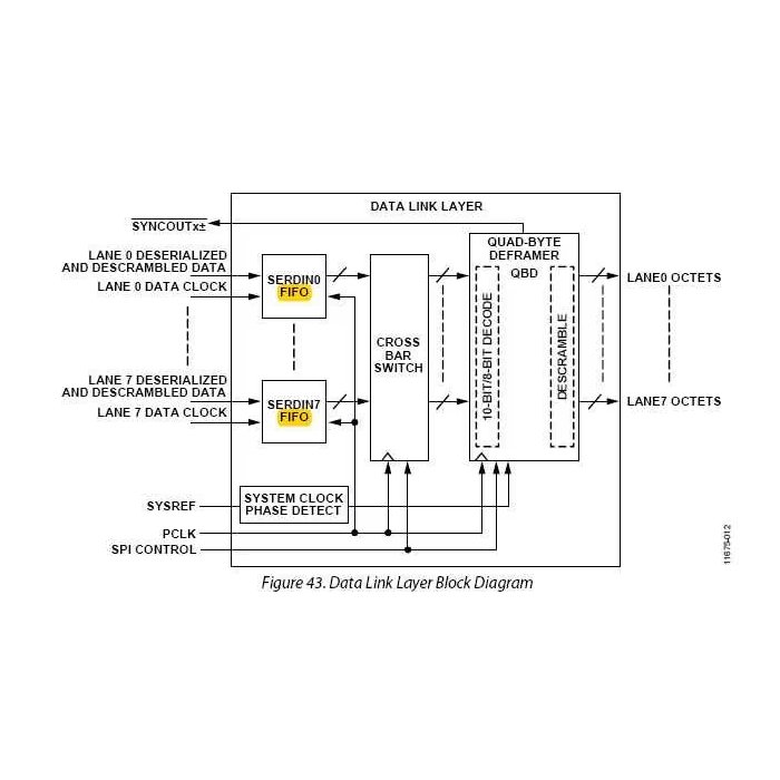
Diagnosing Blanking State Machine Instability
Another severe integration hurdle occurs when the system randomly boots into a blanking state, resulting in a complete loss of the RF output signal. The AD9144 includes a protective state machine designed to mute the DAC outputs (soft blanking) if the JESD204B link loses data integrity, preventing the transmission of broadband noise.
If the device boots into this state randomly, the JESD link initialization is likely marginal.
To debug this, immediately poll the SYNC_LASTERR_L SPI register. This register acts as a latching indicator for link errors, revealing if an elastic buffers overflowed, a disparity error occurred, or a sync was lost momentarily during the boot sequence. Additionally, check the SOFTBLANKRB (Soft Blanking Readback) register to confirm the state machine's exact status.
Fixing this instability requires ensuring that the FPGA does not send invalid characters during the Initial Lane Alignment Sequence (ILAS) and that the power supply rails (particularly the analog and digital core supplies) have fully stabilized before the SPI configuration sequence initiates the link.
Thermal Sensitivity During Sync Processing
Standard thermal management usually focuses on preventing component degradation, but with the AD9144, temperature directly impacts digital logic timing. Abnormal output behaviors can manifest as the ambient or junction temperature changes, specifically during the AD9144's sync processing phase.
High-speed serial interfaces rely on incredibly tight timing margins. As the silicon heats up, propagation delays through the internal clock trees shift. If the original SYSREF-to-device-clock timing was barely meeting the setup/hold requirements at room temperature, a 40°C rise can push the timing out of bounds. This causes the JESD204B link to lose deterministic latency or drop the link entirely, forcing a re-sync that interrupts the analog output.
Implement robust thermal management using direct thermal vias from the device's exposed pad to a large internal ground plane. Furthermore, validate your timing margins across the entire operating temperature range of your application, not just on a cold lab bench. Since exact thermal derating depends heavily on your PCB copper area and airflow, validating your specific thermal resistance against the manufacturer's curves is strictly required here.
Application Mapping: Base Stations, SDRs, and MIMO
The quad-channel architecture of the AD9144 makes it uniquely suited for applications requiring multiple phase-coherent transmit paths.
Transmit Diversity and MIMO: In modern 3G/4G W-CDMA base stations and advanced MIMO architectures, multiple antennas transmit correlated signals. A single quad-DAC ensures that the thermal drift and clock phase noise are identical across all four transmit paths, drastically simplifying the calibration of the RF front end.
Software Defined Radios (SDR): The wide 2.8 GSPS sample rate allows SDRs to synthesize incredibly wide instantaneous bandwidths. The selectable interpolation filters (1x, 2x, 4x, 8x) allow the baseband processor to output data at a lower rate, reducing FPGA power, while the DAC interpolates the signal up to the higher sample rate to push the image frequencies further out, simplifying the analog reconstruction filter.
Instrumentation and Automated Test Equipment (ATE): High dynamic range and tight channel-to-channel synchronization are critical for generating complex test vectors in ATE environments.
Evaluating AD9144 Alternatives and Equivalents
When dealing with supply chain constraints or evaluating next-generation designs, several alternatives exist in the high-speed quad DAC category. However, none are true "drop-in" replacements due to variations in JESD204B implementations, register maps, and pinouts.
Texas Instruments DAC37J84: This is a primary competitor to the AD9144. It is also a quad, 16-bit DAC with a JESD204B interface. The DAC37J84 often competes on power efficiency and integrated PLL features. Switching to the TI part requires a complete PCB redesign and a rewrite of the SPI configuration software, as well as potential adjustments to the FPGA's JESD IP core settings.
Analog Devices AD9135: If your system does not require the full 16-bit resolution, the AD9135 is a pin-compatible 11-bit alternative. This is highly useful for cost-reduction spins of a board where the dynamic range requirements have been relaxed, allowing the reuse of the existing PCB layout.
Analog Devices AD9154: The AD9154 is a direct upgrade path, offering similar quad-channel architecture but supporting slightly different digital features and interface speeds. Check the specific timing and register differences before attempting to drop it into an AD9144 socket.
Datasheet and Layout Verification Steps
Before releasing a BOM or finalizing a PCB layout utilizing the AD9144, engineers must verify several critical physical and electrical parameters:
Exposed Pad Grounding: The thermal pad on the bottom of the package is not optional. It is the primary path for both thermal dissipation and RF ground return. Ensure your EDA footprint includes a sufficient grid of thermal vias.
JESD204B Lane Routing: Verify that all 8 differential lanes are routed with strict impedance control (typically 100 ohms differential) and that intra-pair and inter-pair length matching aligns with the tolerances specified in the latest revision of the manufacturer's hardware design guide.
Power Supply Sequencing: High-speed DACs often have strict power-up sequencing requirements to prevent latch-up or initialization failures. Verify that the 1.2 V core and 3.3 V analog supplies ramp in the correct order.
Full-Scale Current Resistor: The output current (13.9 mA to 27.0 mA) is typically set by an external precision resistor. Verify that the resistor value in your schematic correctly biases the DAC for your specific RF transformer or amplifier load.
Hyper-Specific FAQ
Why does my AD9144 SYNC_BUSY signal stay high during subclass 1 initialization?This usually indicates a failure to achieve Code Group Synchronization (CGS). It is most often caused by a mismatch in the JESD204B parameters (like K or F) between the FPGA and the DAC, or an issue where the SYSREF signal is not meeting setup and hold times relative to the device clock, preventing the internal state machine from aligning.
Can I replace the AD9144 directly with the TI DAC37J84 without changing the PCB?No. While they serve the same market segment (quad, 16-bit, JESD204B), they are manufactured by different companies, have completely different pinouts, package dimensions, and SPI register maps. A full board spin and firmware rewrite are required.
What causes the AD9144 to randomly output no signal on boot?The device has likely fallen into its soft blanking state due to a high-speed link error during initialization. Read the SYNC_LASTERR_L and SOFTBLANKRB registers via SPI to determine if an elastic buffer overflowed or a disparity error triggered the protective blanking.
How does temperature affect the SYSREF to SYNC delay?As the silicon die heats up, internal propagation delays increase. If your SYSREF timing was already close to the edge of the setup or hold window at room temperature, a temperature increase can push the timing out of spec. This causes the DAC to misinterpret the SYSREF edge, altering the deterministic latency and shifting the SYNC delay.
Watch Tutorial: AD9144
Specifications
Parts with Similar Specs
- ImagePart NumberManufacturerNumber of PinsNumber of BitsSettling TimeInterfaceNumber of DAC ChannelsLead FreeOperating Supply VoltageRoHS StatusView Compare
![AD9144-M6720-EBZ]()
AD9144-M6720-EBZ
0
16
20ns
SPI, Serial
4
Contains Lead
3.3 V
ROHS3 Compliant
![DAC2932EVM]()
72
16
20ns (Typ)
LVDS, SPI, Serial
-
Contains Lead
3.3 V
ROHS3 Compliant
![AD9122BCPZ]()
88
16
20ns (Typ)
Parallel, Serial
1
Contains Lead
3.3 V
ROHS3 Compliant
![AD9136BCPZ]()
0
12
20ns
Parallel, Serial
6
Contains Lead
3 V
Not applicable
![AD9142ABCPZ]()
72
16
20ns (Typ)
LVDS, Parallel, SPI, Serial
-
Contains Lead
3.3 V
ROHS3 Compliant


Datasheet PDF
- Datasheets :
- ConflictMineralStatement :
![LS14500 3.6 V AA Lithium Battery 2.6 Ah[Video+FAQ]](https://res.utmel.com/Images/Article/e56d6782-c55e-4720-a448-6da3b6402280.png) LS14500 3.6 V AA Lithium Battery 2.6 Ah[Video+FAQ]
LS14500 3.6 V AA Lithium Battery 2.6 Ah[Video+FAQ]23 April 2022570
 2N3771 Transistor: 2N3771 NPN Power Transistor, Datasheet, Pinout
22 January 20222872
 MOC3063 Zero-Cross Optoisolator: Equivalent, Datasheet and MOC3063 vs. MOC3042
24 April 20229481
 PIC24FJ128GB204 Microcontroller Datasheet Overview
29 February 2024173
 ATmega128A 128KB AVR Microcontroller: Datasheet, Pinout, and Design Analysis
13 March 2026638
 STM32F070CBT6 Microcontroller: 48MHz,48-LQFP, Pinout and Features
15 February 20222355
 AD7291 ADC Design Notes: Resolving I2C Arbitration, Temperature Stability, and Driver Bugs
06 May 2026223
 Introduction to Microchip ATUC64L4UZAUT Microcontroller
29 February 2024165
 In-depth Analysis of the Global Semiconductor Supply Chain
20 January 202213722
 Texas Semiconductor Summit: A Step Towards Overcoming Chip Shortage
14 October 20232962
 Comprehensive Introduction to Snapdragon 888
28 June 202116633
 What is G.654E Fiber?
24 May 20226296
 Types, Working, and Selection of DC Motor
27 March 202518813
 The Future of Semiconductors: Chiplets and Super NoCs
30 August 20233983
 How to Use an External Hard Drive?
24 June 20219382
 What is the Ripple of the Power Supply, How to Measure its Value, and How to Suppress it?
23 November 202110602
Analog Devices Inc.
In Stock
United States
China
Canada
Japan
Russia
Germany
United Kingdom
Singapore
Italy
Hong Kong(China)
Taiwan(China)
France
Korea
Mexico
Netherlands
Malaysia
Austria
Spain
Switzerland
Poland
Thailand
Vietnam
India
United Arab Emirates
Afghanistan
Åland Islands
Albania
Algeria
American Samoa
Andorra
Angola
Anguilla
Antigua & Barbuda
Argentina
Armenia
Aruba
Australia
Azerbaijan
Bahamas
Bahrain
Bangladesh
Barbados
Belarus
Belgium
Belize
Benin
Bermuda
Bhutan
Bolivia
Bonaire, Sint Eustatius and Saba
Bosnia & Herzegovina
Botswana
Brazil
British Indian Ocean Territory
British Virgin Islands
Brunei
Bulgaria
Burkina Faso
Burundi
Cabo Verde
Cambodia
Cameroon
Cayman Islands
Central African Republic
Chad
Chile
Christmas Island
Cocos (Keeling) Islands
Colombia
Comoros
Congo
Congo (DRC)
Cook Islands
Costa Rica
Côte d’Ivoire
Croatia
Cuba
Curaçao
Cyprus
Czechia
Denmark
Djibouti
Dominica
Dominican Republic
Ecuador
Egypt
El Salvador
Equatorial Guinea
Eritrea
Estonia
Eswatini
Ethiopia
Falkland Islands
Faroe Islands
Fiji
Finland
French Guiana
French Polynesia
Gabon
Gambia
Georgia
Ghana
Gibraltar
Greece
Greenland
Grenada
Guadeloupe
Guam
Guatemala
Guernsey
Guinea
Guinea-Bissau
Guyana
Haiti
Honduras
Hungary
Iceland
Indonesia
Iran
Iraq
Ireland
Isle of Man
Israel
Jamaica
Jersey
Jordan
Kazakhstan
Kenya
Kiribati
Kosovo
Kuwait
Kyrgyzstan
Laos
Latvia
Lebanon
Lesotho
Liberia
Libya
Liechtenstein
Lithuania
Luxembourg
Macao(China)
Madagascar
Malawi
Maldives
Mali
Malta
Marshall Islands
Martinique
Mauritania
Mauritius
Mayotte
Micronesia
Moldova
Monaco
Mongolia
Montenegro
Montserrat
Morocco
Mozambique
Myanmar
Namibia
Nauru
Nepal
New Caledonia
New Zealand
Nicaragua
Niger
Nigeria
Niue
Norfolk Island
North Korea
North Macedonia
Northern Mariana Islands
Norway
Oman
Pakistan
Palau
Palestinian Authority
Panama
Papua New Guinea
Paraguay
Peru
Philippines
Pitcairn Islands
Portugal
Puerto Rico
Qatar
Réunion
Romania
Rwanda
Samoa
San Marino
São Tomé & Príncipe
Saudi Arabia
Senegal
Serbia
Seychelles
Sierra Leone
Sint Maarten
Slovakia
Slovenia
Solomon Islands
Somalia
South Africa
South Sudan
Sri Lanka
St Helena, Ascension, Tristan da Cunha
St. Barthélemy
St. Kitts & Nevis
St. Lucia
St. Martin
St. Pierre & Miquelon
St. Vincent & Grenadines
Sudan
Suriname
Svalbard & Jan Mayen
Sweden
Syria
Tajikistan
Tanzania
Timor-Leste
Togo
Tokelau
Tonga
Trinidad & Tobago
Tunisia
Turkey
Turkmenistan
Turks & Caicos Islands
Tuvalu
U.S. Outlying Islands
U.S. Virgin Islands
Uganda
Ukraine
Uruguay
Uzbekistan
Vanuatu
Vatican City
Venezuela
Wallis & Futuna
Yemen
Zambia
Zimbabwe
![LTC1665CGN]() LTC1665CGN
LTC1665CGNLinear Technology / Analog Devices
![LTC1668IG]() LTC1668IG
LTC1668IGLinear Technology / Analog Devices
![LTC1666IG]() LTC1666IG
LTC1666IGLinear Technology / Analog Devices
![LTC1668CG]() LTC1668CG
LTC1668CGLinear Technology / Analog Devices
![LTC1655CS8]() LTC1655CS8
LTC1655CS8Linear Technology / Analog Devices
![LTC2604IGN]() LTC2604IGN
LTC2604IGNLinear Technology / Analog Devices
![LTC1663IMS8]() LTC1663IMS8
LTC1663IMS8Linear Technology / Analog Devices
![LTC1821ACGW]() LTC1821ACGW
LTC1821ACGWLinear Technology / Analog Devices
![LTC1667CG]() LTC1667CG
LTC1667CGLinear Technology / Analog Devices
![LTC1840IGN]() LTC1840IGN
LTC1840IGNLinear Technology / Analog Devices
