Product
 Brand
Brand Articles
 Tools
Tools
What is RF Power Amplifier?
How to Design an RF Power Amplifier: The Basics
Topics Covered in This Article:
Ⅰ. What is RF Power Amplifier?
Ⅲ. How to Choose the Right RF Power Amplifier
Ⅳ. Differences Between RF Power Amplifier Types
Ⅴ. Frequently Asked Questions (FAQs)
Ⅰ. What is an RF Power Amplifier?
1. Definition
A Radio Frequency Power Amplifier (RF PA) is a critical component in wireless transmission systems, responsible for amplifying RF signals to sufficient power levels for effective transmission. Modern RF power amplifiers are essential in applications ranging from cellular base stations and satellite communications to IoT devices and 5G networks.
The RF signal generated by the modulation oscillator circuit in the pre-stage has very low power and must undergo multiple amplification stages—including buffer stages, intermediate amplification, and final power amplification—before achieving sufficient RF power for antenna transmission. As of 2025, advanced RF PAs incorporate GaN (Gallium Nitride) and GaAs (Gallium Arsenide) technologies, offering superior efficiency and power density compared to traditional silicon-based designs.
2. Operating Principle
Modern RF power amplifiers operate through multiple stages:
Input Stage: The RF signal enters and undergoes initial gain amplification
Signal Processing: Advanced digital pre-distortion (DPD) techniques are applied to improve linearity
Power Amplification: The main amplification stage can deliver power levels from milliwatts to kilowatts, depending on the application
Output Switching: Intelligent switching circuits route signals to appropriate output paths
2025 Update: Modern RF PAs increasingly incorporate envelope tracking and Doherty amplifier architectures to achieve efficiency levels exceeding 50% while maintaining excellent linearity for complex modulation schemes like 256-QAM used in 5G networks.
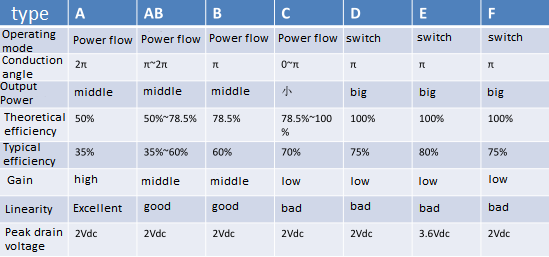
3. Classification
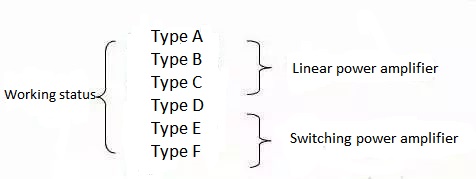
Linear Amplifiers (Class A, AB, B):
Class A: 360° conduction angle, excellent linearity, 25-50% efficiency
Class AB: 180-360° conduction angle, balanced performance, 50-70% efficiency
Class B: 180° conduction angle, improved efficiency over Class A
Switching Amplifiers (Class D, E, F):
Class D: Push-pull switching operation, 75-90% efficiency
Class E: Optimized for high-frequency switching, up to 95% theoretical efficiency
Class F: Harmonic tuning for improved efficiency, 80-90% practical efficiency
Advanced Classes (2025):
Class G/H: Multiple supply voltages for improved efficiency
Envelope Tracking (ET): Dynamic supply modulation, 40-60% average efficiency
Doherty Amplifiers: Peak efficiency at backed-off power levels
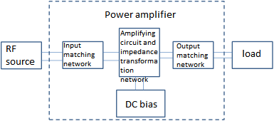
Ⅱ. Circuit Composition
Modern RF power amplifiers consist of several key components working together to achieve optimal performance:
1. Active Devices (Transistors)
Current Technologies (2025):
GaN (Gallium Nitride): High power density, wide bandwidth, excellent thermal performance. Dominant in 5G base stations and radar applications
GaAs (Gallium Arsenide): Superior high-frequency performance, lower noise. Common in mobile devices and satellite communications
SiGe (Silicon Germanium): Cost-effective, good integration. Used in consumer electronics
LDMOS (Laterally Diffused MOS): Still relevant for sub-6GHz high-power applications
2. Bias and Stabilization Circuits
The bias circuit establishes the proper DC operating point for the transistor. Modern implementations include:
Active Bias Networks: Temperature-compensated, adaptive biasing for consistent performance
Digital Bias Control: Microcontroller-based adjustment for optimal efficiency across operating conditions
Envelope Tracking Supplies: Dynamic bias modulation following signal envelope
Stabilization circuits prevent oscillations and ensure reliable operation across temperature and frequency ranges. Modern designs incorporate:
Resistive/capacitive stabilization networks
Ferrite beads for high-frequency isolation
Digital monitoring and adaptive compensation
3. Input and Output Matching Networks
Matching networks optimize power transfer and control bandwidth. Common topologies include:
L-Match: Simple, two-element design for fixed impedance transformation
Pi-Match: Three elements, absorbs parasitic capacitance effectively
T-Match: Handles inductive parasitics, symmetrical design
Distributed Elements: Transmission line-based matching for mmWave frequencies
2025 Advancement: Tunable matching networks using MEMS or varactor diodes enable real-time impedance optimization, improving efficiency across varying load conditions—critical for antenna mismatch scenarios in mobile devices.
Ⅲ. How to Choose the Right RF Power Amplifier
Selecting an appropriate RF amplifier requires careful consideration of multiple parameters:
Key Selection Criteria
Frequency Range: Ensure the amplifier covers your operating frequency with adequate margin. Consider 5G bands (sub-6GHz and mmWave 24-71GHz) for modern applications.
Output Power: Determine required output power considering:
Path loss and link budget
Antenna gain
Regulatory power limits
Efficiency: Critical for battery-powered and thermal-constrained applications. Target >40% for linear applications, >60% for switching designs.
Linearity: Evaluate based on modulation scheme:
OIP3 > +40dBm for high-order QAM
ACPR (Adjacent Channel Power Ratio) < -45dBc for LTE/5G
EVM (Error Vector Magnitude) < 3% for 256-QAM
Bandwidth: Instantaneous bandwidth requirements for wideband signals (e.g., 100MHz for 5G)
Supply Voltage: Match available power supply (3.3V, 5V, 12V, 28V, 48V common)
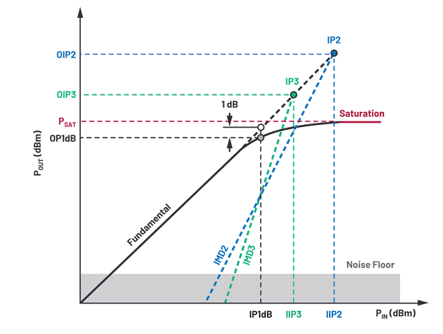
Linearity Parameters
P1dB (1dB Compression Point): Output power where gain drops by 1dB
PSAT (Saturated Power): Maximum output power
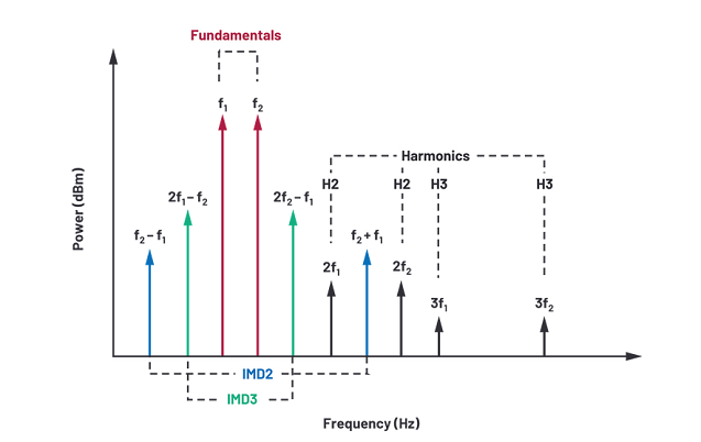
IP3 (Third-Order Intercept Point): Measure of third-order intermodulation distortion
IP2 (Second-Order Intercept Point): Relevant for direct conversion receivers
Ⅳ. Differences Between RF Power Amplifier Types
Low Noise Amplifiers (LNA)
Optimized for minimal noise figure (NF), typically<1dB for modern designs. Essential in receiver front-ends where signal-to-noise ratio is critical. 2025 LNAs achieve noise figures below 0.5dB at sub-6GHz frequencies using advanced GaAs or SiGe BiCMOS processes.
Low Phase Noise Amplifiers
Designed for minimal phase noise contribution, critical in:
Local oscillator (LO) chains
High-performance PLLs
Radar systems
Test equipment
Modern designs achieve phase noise floors below -170dBc/Hz at 1MHz offset.
Power Amplifiers (PA)
Optimized for high output power and efficiency. Current state-of-the-art:
GaN PAs: 100W+ at >50% efficiency for base stations
GaAs PAs: 1-5W at 40-45% efficiency for handsets
Envelope tracking: 50-60% average efficiency with LTE/5G signals
High Linearity Amplifiers
Designed for excellent linearity with complex modulated signals. Features include:
Digital pre-distortion (DPD) compatibility
High OIP3 (>+45dBm)
Low EVM (<2% for 256-QAM)
Wide dynamic range
Variable Gain Amplifiers (VGA)
Provide adjustable gain for:
Automatic gain control (AGC) loops
Dynamic range optimization
Temperature compensation
Modern VGAs offer 40-60dB gain range with 0.5-1dB steps, controlled digitally via SPI/I2C interfaces.
Broadband Amplifiers
Cover multiple octaves (e.g., 0.1-6GHz) with moderate gain (15-20dB). Trade-offs include:
Lower efficiency vs. narrowband designs
Higher noise figure
Excellent versatility for multi-band applications
Gain Blocks
Integrated solutions with matching and bias circuits included. Benefits:
Simplified design and layout
Consistent performance
Reduced time-to-market
50Ω matched input/output
Ⅴ. Frequently Asked Questions (FAQs)
Q1: What is the difference between Class A and Class AB amplifiers?
Class A amplifiers conduct for the full 360° of the input signal cycle, providing excellent linearity but lower efficiency (25-50%). Class AB amplifiers conduct for more than 180° but less than 360°, offering a balance between linearity and efficiency (50-70%). Class AB is more common in modern RF applications due to better power efficiency while maintaining acceptable linearity.
Q2: Why is GaN technology preferred for 5G base station amplifiers?
GaN (Gallium Nitride) offers several advantages: higher power density (5-10x vs. LDMOS), wider bandwidth, better efficiency at high frequencies, and superior thermal performance. These characteristics enable smaller, more efficient 5G base stations with better performance, particularly important for massive MIMO arrays and mmWave frequencies.
Q3: What is envelope tracking and how does it improve efficiency?
Envelope tracking (ET) is a technique that dynamically adjusts the amplifier's supply voltage to match the signal envelope. Instead of using a fixed high supply voltage, ET reduces voltage during low-power portions of the signal, significantly improving average efficiency (40-60% vs. 25-35% for fixed supply) with modern modulated signals like LTE and 5G.
Q4: How do I calculate the required output power for my application?
Calculate using the link budget equation: Required PA Output Power = Desired Received Power + Path Loss - Transmit Antenna Gain - Receive Antenna Gain + System Losses + Margin. Include cable losses, connector losses, and add 3-6dB margin for fading and component variations. Online link budget calculators can simplify this process.
Q5: What is the typical lifespan of an RF power amplifier?
With proper thermal management and operation within specifications, modern RF PAs typically last 10-20 years in fixed installations. Mobile device PAs may experience degradation after 5-7 years due to thermal cycling. Key factors affecting lifespan include operating temperature, duty cycle, and voltage stress. GaN devices generally show better long-term reliability than GaAs at high power levels.
Q6: How important is thermal management for RF power amplifiers?
Thermal management is critical. For every 10°C increase in junction temperature, device lifetime can decrease by 50%. Proper heatsinking, thermal interface materials, and airflow are essential. Modern high-power PAs may require active cooling (fans or liquid cooling) to maintain junction temperatures below 150°C for GaN or 125°C for GaAs devices.
Q7: Can I use a 4G LTE amplifier for 5G applications?
It depends on the frequency bands. For sub-6GHz 5G (using similar frequencies to 4G), many LTE amplifiers can work if they meet linearity requirements for 5G modulation (higher-order QAM). However, mmWave 5G (24-71GHz) requires purpose-built amplifiers. Additionally, 5G's wider bandwidths (up to 100MHz) may exceed some LTE amplifier capabilities.
Q8: What is digital pre-distortion (DPD) and when is it needed?
DPD is a linearization technique that pre-distorts the input signal to compensate for amplifier nonlinearity. It's essential for high-power amplifiers using complex modulation schemes (64-QAM and higher) where efficiency and linearity must be balanced. Modern DPD systems can improve ACPR by 10-15dB, allowing amplifiers to operate closer to saturation for better efficiency while meeting spectral mask requirements.
Conclusion: RF power amplifier technology continues to evolve rapidly in 2025, driven by 5G deployment, IoT expansion, and satellite communications growth. Understanding the trade-offs between efficiency, linearity, bandwidth, and cost is essential for selecting the optimal amplifier for your application. Modern designs increasingly incorporate digital control, adaptive techniques, and advanced semiconductor materials to meet demanding performance requirements while minimizing size, power consumption, and cost.
 UTMEL
UTMEL
We are the professional distributor of electronic components, providing a large variety of products to save you a lot of time, effort, and cost with our efficient self-customized service. careful order preparation fast delivery service
1. What is RF Power Amplifier?
RF power amplifier is an important part of various wireless transmitters. In the pre-stage circuit of the transmitter, the power of the radio frequency signal generated by the modulation oscillator circuit is very small, and it needs to go through a series of amplification, a buffer stage, an intermediate amplifier stage, and a final power amplifier stage to obtain sufficient RF power before it can be fed. Radiate to the antenna. In order to obtain a large enough radio frequency output power, a radio frequency power amplifier must be used. RF amplifiers can be divided into high-gain amplifiers, low-noise amplifiers, and medium-high power amplifiers. The core of the amplifier circuit is the microwave transistor.
2. What factors affect the gain of the RF power amplifier?
Fundamentally, it is determined by the design of the power tube, and different tube core structures determine its maximum gain. After the tube is determined, the gain is affected by the working conditions. For example: input and output matching circuit, load mismatch situation, die operating temperature. In addition, the working type of the power amplifier (Class A, AB, C) will also affect its gain.
3. What is the use of RF amplifier in radar?
Since the amplitude of the signal received by the electromagnetic wave through the antenna is very small, it needs to be amplified by a power amplifier to drive the lower-level circuit, such as a demodulation circuit, etc.
 Introduction to MD8002A Audio AmplifierUTMEL27 March 20259324
The MD8002A is an audio power amplifier that uses a 5V DC power supply to provide 2.0 watts of continuous power to a BTL load with less than 10% distortion. It was created with the aim of providing high-quality o/p control with fewer components. It doesn't use any output coupling capacitors or bootstrap capacitors.
Read More") Understanding the Low Noise Amplifier (LNA)UTMEL20 March 202525841
Understanding the Low Noise Amplifier (LNA)UTMEL20 March 202525841A low noise amplifier is an amplifier with a very low noise figure. It is generally used as a high-frequency or intermediate-frequency preamplifier for various types of radio receivers, as well as amplifying circuits for high-sensitivity electronic detection equipment.
Read More Introduction to Optical AmplifierUTMEL27 March 202510032
An optical amplifier is a subsystem product that can amplify optical signals in optical fiber communication systems. The principle of the optical amplifier is basically based on the stimulated radiation of the laser, which realizes the amplification effect by converting the energy of the pump light into the energy of the signal light.
Read More What is an Inverting Amplifier?UTMEL25 April 202511852
An inverting amplifier is a fundamental configuration of operational amplifiers where the output signal has opposite polarity to the input signal. This configuration uses an operational amplifier with its inverting input terminal receiving the input signal, while the non-inverting terminal is typically connected to ground. The primary function of this circuit is to amplify the input signal while inverting its phase by 180 degrees.
Read More Low-Power Design of Operational AmplifiersUTMEL27 March 20257313
Hello, this is Candy. With the rise in popularity of battery-powered electronics in recent years, analog circuit designers have been increasingly concerned about power usage. This article will cover how to use low-power op amps in system design, as well as low-power op amps with low supply voltage capabilities and their applications, as well as how to read and understand op amp data sheets appropriately. Circuit design with energy-saving technologies for more efficient device choices.
Read More
Subscribe to Utmel !
![M1.5KE180AE3/TR]() M1.5KE180AE3/TR
M1.5KE180AE3/TRMicrochip Technology
![1N5657/TR]() 1N5657/TR
1N5657/TRMicrochip Technology
![NCP360SNAET1G]() NCP360SNAET1G
NCP360SNAET1GON Semiconductor
![0FHM0001ZXJ]() 0FHM0001ZXJ
0FHM0001ZXJLittelfuse Inc.
![JAN1N5907/TR]() JAN1N5907/TR
JAN1N5907/TRMicrochip Technology
![LTC4366CTS8-2#TRMPBF]() LTC4366CTS8-2#TRMPBF
LTC4366CTS8-2#TRMPBFLinear Technology/Analog Devices
![1N5647A/TR]() 1N5647A/TR
1N5647A/TRMicrochip Technology
![MSMCG30A/TR]() MSMCG30A/TR
MSMCG30A/TRMicrochip Technology
![JANTX1N6467US/TR]() JANTX1N6467US/TR
JANTX1N6467US/TRMicrochip Technology
![SMCJ51CA-13-F]() SMCJ51CA-13-F
SMCJ51CA-13-FDiodes Incorporated