
 Product
 Brand
Brand Articles
 Tools
Tools
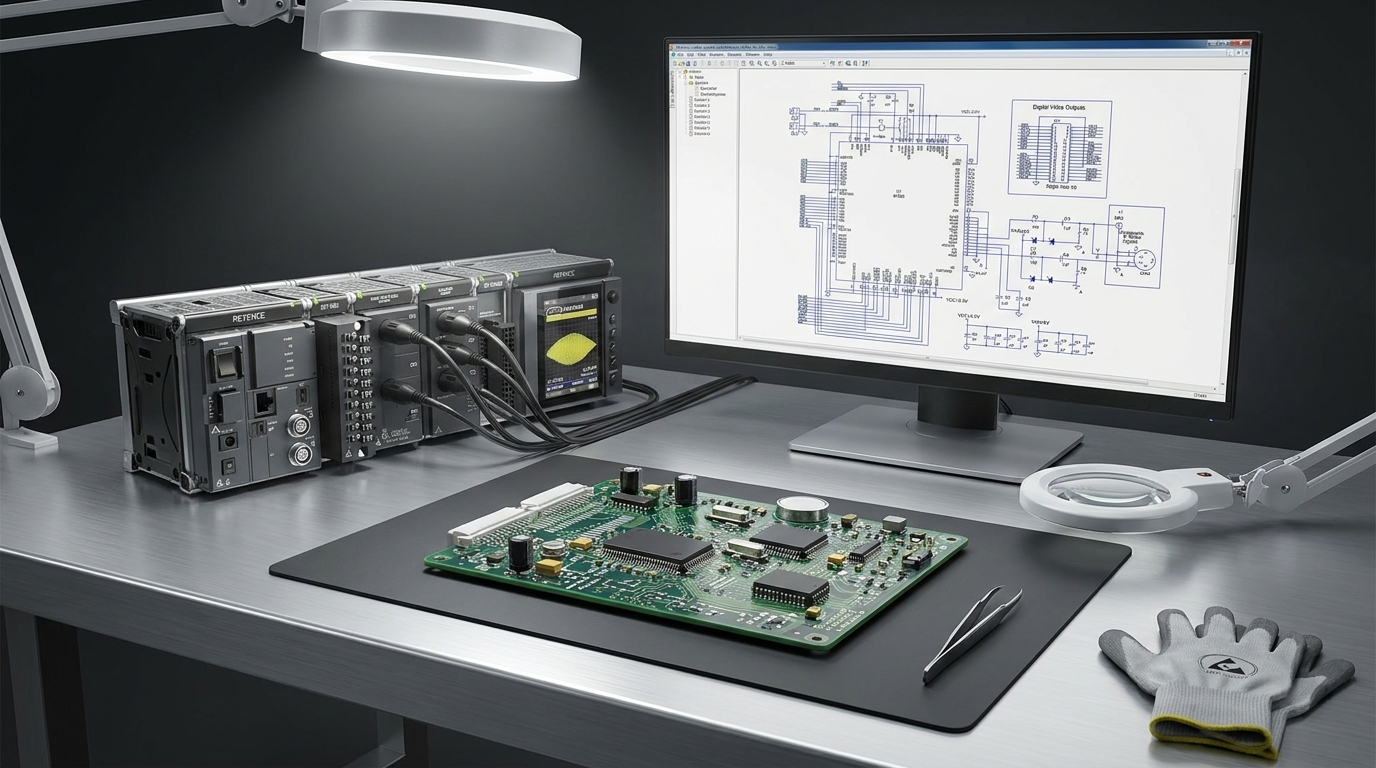
STP9NK60ZFP Power MOSFET: Pinout, Datasheet, and Features


N-Channel Tube 950m Ω @ 3.5A, 10V ±30V 1110pF @ 25V 53nC @ 10V TO-220-3 Full Pack
STP9NK60ZFP is a Power MOSFET with N-channel 600 V, 0.85 Ω typ, and 7 A Zener-protected Super MESH™ in the TO-220 package. This article mainly covers the datasheet, pinout, applications, and more details about STP9NK60ZF.
- STP9NK60ZFP Pinout
- STP9NK60ZFP CAD Model
- STP9NK60ZFP Description
- Specifications
- STP9NK60ZFP Internal Schematic Diagram
- STP9NK60ZFP Features
- STP9NK60ZFP Applications
- STP9NK60ZFP Test Circuit
- STP9NK60ZFP Alternatives
- STP9NK60ZFP Dimension
- Parts with Similar Specs
- STP9NK60ZFP Manufacturer
- Trend Analysis
- Datasheet PDF
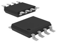
STP9NK60ZFP Pinout

STP9NK60ZFP Pinout
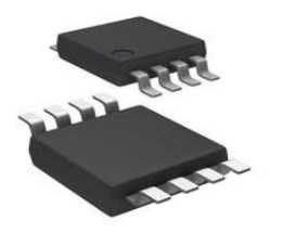
STP9NK60ZFP CAD Model
Footprint

Footprint
STP9NK60ZFP Description
The STP9NK60ZFP is N-channel Zener-protected Power MOSFET developed using STMicroelectronics' SuperMESH™ technology, achieved through optimization of ST's well-established strip-based PowerMESH™ layout. In addition to a significant reduction in on-resistance, this device is designed to ensure a high level of DV/DT capability for the most demanding applications.
Specifications
- TypeParameter
- Lifecycle Status
Lifecycle Status refers to the current stage of an electronic component in its product life cycle, indicating whether it is active, obsolete, or transitioning between these states. An active status means the component is in production and available for purchase. An obsolete status indicates that the component is no longer being manufactured or supported, and manufacturers typically provide a limited time frame for support. Understanding the lifecycle status is crucial for design engineers to ensure continuity and reliability in their projects.
ACTIVE (Last Updated: 8 months ago) - Factory Lead Time12 Weeks
- Mount
In electronic components, the term "Mount" typically refers to the method or process of physically attaching or fixing a component onto a circuit board or other electronic device. This can involve soldering, adhesive bonding, or other techniques to secure the component in place. The mounting process is crucial for ensuring proper electrical connections and mechanical stability within the electronic system. Different components may have specific mounting requirements based on their size, shape, and function, and manufacturers provide guidelines for proper mounting procedures to ensure optimal performance and reliability of the electronic device.
Through Hole - Mounting Type
The "Mounting Type" in electronic components refers to the method used to attach or connect a component to a circuit board or other substrate, such as through-hole, surface-mount, or panel mount.
Through Hole - Package / Case
refers to the protective housing that encases an electronic component, providing mechanical support, electrical connections, and thermal management.
TO-220-3 Full Pack - Number of Pins3
- Weight4.535924g
- Transistor Element Material
The "Transistor Element Material" parameter in electronic components refers to the material used to construct the transistor within the component. Transistors are semiconductor devices that amplify or switch electronic signals and are a fundamental building block in electronic circuits. The material used for the transistor element can significantly impact the performance and characteristics of the component. Common materials used for transistor elements include silicon, germanium, and gallium arsenide, each with its own unique properties and suitability for different applications. The choice of transistor element material is crucial in designing electronic components to meet specific performance requirements such as speed, power efficiency, and temperature tolerance.
SILICON - Current - Continuous Drain (Id) @ 25℃7A Tc
- Drive Voltage (Max Rds On, Min Rds On)10V
- Number of Elements1
- Power Dissipation (Max)30W Tc
- Turn Off Delay Time
It is the time from when Vgs drops below 90% of the gate drive voltage to when the drain current drops below 90% of the load current. It is the delay before current starts to transition in the load, and depends on Rg. Ciss.
43 ns - Operating Temperature
The operating temperature is the range of ambient temperature within which a power supply, or any other electrical equipment, operate in. This ranges from a minimum operating temperature, to a peak or maximum operating temperature, outside which, the power supply may fail.
-55°C~150°C TJ - Packaging
Semiconductor package is a carrier / shell used to contain and cover one or more semiconductor components or integrated circuits. The material of the shell can be metal, plastic, glass or ceramic.
Tube - Series
In electronic components, the "Series" refers to a group of products that share similar characteristics, designs, or functionalities, often produced by the same manufacturer. These components within a series typically have common specifications but may vary in terms of voltage, power, or packaging to meet different application needs. The series name helps identify and differentiate between various product lines within a manufacturer's catalog.
SuperMESH™ - JESD-609 Code
The "JESD-609 Code" in electronic components refers to a standardized marking code that indicates the lead-free solder composition and finish of electronic components for compliance with environmental regulations.
e3 - Part Status
Parts can have many statuses as they progress through the configuration, analysis, review, and approval stages.
Active - Moisture Sensitivity Level (MSL)
Moisture Sensitivity Level (MSL) is a standardized rating that indicates the susceptibility of electronic components, particularly semiconductors, to moisture-induced damage during storage and the soldering process, defining the allowable exposure time to ambient conditions before they require special handling or baking to prevent failures
1 (Unlimited) - Number of Terminations3
- ECCN Code
An ECCN (Export Control Classification Number) is an alphanumeric code used by the U.S. Bureau of Industry and Security to identify and categorize electronic components and other dual-use items that may require an export license based on their technical characteristics and potential for military use.
EAR99 - Terminal Finish
Terminal Finish refers to the surface treatment applied to the terminals or leads of electronic components to enhance their performance and longevity. It can improve solderability, corrosion resistance, and overall reliability of the connection in electronic assemblies. Common finishes include nickel, gold, and tin, each possessing distinct properties suitable for various applications. The choice of terminal finish can significantly impact the durability and effectiveness of electronic devices.
Matte Tin (Sn) - Peak Reflow Temperature (Cel)
Peak Reflow Temperature (Cel) is a parameter that specifies the maximum temperature at which an electronic component can be exposed during the reflow soldering process. Reflow soldering is a common method used to attach electronic components to a circuit board. The Peak Reflow Temperature is crucial because it ensures that the component is not damaged or degraded during the soldering process. Exceeding the specified Peak Reflow Temperature can lead to issues such as component failure, reduced performance, or even permanent damage to the component. It is important for manufacturers and assemblers to adhere to the recommended Peak Reflow Temperature to ensure the reliability and functionality of the electronic components.
245 - Base Part Number
The "Base Part Number" (BPN) in electronic components serves a similar purpose to the "Base Product Number." It refers to the primary identifier for a component that captures the essential characteristics shared by a group of similar components. The BPN provides a fundamental way to reference a family or series of components without specifying all the variations and specific details.
STP9N - Pin Count
a count of all of the component leads (or pins)
3 - Element Configuration
The distribution of electrons of an atom or molecule (or other physical structure) in atomic or molecular orbitals.
Single - Operating Mode
A phase of operation during the operation and maintenance stages of the life cycle of a facility.
ENHANCEMENT MODE - Power Dissipation
the process by which an electronic or electrical device produces heat (energy loss or waste) as an undesirable derivative of its primary action.
30W - Case Connection
Case Connection refers to the method by which an electronic component's case or housing is connected to the electrical circuit. This connection is important for grounding purposes, mechanical stability, and heat dissipation. The case connection can vary depending on the type of component and its intended application. It is crucial to ensure a secure and reliable case connection to maintain the overall performance and safety of the electronic device.
ISOLATED - Turn On Delay Time
Turn-on delay, td(on), is the time taken to charge the input capacitance of the device before drain current conduction can start.
19 ns - FET Type
"FET Type" refers to the type of Field-Effect Transistor (FET) being used in an electronic component. FETs are three-terminal semiconductor devices that can be classified into different types based on their construction and operation. The main types of FETs include Metal-Oxide-Semiconductor FETs (MOSFETs), Junction FETs (JFETs), and Insulated-Gate Bipolar Transistors (IGBTs).Each type of FET has its own unique characteristics and applications. MOSFETs are commonly used in digital circuits due to their high input impedance and low power consumption. JFETs are often used in low-noise amplifiers and switching circuits. IGBTs combine the high input impedance of MOSFETs with the high current-carrying capability of bipolar transistors, making them suitable for high-power applications like motor control and power inverters.When selecting an electronic component, understanding the FET type is crucial as it determines the device's performance and suitability for a specific application. It is important to consider factors such as voltage ratings, current handling capabilities, switching speeds, and power dissipation when choosing the right FET type for a particular circuit design.
N-Channel - Transistor Application
In the context of electronic components, the parameter "Transistor Application" refers to the specific purpose or function for which a transistor is designed and used. Transistors are semiconductor devices that can amplify or switch electronic signals and are commonly used in various electronic circuits. The application of a transistor can vary widely depending on its design and characteristics, such as whether it is intended for audio amplification, digital logic, power control, or radio frequency applications. Understanding the transistor application is important for selecting the right type of transistor for a particular circuit or system to ensure optimal performance and functionality.
SWITCHING - Rds On (Max) @ Id, Vgs
Rds On (Max) @ Id, Vgs refers to the maximum on-resistance of a MOSFET or similar transistor when it is fully turned on or in the saturation region. It is specified at a given drain current (Id) and gate-source voltage (Vgs). This parameter indicates how much resistance the component will offer when conducting, impacting power loss and efficiency in a circuit. Lower Rds On values are preferred for better performance in switching applications.
950m Ω @ 3.5A, 10V - Vgs(th) (Max) @ Id
The parameter "Vgs(th) (Max) @ Id" in electronic components refers to the maximum gate-source threshold voltage at a specified drain current (Id). This parameter is commonly found in field-effect transistors (FETs) and is used to define the minimum voltage required at the gate terminal to turn on the transistor and allow current to flow from the drain to the source. The maximum value indicates the upper limit of this threshold voltage under specified operating conditions. It is an important parameter for determining the proper biasing and operating conditions of the FET in a circuit to ensure proper functionality and performance.
4.5V @ 100μA - Input Capacitance (Ciss) (Max) @ Vds
The parameter "Input Capacitance (Ciss) (Max) @ Vds" in electronic components refers to the maximum input capacitance measured at a specific drain-source voltage (Vds). Input capacitance is a crucial parameter in field-effect transistors (FETs) and power MOSFETs, as it represents the total capacitance at the input terminal of the device. This capacitance affects the device's switching speed and overall performance, as it influences the time required for charging and discharging during operation. Manufacturers provide this parameter to help designers understand the device's input characteristics and make informed decisions when integrating it into a circuit.
1110pF @ 25V - Gate Charge (Qg) (Max) @ Vgs
Gate Charge (Qg) (Max) @ Vgs refers to the maximum amount of charge that must be supplied to the gate of a MOSFET or similar device to fully turn it on, measured at a specific gate-source voltage (Vgs). This parameter is crucial for understanding the switching characteristics of the device, as it influences the speed at which the gate can charge and discharge. A higher gate charge value often implies slower switching speeds, which can impact the efficiency of high-frequency applications. This parameter is typically specified in nanocoulombs (nC) in the component's datasheet.
53nC @ 10V - Rise Time
In electronics, when describing a voltage or current step function, rise time is the time taken by a signal to change from a specified low value to a specified high value.
17ns - Vgs (Max)
Vgs (Max) refers to the maximum gate-source voltage that can be applied to a field-effect transistor (FET) without causing damage to the component. This parameter is crucial in determining the safe operating limits of the FET and helps prevent overvoltage conditions that could lead to device failure. Exceeding the specified Vgs (Max) rating can result in breakdown of the gate oxide layer, leading to permanent damage to the FET. Designers must ensure that the applied gate-source voltage does not exceed the maximum rating to ensure reliable and long-term operation of the electronic component.
±30V - Fall Time (Typ)
Fall Time (Typ) is a parameter used to describe the time it takes for a signal to transition from a high level to a low level in an electronic component, such as a transistor or an integrated circuit. It is typically measured in nanoseconds or microseconds and is an important characteristic that affects the performance of the component in digital circuits. A shorter fall time indicates faster switching speeds and can result in improved overall circuit performance, such as reduced power consumption and increased data transmission rates. Designers often consider the fall time specification when selecting components for their circuits to ensure proper functionality and efficiency.
15 ns - Continuous Drain Current (ID)
Continuous Drain Current (ID) is a key parameter in electronic components, particularly in field-effect transistors (FETs) such as MOSFETs. It refers to the maximum current that can flow continuously through the drain terminal of the FET without causing damage to the component. This parameter is crucial for determining the power handling capability of the FET and is specified by the manufacturer in the component's datasheet. Designers must ensure that the actual operating current does not exceed the specified Continuous Drain Current to prevent overheating and potential failure of the component.
7A - Threshold Voltage
The threshold voltage is a critical parameter in electronic components, particularly in field-effect transistors (FETs). It refers to the minimum voltage required at the input terminal of the FET to turn it on and allow current to flow between the source and drain terminals. Below the threshold voltage, the FET remains in the off state, acting as an open switch. Once the threshold voltage is exceeded, the FET enters the on state, conducting current between the source and drain.The threshold voltage is a key factor in determining the operating characteristics of FETs, such as their switching speed and power consumption. It is typically specified by the manufacturer and can vary depending on the specific type of FET and its design. Designers must consider the threshold voltage when selecting FETs for a particular application to ensure proper functionality and performance.
3.75V - JEDEC-95 Code
JEDEC-95 Code is a standardized identification system used by the Joint Electron Device Engineering Council to categorize and describe semiconductor devices. This code provides a unique alphanumeric identifier for various memory components, ensuring consistency in documentation and communication across the electronics industry. The format includes information about the type, capacity, and technology of the device, facilitating easier specification and understanding for manufacturers and engineers.
TO-220AB - Gate to Source Voltage (Vgs)
The Gate to Source Voltage (Vgs) is a crucial parameter in electronic components, particularly in field-effect transistors (FETs) such as MOSFETs. It refers to the voltage difference between the gate and source terminals of the FET. This voltage determines the conductivity of the FET and controls the flow of current through the device. By varying the Vgs, the FET can be switched on or off, allowing for precise control of electronic circuits. Understanding and properly managing the Vgs is essential for ensuring the reliable and efficient operation of FET-based circuits.
30V - Drain Current-Max (Abs) (ID)
The parameter "Drain Current-Max (Abs) (ID)" in electronic components refers to the maximum current that can flow from the drain to the source terminal of a field-effect transistor (FET) or a similar device. It is a crucial specification that indicates the maximum current handling capability of the component before it reaches its saturation point or gets damaged. This parameter is typically specified in amperes (A) and helps designers ensure that the component can safely handle the expected current levels in a circuit without exceeding its limits. It is important to consider this parameter when designing circuits to prevent overloading the component and ensure reliable operation.
7A - Drain-source On Resistance-Max
Drain-source On Resistance-Max, commonly referred to as RDS(on) max, is a specification for MOSFETs that indicates the maximum resistance between the drain and source terminals when the device is turned on. This parameter is critical for assessing the efficiency of a MOSFET in a circuit, as lower values result in reduced power loss and heat generation during operation. It is measured in ohms and is influenced by factors such as temperature and gate-to-source voltage. Understanding RDS(on) max is essential for optimizing performance in power management and switching applications.
0.95Ohm - Drain to Source Breakdown Voltage
Drain to Source Breakdown Voltage, often denoted as V(BR) D-S, is a critical parameter in electronic components, particularly in field-effect transistors (FETs) and metal-oxide-semiconductor FETs (MOSFETs). It represents the maximum voltage that can be applied between the drain and source terminals of the device without causing breakdown or permanent damage. Exceeding this voltage can lead to excessive current flow, resulting in thermal failure or destruction of the component. It is essential for ensuring reliable operation in circuit designs where high voltages may be encountered.
600V - Pulsed Drain Current-Max (IDM)
The parameter "Pulsed Drain Current-Max (IDM)" in electronic components refers to the maximum current that the device can handle when operated under pulsed conditions. This specification is important for understanding the device's capability to handle short bursts of high current without causing damage. It is typically measured in amperes and is specified for a specific pulse width and duty cycle. Designers use this parameter to ensure that the component can withstand transient current spikes without failing, making it crucial for applications where pulsed operation is common, such as in power electronics and RF circuits.
28A - Height16.4mm
- Length10.4mm
- Width4.6mm
- REACH SVHC
The parameter "REACH SVHC" in electronic components refers to the compliance with the Registration, Evaluation, Authorization, and Restriction of Chemicals (REACH) regulation regarding Substances of Very High Concern (SVHC). SVHCs are substances that may have serious effects on human health or the environment, and their use is regulated under REACH to ensure their safe handling and minimize their impact.Manufacturers of electronic components need to declare if their products contain any SVHCs above a certain threshold concentration and provide information on the safe use of these substances. This information allows customers to make informed decisions about the potential risks associated with using the components and take appropriate measures to mitigate any hazards.Ensuring compliance with REACH SVHC requirements is essential for electronics manufacturers to meet regulatory standards, protect human health and the environment, and maintain transparency in their supply chain. It also demonstrates a commitment to sustainability and responsible manufacturing practices in the electronics industry.
No SVHC - Radiation Hardening
Radiation hardening is the process of making electronic components and circuits resistant to damage or malfunction caused by high levels of ionizing radiation, especially for environments in outer space (especially beyond the low Earth orbit), around nuclear reactors and particle accelerators, or during nuclear accidents or nuclear warfare.
No - RoHS Status
RoHS means “Restriction of Certain Hazardous Substances” in the “Hazardous Substances Directive” in electrical and electronic equipment.
ROHS3 Compliant
STP9NK60ZFP Internal Schematic Diagram

STP9NK60ZFP Internal Schematic Diagram
STP9NK60ZFP Features
Extremely high DV/DT capability
Improved ESD capability
100% avalanche tested
Gate charge minimized
Very low intrinsic capacitances
STP9NK60ZFP Applications
Switching applications
STP9NK60ZFP Test Circuit

Test circuit for resistive load

Gate charge test circuit

Test circuit for inductive load

Unclamped Inductive load test circuit
STP9NK60ZFP Alternatives
4N60, K2996, 07N60, 10N60, K2645, K2141, K3115
STP9NK60ZFP Dimension

STP9NK60ZFP Dimension
Parts with Similar Specs
- ImagePart NumberManufacturerMountPackage / CaseContinuous Drain Current (ID)Current - Continuous Drain (Id) @ 25°CThreshold VoltageGate to Source Voltage (Vgs)Power DissipationPower Dissipation-MaxView Compare
![STP9NK60ZFP]()
STP9NK60ZFP
Through Hole
TO-220-3 Full Pack
7 A
7A (Tc)
3.75 V
30 V
30 W
30W (Tc)
![STP6NK60ZFP]()
Through Hole
TO-220-3 Full Pack
6 A
6A (Tc)
3.75 V
30 V
32 W
30W (Tc)
![STF10N62K3]()
Through Hole
TO-220-3 Full Pack
8.4 A
8.4A (Tc)
3.75 V
30 V
30 W
30W (Tc)
![STP9NK50ZFP]()
Through Hole
TO-220-3 Full Pack
7.2 A
7.2A (Tc)
3.75 V
30 V
30 W
30W (Tc)


STP9NK60ZFP Manufacturer
STMicroelectronics is a French-Italian multinational electronics and semiconductors manufacturer headquartered in Plan-les-Oates near Geneva, Switzerland. The company resulted from the merger of two government-owned semiconductor companies in 1987: "Thomson Semiconductors" of France and "SGS Microelettronica" of Italy. It is commonly called "ST", and it is Europe's largest semiconductor chip maker based on revenue. While STMicroelectronics corporate headquarters and the headquarters for the EMEA region are based in the Canton of Geneva, the holding company, STMicroelectronics N.V. is incorporated in the Netherlands.
Trend Analysis
Datasheet PDF
- Datasheets :
What can be STP9NK60ZFP Power MOSFETs used for?
In the automotive industry, STP9NK60ZFP Power MOSFETs are widely used in automotive electronics. Power MOSFETs (including DMOS, LDMOS, and VMOS) are commonly used for a wide range of other applications.
How does STP9NK60ZFP Power MOSFETs work?
STP9NK60ZFP Power MOSFETs are three-terminal silicon devices that function by applying a signal to the gate that controls current conduction between source and drain.
Are STP9NK60ZFP and 4N60 interchangeable?
Yes, they are all 4A 600v MOS tubes
![LA4440 Power Amplifier: 6W 2-Channel Amplifier, Pinout and Circuit Diagram [Video]](https://res.utmel.com/Images/Article/1c557673-72fd-4beb-b307-0680a3165ac9.jpg) LA4440 Power Amplifier: 6W 2-Channel Amplifier, Pinout and Circuit Diagram [Video]
LA4440 Power Amplifier: 6W 2-Channel Amplifier, Pinout and Circuit Diagram [Video]08 December 202127391
 ADM485 Transceiver : Datasheet, Pinout and Circuit
17 July 20214336
 MK64FN1M0VLQ12 NXP semiconductor 144LQFP: MK64FN1M0VLQ12 VS ATSAM4E16EA-AUR, Datasheet, Pinout
21 January 2022829
 Unveiling the PIC16CE62X OTP 8-bit CMOS MCU with EEPROM Data Memory: Technical Deep Dive
29 February 2024448
 CD4066 Quad Bilateral Switches IC: Equivalent, Pinout and Uses
07 September 20219030
![ATTINY84A-PU AVR series Microcontroller IC 8-Bit 20MHz[FAQ]: Datasheet, Features, and Pinout](https://res.utmel.com/Images/Article/889533d0-63dd-4ec6-8d21-6b346255db18.jpg) ATTINY84A-PU AVR series Microcontroller IC 8-Bit 20MHz[FAQ]: Datasheet, Features, and Pinout
ATTINY84A-PU AVR series Microcontroller IC 8-Bit 20MHz[FAQ]: Datasheet, Features, and Pinout18 March 2022711
![The Overview of LSM6DSL [FAQ]](https://res.utmel.com/Images/Article/59a17e36-1515-4fb1-add5-9ccc80e48790.jpg) The Overview of LSM6DSL [FAQ]
The Overview of LSM6DSL [FAQ]12 July 20212986
 MCP1253 DC/DC Converter: Specifications, Pinout and Datasheet
12 October 20211089
 Nearly 60% of the Industry Believes That the Chip Shortage Will Be Solved in 2023 at the Earliest
21 April 2022963
 How to Select a Power Relay That Fits Your Requirements
10 July 20252810
 Basic Knowledge of Various Types of Mixers
03 January 20236420
 The Proactive Playbook for EOL Component Sourcing: Managing NRND Without Adding Risk
09 June 202699
 Introduction to FinFET
18 March 202130057
 How to Validate a Pin-to-Pin LDO or Voltage Regulator Substitute
10 June 202692
 How to Design a High-precision ADC?
13 December 20212526
 How Big is the DV/DT and DI/DT of the Power Device?
24 April 202210941
STMicroelectronics
In Stock: 200
United States
China
Canada
Japan
Russia
Germany
United Kingdom
Singapore
Italy
Hong Kong(China)
Taiwan(China)
France
Korea
Mexico
Netherlands
Malaysia
Austria
Spain
Switzerland
Poland
Thailand
Vietnam
India
United Arab Emirates
Afghanistan
Åland Islands
Albania
Algeria
American Samoa
Andorra
Angola
Anguilla
Antigua & Barbuda
Argentina
Armenia
Aruba
Australia
Azerbaijan
Bahamas
Bahrain
Bangladesh
Barbados
Belarus
Belgium
Belize
Benin
Bermuda
Bhutan
Bolivia
Bonaire, Sint Eustatius and Saba
Bosnia & Herzegovina
Botswana
Brazil
British Indian Ocean Territory
British Virgin Islands
Brunei
Bulgaria
Burkina Faso
Burundi
Cabo Verde
Cambodia
Cameroon
Cayman Islands
Central African Republic
Chad
Chile
Christmas Island
Cocos (Keeling) Islands
Colombia
Comoros
Congo
Congo (DRC)
Cook Islands
Costa Rica
Côte d’Ivoire
Croatia
Cuba
Curaçao
Cyprus
Czechia
Denmark
Djibouti
Dominica
Dominican Republic
Ecuador
Egypt
El Salvador
Equatorial Guinea
Eritrea
Estonia
Eswatini
Ethiopia
Falkland Islands
Faroe Islands
Fiji
Finland
French Guiana
French Polynesia
Gabon
Gambia
Georgia
Ghana
Gibraltar
Greece
Greenland
Grenada
Guadeloupe
Guam
Guatemala
Guernsey
Guinea
Guinea-Bissau
Guyana
Haiti
Honduras
Hungary
Iceland
Indonesia
Iran
Iraq
Ireland
Isle of Man
Israel
Jamaica
Jersey
Jordan
Kazakhstan
Kenya
Kiribati
Kosovo
Kuwait
Kyrgyzstan
Laos
Latvia
Lebanon
Lesotho
Liberia
Libya
Liechtenstein
Lithuania
Luxembourg
Macao(China)
Madagascar
Malawi
Maldives
Mali
Malta
Marshall Islands
Martinique
Mauritania
Mauritius
Mayotte
Micronesia
Moldova
Monaco
Mongolia
Montenegro
Montserrat
Morocco
Mozambique
Myanmar
Namibia
Nauru
Nepal
New Caledonia
New Zealand
Nicaragua
Niger
Nigeria
Niue
Norfolk Island
North Korea
North Macedonia
Northern Mariana Islands
Norway
Oman
Pakistan
Palau
Palestinian Authority
Panama
Papua New Guinea
Paraguay
Peru
Philippines
Pitcairn Islands
Portugal
Puerto Rico
Qatar
Réunion
Romania
Rwanda
Samoa
San Marino
São Tomé & Príncipe
Saudi Arabia
Senegal
Serbia
Seychelles
Sierra Leone
Sint Maarten
Slovakia
Slovenia
Solomon Islands
Somalia
South Africa
South Sudan
Sri Lanka
St Helena, Ascension, Tristan da Cunha
St. Barthélemy
St. Kitts & Nevis
St. Lucia
St. Martin
St. Pierre & Miquelon
St. Vincent & Grenadines
Sudan
Suriname
Svalbard & Jan Mayen
Sweden
Syria
Tajikistan
Tanzania
Timor-Leste
Togo
Tokelau
Tonga
Trinidad & Tobago
Tunisia
Turkey
Turkmenistan
Turks & Caicos Islands
Tuvalu
U.S. Outlying Islands
U.S. Virgin Islands
Uganda
Ukraine
Uruguay
Uzbekistan
Vanuatu
Vatican City
Venezuela
Wallis & Futuna
Yemen
Zambia
Zimbabwe
![STW9NK90Z]() STW9NK90Z
STW9NK90ZSTMicroelectronics
![STD20NF20]() STD20NF20
STD20NF20STMicroelectronics
![STP80NF10]() STP80NF10
STP80NF10STMicroelectronics
![STW9N150]() STW9N150
STW9N150STMicroelectronics
![STW11NK100Z]() STW11NK100Z
STW11NK100ZSTMicroelectronics
![STH3N150-2]() STH3N150-2
STH3N150-2STMicroelectronics
![STP12NM50FP]() STP12NM50FP
STP12NM50FPSTMicroelectronics
![STW45NM60]() STW45NM60
STW45NM60STMicroelectronics
![STP11NK50ZFP]() STP11NK50ZFP
STP11NK50ZFPSTMicroelectronics
![STP12NM50]() STP12NM50
STP12NM50STMicroelectronics


