

 Product
 Brand
Brand Articles
 Tools
Tools
TLC274 Quad Op-Amp Design Notes: Overcoming Single-Supply Swing Limitations


0.7pA Instrumentational OP Amps 4V~16V ±2V~8V TLC274 14-DIP (0.300, 7.62mm)
Evaluate the TLC274 quad op-amp for single-supply designs. Review key LinCMOS specifications, common-mode limitations, and drop-in rail-to-rail alternatives.
- Key Electrical Characteristics and LinCMOS Advantages
- Navigating Output Swing and Common-Mode Limitations
- Optimizing Sample-and-Hold Circuits
- Primary Applications and Circuit Integration
- Package, Pinout, and Layout Verification
- Direct Alternatives and Rail-to-Rail Upgrades
- Situational Engineering FAQ
- Specifications
- Datasheet PDF
The TLC274 is a precision quad operational amplifier designed for low-power, high-input-impedance analog signal conditioning. Built on Texas Instruments' proprietary LinCMOS technology, this component is frequently selected for battery-powered systems, transducer interfaces, and data acquisition circuits where minimizing input bias current is a primary design goal.
While it remains a staple in legacy and cost-sensitive designs, modern integration requires a strict understanding of its boundary conditions. Engineers must carefully evaluate its asymmetric common-mode input range and output swing constraints before committing it to a new bill of materials (BOM).
This guide examines the core electrical characteristics of the op-amp, explores critical design trade-offs in single-supply environments, and details exact upgrade paths when true rail-to-rail performance is required.
Key Electrical Characteristics and LinCMOS Advantages
The fundamental appeal of the LinCMOS architecture lies in its ability to combine the low power consumption of CMOS with precision specifications that traditionally required bipolar or JFET technologies.
For component selection and circuit qualification, the following specifications dictate the device's operating envelope:
Supply Voltage Limit: The device supports a maximum supply voltage of 16V. It is highly versatile, operating comfortably on either a single supply (e.g., 5V, 12V) or a dual supply (e.g., ±5V).
Input Bias Current: Typically sitting at an ultra-low 1 pA, this is the defining specification for high-impedance applications. It allows the amplifier to interface directly with sensitive transducers without loading the source or introducing significant offset errors.
Speed and Bandwidth: The amplifier offers a gain-bandwidth product (GBP) of 1.7 MHz and a slew rate of 3.6 V/µs. This makes it adequately fast for standard audio frequencies, low-speed sensor polling, and general-purpose active filters, though it will bottleneck high-speed ADC driving.
Channel Density: As a quad operational amplifier, it provides four independent channels in a standard 14-pin configuration, optimizing board space in multi-sensor data acquisition systems.
Navigating Output Swing and Common-Mode Limitations
The most frequent engineering roadblock encountered with this component involves its behavior near the supply rails. Because it is an older-generation CMOS amplifier, it does not feature a modern rail-to-rail input/output (RRIO) topology. Understanding this asymmetry is critical to preventing signal clipping and dynamic range loss.
The Input Common-Mode Trap
The input common-mode voltage range of this amplifier includes the negative rail (or ground, in a single-supply configuration) but does not reach the positive rail.
If you are designing a low-side current sensing circuit where the inputs sit near ground, the amplifier performs exceptionally well. However, if your design requires high-side sensing or involves input signals that swing close to the positive supply (VDD), the internal input stage will saturate, leading to severe phase reversal or clipping. If full-range input tracking is required, a true RRIO amplifier must be substituted.
Output Swing Constraints in 5V Systems
The output stage presents a similar, often more restrictive, challenge. The output voltage can typically only drive to within 1V to 2V of the positive rail.
In a traditional ±15V dual-supply system, losing 1.5V of headroom at the top end is rarely a dealbreaker. However, in a modern 5V single-supply system, an output that clips at 3.5V drastically reduces the available dynamic range for downstream analog-to-digital converters (ADCs). Engineers attempting to drive a 0–5V ADC input will find the top 30% of their scale completely inaccessible.
If your signal requires a full 0–5V swing, you cannot fix this with passive components; you must upgrade the active silicon to a pin-compatible RRIO device like the TLC2274 or LMC6484.
Optimizing Sample-and-Hold Circuits
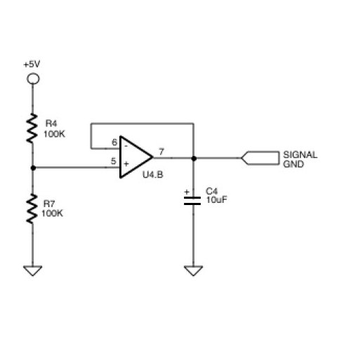
Because of its typical 1 pA input bias current, this amplifier is heavily utilized in sample-and-hold (S&H) circuits, active integrators, and long-time-constant filters. In theory, a 1 pA bias current should prevent the holding capacitor from discharging, allowing the sampled voltage to remain stable for extended periods.
In practice, engineers frequently report unexpected voltage droop and drift in these applications. This is rarely a failure of the op-amp itself, but rather a failure to account for parasitic environmental factors that overwhelm the 1 pA specification.
To achieve the theoretical performance of the silicon, two external factors must be tightly controlled: 1. Capacitor Dielectric Absorption: Standard ceramic capacitors (like X7R or Y5V) exhibit "memory" effects where the dielectric absorbs and releases charge, causing the held voltage to drift. To fix this, S&H circuits utilizing this amplifier must use high-quality, low-leakage capacitors such as NP0/C0G ceramics, polystyrene, or Teflon. 2. PCB Surface Leakage: A 1 pA bias current is easily dwarfed by leakage currents creeping across a slightly contaminated FR4 printed circuit board. To protect the high-impedance inputs, ensure clean PCB layouts. In precision applications, implementing physical guard rings around the input pins—driven to the same potential as the input signal—is strictly required to eliminate parasitic leakage paths.
Primary Applications and Circuit Integration
When the headroom constraints are respected, the device excels in several specific analog domains:
Analog Signal Conditioning: Used to amplify low-level signals from thermistors, photodiode arrays, and pH sensors where high input impedance prevents source loading.
Transducer Interfaces: Ideal for buffering piezo-electric sensors or other high-source-impedance transducers.
Battery-Powered Applications: The LinCMOS technology ensures relatively low quiescent current draw, preserving battery life in remote monitoring nodes.
Active Filters: The 1.7 MHz bandwidth comfortably supports multi-stage Sallen-Key or Multiple Feedback (MFB) low-pass and band-pass filters for sub-100 kHz signals.
Package, Pinout, and Layout Verification
Before releasing a BOM or finalizing a schematic capture, engineers must verify the physical and thermal characteristics of the selected component variant.
The device is available in standard 14-pin packages, including DIP (Dual In-line Package) for prototyping and SOIC/TSSOP for high-density surface mount production. The pinout follows the industry-standard quad op-amp configuration (e.g., Pin 4 is typically VCC/VDD, and Pin 11 is GND/VEE), making footprint verification relatively straightforward.
Verification Checklist:* Temperature Grades: Suffixes dictate the operating temperature range (e.g., commercial vs. industrial). Since exact thermal derating will depend heavily on your PCB copper area and ambient enclosure temperatures, checking the manufacturer's specific curves for your exact suffix is strictly required here. * Decoupling: Despite its relatively low speed, place a 0.1 µF ceramic bypass capacitor as close to the supply pins as physically possible to prevent high-frequency noise injection from the supply rails.
Direct Alternatives and Rail-to-Rail Upgrades
Given the component's age and specific limitations, procurement managers and design engineers often need to evaluate alternatives for either performance upgrades, BOM consolidation, or supply chain resilience.
Be aware that "pin-compatible" does not mean "drop-in equivalent." Moving from a standard CMOS op-amp to a JFET or bipolar device will radically alter bias currents and supply requirements.
| Competitor / Alternate | Technology / Type | Key Differences & Replacement Notes |
|---|---|---|
| TLC2274 | Advanced LinCMOS | The direct TI Upgrade. It offers true rail-to-rail output (RRIO) performance, solving the output swing limitation in 5V single-supply systems while maintaining the low bias current. |
| LMC6484 | CMOS | A highly popular RRIO quad op-amp. Excellent drop-in replacement if full input and output rail-to-rail operation is mandatory. |
| TL074 | JFET-Input | Industry standard for audio. Offers low noise and high speed but requires higher supply voltages (typically dual supplies) and consumes more power. Not a direct single-supply substitute. |
| LM2902 | Bipolar | Extremely cheap, ubiquitous quad op-amp. However, its bipolar inputs have much higher bias currents (in the nanoamp range), which will ruin high-impedance transducer circuits designed for CMOS parts. |
| MC33204 | Bipolar (RRIO) | Rail-to-rail operation, but again, bipolar inputs. Use only if input impedance is not a critical factor in the design. |
Situational Engineering FAQ
Why is my amplifier's output clipping at 3.5V in a 5V single-supply circuit?This is the standard output swing limitation of the architecture. The output stage can only drive to within 1V to 2V of the positive supply rail. To achieve a 5V swing, you must replace the IC with a rail-to-rail output amplifier like the TLC2274.
Can I replace the TLC274 with an LM2902 to reduce BOM costs?Only if your circuit has low source impedance. The LM2902 is a bipolar amplifier with significantly higher input bias current. If your circuit relies on the 1 pA bias current of the LinCMOS part (such as in a sample-and-hold or pH sensor interface), swapping to an LM2902 will introduce massive offset errors and load the sensor.
Does the input common-mode range support ground-sensing?Yes. In a single-supply configuration, the common-mode input range includes the negative rail (ground). This makes it highly effective for low-side current sensing or zero-volt referenced sensor inputs, provided the signal does not attempt to swing near the positive rail.
What causes voltage drift when using this op-amp in a data acquisition front-end?If the amplifier is buffering a hold capacitor, the drift is likely caused by capacitor dielectric absorption or parasitic PCB leakage. Ensure you are using NP0/C0G or polystyrene capacitors, and verify that the PCB layout is clean, ideally utilizing guard rings around the high-impedance input pins.
Watch Tutorial: TLC274
Specifications
Datasheet PDF
- PCN Design/Specification :
- Datasheets :
 DLW21HN900SQ2L CMC 330MA 2LN 90 OHM SMD: Datasheet, Features, and Equivalent Circuit
02 March 20221323
 1N4742A Zener Diodes: Features, Pinout, and Datasheet
18 October 20219668
 BMM150 Sensor: Datasheet, Pinout and Applications
27 August 20215406
 STM32U575VGT6 Price Trends 2025: Best Buying Strategies & Vendor Comparison
05 July 2025484
 STM32H750VBT6: Features, Applications, and Datasheet
31 October 20237695
 H6 vs H7 Battery: Which One Do You Like Better?
01 April 202251148
 ATTINY13V CMOS 8-bit Microcontroller: Features, Pinout and Datasheet
13 January 20221431
 A Comprehensive Guide to LTC7821IUH#PBF DC-DC Switching Controller
06 March 2024299
 Clamp Diodes: Principles, Functions, and Applications
23 March 202660840
 Basic Understanding of Attenuators
15 September 202017997
 Shenzhen: This Year Will Focus on Promoting SMIC and CR Micro 12-inch Project
13 April 20227289
 What is a variable capacitor?
16 April 202567672
 Demand for Automotive Chips Will Surge 300%
09 April 20225829
 What is Brushless DC Motors (BLDC) ?
03 April 20259103
 Voltage Follower: Purpose, Working, and Circuits
27 March 202528913
 Volkswagen CFO: Chip Supply Shortage Will Continue Until 2024
11 April 20224988
Texas Instruments
In Stock: 11
United States
China
Canada
Japan
Russia
Germany
United Kingdom
Singapore
Italy
Hong Kong(China)
Taiwan(China)
France
Korea
Mexico
Netherlands
Malaysia
Austria
Spain
Switzerland
Poland
Thailand
Vietnam
India
United Arab Emirates
Afghanistan
Åland Islands
Albania
Algeria
American Samoa
Andorra
Angola
Anguilla
Antigua & Barbuda
Argentina
Armenia
Aruba
Australia
Azerbaijan
Bahamas
Bahrain
Bangladesh
Barbados
Belarus
Belgium
Belize
Benin
Bermuda
Bhutan
Bolivia
Bonaire, Sint Eustatius and Saba
Bosnia & Herzegovina
Botswana
Brazil
British Indian Ocean Territory
British Virgin Islands
Brunei
Bulgaria
Burkina Faso
Burundi
Cabo Verde
Cambodia
Cameroon
Cayman Islands
Central African Republic
Chad
Chile
Christmas Island
Cocos (Keeling) Islands
Colombia
Comoros
Congo
Congo (DRC)
Cook Islands
Costa Rica
Côte d’Ivoire
Croatia
Cuba
Curaçao
Cyprus
Czechia
Denmark
Djibouti
Dominica
Dominican Republic
Ecuador
Egypt
El Salvador
Equatorial Guinea
Eritrea
Estonia
Eswatini
Ethiopia
Falkland Islands
Faroe Islands
Fiji
Finland
French Guiana
French Polynesia
Gabon
Gambia
Georgia
Ghana
Gibraltar
Greece
Greenland
Grenada
Guadeloupe
Guam
Guatemala
Guernsey
Guinea
Guinea-Bissau
Guyana
Haiti
Honduras
Hungary
Iceland
Indonesia
Iran
Iraq
Ireland
Isle of Man
Israel
Jamaica
Jersey
Jordan
Kazakhstan
Kenya
Kiribati
Kosovo
Kuwait
Kyrgyzstan
Laos
Latvia
Lebanon
Lesotho
Liberia
Libya
Liechtenstein
Lithuania
Luxembourg
Macao(China)
Madagascar
Malawi
Maldives
Mali
Malta
Marshall Islands
Martinique
Mauritania
Mauritius
Mayotte
Micronesia
Moldova
Monaco
Mongolia
Montenegro
Montserrat
Morocco
Mozambique
Myanmar
Namibia
Nauru
Nepal
New Caledonia
New Zealand
Nicaragua
Niger
Nigeria
Niue
Norfolk Island
North Korea
North Macedonia
Northern Mariana Islands
Norway
Oman
Pakistan
Palau
Palestinian Authority
Panama
Papua New Guinea
Paraguay
Peru
Philippines
Pitcairn Islands
Portugal
Puerto Rico
Qatar
Réunion
Romania
Rwanda
Samoa
San Marino
São Tomé & Príncipe
Saudi Arabia
Senegal
Serbia
Seychelles
Sierra Leone
Sint Maarten
Slovakia
Slovenia
Solomon Islands
Somalia
South Africa
South Sudan
Sri Lanka
St Helena, Ascension, Tristan da Cunha
St. Barthélemy
St. Kitts & Nevis
St. Lucia
St. Martin
St. Pierre & Miquelon
St. Vincent & Grenadines
Sudan
Suriname
Svalbard & Jan Mayen
Sweden
Syria
Tajikistan
Tanzania
Timor-Leste
Togo
Tokelau
Tonga
Trinidad & Tobago
Tunisia
Turkey
Turkmenistan
Turks & Caicos Islands
Tuvalu
U.S. Outlying Islands
U.S. Virgin Islands
Uganda
Ukraine
Uruguay
Uzbekistan
Vanuatu
Vatican City
Venezuela
Wallis & Futuna
Yemen
Zambia
Zimbabwe
![LMV722MX]() LMV722MX
LMV722MXTexas Instruments
![LMC6082AIN]() LMC6082AIN
LMC6082AINTexas Instruments
![RC4558P]() RC4558P
RC4558PTexas Instruments
![LMC6482IMM/NOPB]() LMC6482IMM/NOPB
LMC6482IMM/NOPBTexas Instruments
![LM324MX/NOPB]() LM324MX/NOPB
LM324MX/NOPBTexas Instruments
![LM324AM/NOPB]() LM324AM/NOPB
LM324AM/NOPBTexas Instruments
![LMV324IDR]() LMV324IDR
LMV324IDRTexas Instruments
![LMC7101BIM5/NOPB]() LMC7101BIM5/NOPB
LMC7101BIM5/NOPBTexas Instruments
![TLV2372IDR]() TLV2372IDR
TLV2372IDRTexas Instruments
![NE5532P]() NE5532P
NE5532PTexas Instruments


