
 Product
 Brand
Brand Articles
 Tools
Tools
AD9162 RF DAC Integration Notes: JESD204B Configuration and NCO Synchronization


EVAL BOARD FOR AD9162
Explore the AD9162 16-bit RF DAC for wideband systems. Learn how to resolve JESD204B bit inversion conflicts, align NCO phases, and evaluate TI or Teledyne alternatives.
- Core Specifications and RF Synthesis Capabilities
- Deep Dive: Resolving JESD204B Interface and Bit Inversion Conflicts
- Deep Dive: NCO Phase Synchronization Across Multiple Devices
- Managing Clock Asymmetry and Aliasing in 2x NRZ Mode
- Primary Applications
- Evaluating Alternatives and Equivalents
- Datasheet Verification and Package Layout Considerations
- Frequently Asked Questions
- Specifications
- Datasheet PDF
The AD9162 is a high-performance, 16-bit RF Digital-to-Analog Converter (DAC) designed for direct RF synthesis in wideband communications and instrumentation. Capable of supporting data rates up to 6 GSPS and an effective DAC update rate of 12 GSPS, this component is heavily utilized in systems where pushing the first Nyquist zone higher is critical to reducing analog RF filter complexity.
While the headline specifications make the device highly attractive for next-generation broadband and radar applications, successfully integrating a 12 GSPS converter requires strict adherence to high-speed layout principles, precise clocking symmetry, and careful FPGA-to-DAC interface synchronization.
Core Specifications and RF Synthesis Capabilities
Understanding the baseline capabilities of the AD9162 is necessary for frequency planning and determining whether the DAC can directly synthesize your target band without additional upconversion stages.
Resolution: 16-bit
Max Data Rate: 6 GSPS
Max DAC Update Rate: 12 GSPS
Data Interface: JESD204B (8 lanes)
Interpolation Options: Bypassable (1x, 2x, 3x, 4x, 6x, 8x, 12x, 16x, 24x)
The device supports multiple operating modes tailored to different frequency bands. In baseband 1x bypass mode, it covers DC to 2.5 GHz. Switching to 2x nonreturn-to-zero (NRZ) mode extends the usable range from DC to 6 GHz. For higher frequency requirements, Mix-Mode operation allows synthesis from 1.5 GHz up to 7.5 GHz.
The engineering trade-off here is power consumption and clocking demands. Running the DAC at its maximum 12 GSPS update rate in Mix-Mode demands a pristine, ultra-low-jitter clock source; any phase noise in the clock will directly degrade the synthesized RF signal's error vector magnitude (EVM).
Deep Dive: Resolving JESD204B Interface and Bit Inversion Conflicts
One of the most common hurdles engineers face when bringing up the AD9162 is establishing a stable link across its 8-lane JESD204B interface. At 6 GSPS data rates, the physical layer routing is unforgiving, but logical configuration mismatches are an equally frequent source of failure.
A specific pain point during integration is the occurrence of configuration mismatches when setting up JESD204B bit inversion with external FPGAs. Because high-speed differential pairs (SERDES) often need to be swapped at the PCB level to optimize routing and avoid vias, engineers rely on logical bit inversion to correct the polarity.
If the lane polarity is inverted in the hardware layout, the inversion settings must perfectly match between the FPGA IP core and the AD9162 ACE (Analysis | Control | Evaluation) software configuration. A failure to align these settings will cause the JESD204B link training to fail at the Code Group Synchronization (CGS) or Initial Lane Alignment Sequence (ILAS) phases.
Integration strategy:
1. Document all physical P/N lane swaps on the schematic explicitly.
2. Verify that the FPGA transceiver configuration applies the exact corresponding inversion.
3. Cross-check the AD9162 crossbar and inversion registers to ensure the DAC expects the incoming polarity. Do not assume the default FPGA IP settings will automatically negotiate inverted lanes without manual register flags being set on both ends.
Deep Dive: NCO Phase Synchronization Across Multiple Devices
For phased array radars, beamforming infrastructure, and massive MIMO 5G systems, a single DAC is rarely sufficient. Multiple AD9162 chips must operate in parallel, which introduces a critical challenge: synchronizing the output phase of the MAIN Numerically Controlled Oscillator (NCO) across all devices.
If the NCOs power up and begin accumulating phase at slightly different times, the resulting RF outputs will have random phase offsets relative to one another, completely breaking the beamforming array's spatial accuracy.
To fix this, engineers must ensure precise SYSREF alignment and proper NCO reset timing across all DACs. SYSREF is the master timing signal in the JESD204B subclass 1 standard that aligns the local multi-frame clocks (LMFC) across the system.
* The SYSREF signal must be distributed to all AD9162 devices with matched trace lengths (or calibrated delays) to guarantee it arrives within the exact same device clock cycle.
* Once the LMFCs are aligned, the NCO reset command must be triggered synchronously using a synchronized SYSREF edge.
* If your PCB dielectric material has high weave-skew, or if your clock distribution IC introduces varying propagation delays over temperature, you will lose NCO phase determinism.
Managing Clock Asymmetry and Aliasing in 2x NRZ Mode
When operating the AD9162 in 2x NRZ mode to synthesize signals up to 6 GHz, designers often encounter unexpected aliasing behavior and DDR spurs (specifically at Fs/2 - Fout).
This is almost always caused by clock asymmetry. The internal double-data-rate (DDR) clocking mechanism of the DAC relies on a perfectly symmetric 50% duty cycle clock. Any deviation from this symmetry creates timing imbalances between the rising and falling edges, which manifests in the frequency domain as an image spur at the Nyquist boundary minus the output frequency.
To mitigate this, you must account for clock asymmetry in your initial frequency planning. Avoid placing your carrier frequency exactly where the Fs/2 - Fout spur will land. More importantly, ensure the use of high-quality, symmetric clock sources, and avoid routing the clock signal through active components or buffers that might introduce duty-cycle distortion.
Furthermore, clock adjustment registers for image rejection feature complex interdependence, making manual calibration difficult. If you are tuning for image rejection, follow an iterative calibration procedure to tune registers 0x07f, 0x082, and 0x083 sequentially. Attempting to optimize them out of order will result in a frustrating loop of degrading performance.
Primary Applications
The high bandwidth and dynamic range of the AD9162 dictate its use in demanding, high-cost systems where discrete upconversion mixers can be eliminated to save board space and reduce spurious emissions.
DOCSIS 3.1 Cable Modem Termination Systems (CMTS): The DAC easily handles the stringent out-of-band noise requirements of broadband cable infrastructure.
Wireless Communications Infrastructure: Deployed in W-CDMA, LTE, and 5G base stations for direct RF synthesis of wideband carriers.
Instrumentation and ATE: Used in arbitrary waveform generators and automatic test equipment requiring ultra-wide frequency sweeps.
Radars and Jammers: The Mix-Mode capability (up to 7.5 GHz) is particularly useful for X-band and C-band radar architectures when paired with a single block upconverter.
Evaluating Alternatives and Equivalents
Sourcing high-speed RF DACs often requires exploring secondary options due to lead times, cost constraints, or specific architectural preferences. The AD9162 competes in a specialized tier of converters. If you are looking at alternatives, consider the following components, noting that none of these are drop-in replacements:
Texas Instruments DAC38RF8x Series: A strong competitor offering similar direct RF synthesis capabilities. The TI parts often feature different internal PLL structures and interpolator limits. Transitioning to TI requires a complete PCB respin due to entirely different package footprints and JESD204B lane assignments.
Texas Instruments DAC39xx Series: Geared toward slightly different power-to-performance ratios in telecom infrastructure.
Maxim Integrated MAX5881: Offers high-speed performance but may differ significantly in the software API and calibration routines required for image rejection.
Teledyne e2v EV12DS460: A high-end alternative frequently found in aerospace, defense, and space-grade applications. It provides excellent broadband performance but usually carries a different BOM cost and export compliance profile.
When migrating away from the AD9162, the heaviest engineering burden will fall on the FPGA firmware team, who must rewrite the JESD204B link layer and NCO calibration routines.
Datasheet Verification and Package Layout Considerations
Before finalizing your BOM or releasing Gerber files, specific physical and thermal characteristics must be verified.
Operating at 12 GSPS generates significant heat. The AD9162 requires strict thermal management, typically necessitating a dedicated heatsink or a thermal pad tied to a large internal ground plane. Since exact thermal derating will depend heavily on your PCB copper area, layer count, and ambient airflow, checking the manufacturer's specific thermal resistance curves based on your exact operating mode is strictly required here.
Additionally, verify the physical footprint and pinout in your EDA library against the latest manufacturer documentation. High-speed SERDES pins and clock inputs require tightly controlled impedance routing, and any discrepancy in the library footprint will lead to impedance mismatches, reflections, and degraded EVM.
Frequently Asked Questions
Can I replace the AD9162 with a TI DAC38RF8x without modifying the PCB?
No. The TI DAC38RF8x series has a completely different pinout, package dimension, and JESD204B lane configuration. A full schematic overhaul, PCB layout respin, and FPGA firmware rewrite are required.
Why am I seeing large DDR spurs (Fs/2 - Fout) when using 2x NRZ mode?
This is typically caused by clock asymmetry. The internal DDR clocking requires a near-perfect 50% duty cycle. Any skew or duty-cycle distortion from your clock source will generate these specific spurs.
How do I fix JESD204B link failures during the ILAS phase?
Check for bit inversion conflicts. If the high-speed differential lanes were swapped physically on the PCB to ease routing, ensure the exact corresponding logical bit inversion is enabled in both the FPGA IP core and the AD9162 ACE software.
What is the correct sequence for tuning image rejection registers?
Because the clock adjustment registers are highly interdependent, you must follow an iterative, sequential calibration procedure focusing on registers 0x07f, 0x082, and 0x083. Modifying them randomly will prevent convergence on optimal image rejection.
Specifications
Datasheet PDF
- Datasheets :
- Other Related Documents :
- ConflictMineralStatement :
 TPS22965DSGT Load Switch: Layout, Pinout, and Datasheet
28 March 20224082
 MIC2545A Programmable Current-Limit High-Side Switch: Pinout, Equivalent and Datasheet
29 March 2022631
 ADC120 Converter:Datasheet, Application, Pinout
07 September 2021660
 Top Switch Detection Technologies Transforming Automotive Systems
07 June 2025197
 UC3843N SMPS Controller: Pinout, Equivalent and Datasheet
18 March 20224093
 LM321 Op Amp: Circuit, Pinout, and Datasheet
07 October 20214940
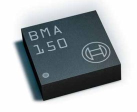 BMA150 Acceleration Sensor: Pinout, Features and Specification
26 April 20212088
 AMD Xilinx Kintex-7 FPGA Series: Architecture Analysis and Design Guide
14 January 2026573
 How much do you know about VR Technology?
01 September 20212335
 Robotics and Semiconductor Industries Face Challenges and Opportunities
09 September 20233767
 Review of Flux-Concentrated Transverse Flux Permanent Magnet Machines
15 December 20232291
 What is a Microcontroller?
30 October 2025117730
 An Overview of JFET
19 August 202011043
 Switch-mode Power Supply Basics
14 December 20208012
 Advanced Aircraft Power Electronics Systems and Influence of Simulation, Standards, and Wide Band-Gap Devices
18 February 20242904
 What is VCSEL?
28 October 202111873
Analog Devices Inc.
In Stock: 659
Minimum: 1 Multiples: 1
Qty
Unit Price
Ext Price
1
$871.311468
$871.31
10
$821.991951
$8,219.92
100
$775.464105
$77,546.41
500
$731.569910
$365,784.96
1000
$690.160293
$690,160.29
Not the price you want? Send RFQ Now and we'll contact you ASAP.
Inquire for More Quantity
![LTC1665CGN]() LTC1665CGN
LTC1665CGNLinear Technology / Analog Devices
![LTC1668IG]() LTC1668IG
LTC1668IGLinear Technology / Analog Devices
![LTC1666IG]() LTC1666IG
LTC1666IGLinear Technology / Analog Devices
![LTC1668CG]() LTC1668CG
LTC1668CGLinear Technology / Analog Devices
![LTC1655CS8]() LTC1655CS8
LTC1655CS8Linear Technology / Analog Devices
![LTC2604IGN]() LTC2604IGN
LTC2604IGNLinear Technology / Analog Devices
![LTC1663IMS8]() LTC1663IMS8
LTC1663IMS8Linear Technology / Analog Devices
![LTC1821ACGW]() LTC1821ACGW
LTC1821ACGWLinear Technology / Analog Devices
![LTC1667CG]() LTC1667CG
LTC1667CGLinear Technology / Analog Devices
![LTC1840IGN]() LTC1840IGN
LTC1840IGNLinear Technology / Analog Devices
