
 Product
 Brand
Brand Articles
 Tools
Tools
How to use 74HC595 Shift Register and interface with Arduino? [FAQ]

Toshiba Semiconductor and Storage
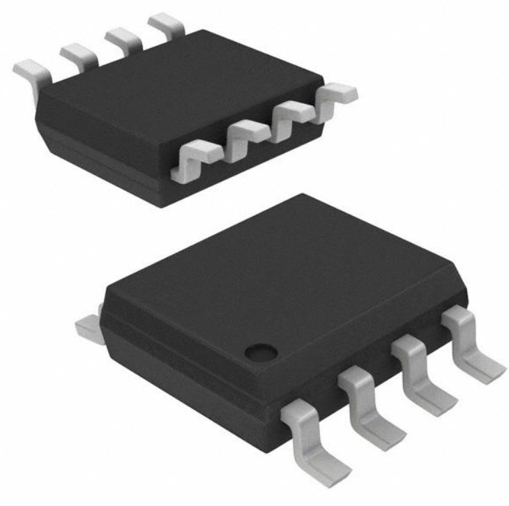
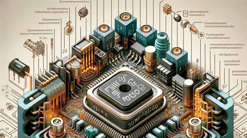
Shift Register -40°C~125°C Shift Register 74HC Series 16-SOIC (0.154, 3.90mm Width)


Shift Register -40°C~125°C Shift Register 74HC Series 16-SOIC (0.154, 3.90mm Width)
74HC595 is a shift register that works on Serial IN Parallel OUT protocol. 74HC595 is used to increase the output pins of your Microcontroller.

How to Add Outputs to an #Arduino using a Shift Register - The Learning Circuit
What is 74HC595?
The 74HC595 is a shift register that uses the Serial IN Parallel OUT protocol to operate. It receives serial data from the microcontroller before sending it out through parallel pins. Using a single chip, we may expand our output pins by eight.
Structure of the 74HC595
The 74HC595 shift register has two main registers :
The shift register
The output register (or data latch or sometimes called a register latch ).
The following is the internal structure of IC 74HC595 :

74HC595 Structurer
The 74HC595 shift register is designed in such a way that when the shift register data is updated using the serial clock (SRCLK) and serial data (SER) inputs, the chip's outputs remain unchanged. In other words, you can send data into the shift register and it will ripple through without changing the state of the output pins. The data is sent from the shift register to the output pins only when the output data clock (latch clock or register clock - RCLK) is strobed.
How Shift Registers Work
When a large number of devices must be interfaced with a microcontroller, the shift register is primarily utilized to overcome the microcontroller's pin shortage. The shift register changes data from one bit to the next in response to the register's clock pulses, and the data it shifts is stored in the register. The shift register has three major pins: one for the clock, another for the latch, and a third for the data.
Explanation of 74HC595 Pinout Diagram

74HC595 Pinout
In the table below, the pin configuration of a single shift register (74HC595) is shown:
| Pins category (From the Left side of the grove) | Pin Numbers | Representation | Description |
| Output pins | 1-7 and 15 | Q1 to Q7, Q0 | Pins at which the device is to be interfaced with the controller |
| Power pins | 8 and 16 | GND, VCC | Pins that will power up the shift register |
| Serial input | 14 | (DS)SERIN | The pin which receives the data from the controller through serial communication |
| Output Enable | 13 | OE | This pin is LOW when voltage is HIGH and vice versa |
| Latch pin | 12 | (ST_CP)RCLK | When this pin is HIGH the data is sent to the output pins and is also stored in the memory |
| clock pin | 11 | (SH_CP) | Clock pin for the shift register |
| RESET pin | 10 | (SH_CP)SRCLR | Pin used to reset the register by giving it a LOW state |
| Interfacing of other registers | 9 | Q7s (QH’) | When more than one registers are to be used, this pin is used |
When to use Shift Register?
Because every microcontroller has a limited number of I/O pins. Shift registers are frequently utilized to save pins on the microcontroller (GPIO).
If you want to control 16 individual LEDs with your project, you'll need an Arduino with 16 pins, This is where the shift register comes in handy if you don't have 16 I/O pins accessible. We can control 16 LEDs with only three I/O pins by connecting two shift registers in series. Not only that, but the more shift registers you chain together, the more pins you save.
The 74HC595 Shift Register IC or any similar shift register for that matter can be used in the following applications:
LED Control
Network Switches
Servers
Power Infrastructure
Industrial Control
Electronic Appliances
Simple Serial-to-Parallel Data Conversion
Capture and Hold Logic
To Use Shift Register with Arduino
Pins 11 (clock input), 12 (storage register clock input or just the latch input ) and 14 (shift register clock input or simply the latch input ) are the three pins of the shift register that must be connected to Arduino (the data input).
The shift register IC will be connected to all 8 LEDs. (See the circuit design section for further information.)
Components Required:
Arduino UNO
74HC595 Shift Register IC
Breadboard
8 X LEDs
8 X 1KΩ Resistors
5V Power Supply
Connecting Wires
Circuit Diagram
We can begin connecting the 74HC595 to our Arduino now that we have a good idea of how it works!
Begin by inserting the shift register on your breadboard, making sure that each side of the IC is on its own side. The pins are 1-8 along the left-hand side from top to bottom with the little U-shaped notch facing upwards, and 16–9 down the right-hand side from top to bottom with the little U-shaped notch facing upwards.
Let's start by connecting pins 16 (VCC) and 10 (SRCLR) to the Arduino's 5v pin, and pins 8 (GND) and 13 (OE) to the Arduino's GND pin. This should keep the IC in its normal state of operation.
The three pins that will control the shift register must then be connected:
Pin 11 (SRCLK) of the shift register to pin 6 on the Arduino
Pin 12 (RCLK) of the shift register to pin 5 on the Arduino
Pin 14 (SER) of the shift register to pin 4 on the Arduino
Now, all we have to do is connect all of the output pins to our LEDs, making sure that a 220 resistor is placed in front of the LEDs to limit current and that the LEDs' cathodes are connected to the ground.
Make sure the LEDs are wired in the correct order when installing them, with QA linked to the first LED and QH connected to the last, else our code will not light up the LEDs in the correct order!
The following is the circuit diagram of the 74HC595 shift register with Arduino:

74HC595 shift register circuit
How 74HC595 Shift Register works?
The shift register 74HC595 features two registers (sometimes known as "memory containers"), each of which holds just 8 bits of data. The first is referred to as the Shift Register, Deep within the IC circuitry, the Shift Register discreetly accepts input.
When we give a 595 a clock pulse, two things happen:
The bits in the Shift Register shift to the left one step. For example, Bit 7 accepts the value from Bit 6, Bit 6 accepts the value from Bit 5, and so on.
The current value on the DATA pin is accepted by Bit 0 in the Shift Register. If the data pin is high on the rising edge of the pulse, a 1 is pushed into the shift register. Otherwise, it's a 0 score.
The contents of the Shift Register are copied into the second register, the Storage/Latch Register, when the Latch pin is enabled. Because each bit of the Storage Register is connected to one of the IC's output pins QA–QH, the outputs change as the value in the Storage Register changes.
How does 74HC595 shift register work?
74HC595 is a shift register that works on Serial IN Parallel OUT protocol. It receives data serially from the microcontroller and then sends out this data through parallel pins. We can increase our output pins by 8 using the single chip. We can also connect more than 1 shift register in parallel.
What is a Shift Register?
A Shift Register is a Serial-to-Parallel Converter IC. It takes a serial input through a single pin (well, technically you need at least 3 pins, which I will talk about later) and converts it into 8-bit parallel output thus effectively reducing the number of interface pins between a Microcontroller and its output devices.
What are the control signals for 74HC595?
The three serial control signals from the microcontroller are:
Serial Data In.
Serial Clock.
Latch Clock.
What can I do with a 74HC595?
74HC595 is a shift register that works on Serial IN Parallel OUT protocol. It receives data serially from the microcontroller and then sends out this data through parallel pins. We can increase our output pins by 8 using the single chip.
 FLIRE5 Infrared Cameras: Datasheet, Price and Benefits
03 August 20211416
 LTM4644IY DC/DC µModule Regulator: Circuit, Pinout, and Datasheet
11 February 20222286
 Unveiling the Microchip PIC18LF1220IP 8-bit Microcontroller: A Comprehensive Analysis
29 February 2024202
 Unlocking the Potential of the PIC18F4520IML Microcontroller
29 February 202496
 LM2903M: Pinout, Datasheet, Comparators
16 March 20222137
 Exploring the Microchip PIC16F62820ISS Microcontroller: Architecture, Modules, and Applications
29 February 2024139
 E91 Energizer AA Alkaline Battery: E91 vs Lithium Batteries, Datasheet, Features
18 January 202211485
 ATmega48PB/88PB/168PB Microcontroller: Technical Insights
29 February 2024195
 Semiconductor Material Industry Guide
21 January 20226025
 Introduction to Pi Filter
19 February 202114798
 Reed Relays: 10 Key Applications in Modern Electronics
04 July 20252502
 What is Solid-state Battery
08 March 20215745
 Ceramic Capacitor Basis: Definition, Types and Parameters
10 March 20225053
 Intel CEO Reiterates: 2024 Will Achieve Process Leadership
05 May 20221229
 What is an Operational Amplifier?
27 March 20253292
 Understanding SiC MOSFET Power Modules and Ensuring its Short-Circuit Safety
15 March 20243811
Toshiba Semiconductor and Storage
In Stock
United States
China
Canada
Japan
Russia
Germany
United Kingdom
Singapore
Italy
Hong Kong(China)
Taiwan(China)
France
Korea
Mexico
Netherlands
Malaysia
Austria
Spain
Switzerland
Poland
Thailand
Vietnam
India
United Arab Emirates
Afghanistan
Åland Islands
Albania
Algeria
American Samoa
Andorra
Angola
Anguilla
Antigua & Barbuda
Argentina
Armenia
Aruba
Australia
Azerbaijan
Bahamas
Bahrain
Bangladesh
Barbados
Belarus
Belgium
Belize
Benin
Bermuda
Bhutan
Bolivia
Bonaire, Sint Eustatius and Saba
Bosnia & Herzegovina
Botswana
Brazil
British Indian Ocean Territory
British Virgin Islands
Brunei
Bulgaria
Burkina Faso
Burundi
Cabo Verde
Cambodia
Cameroon
Cayman Islands
Central African Republic
Chad
Chile
Christmas Island
Cocos (Keeling) Islands
Colombia
Comoros
Congo
Congo (DRC)
Cook Islands
Costa Rica
Côte d’Ivoire
Croatia
Cuba
Curaçao
Cyprus
Czechia
Denmark
Djibouti
Dominica
Dominican Republic
Ecuador
Egypt
El Salvador
Equatorial Guinea
Eritrea
Estonia
Eswatini
Ethiopia
Falkland Islands
Faroe Islands
Fiji
Finland
French Guiana
French Polynesia
Gabon
Gambia
Georgia
Ghana
Gibraltar
Greece
Greenland
Grenada
Guadeloupe
Guam
Guatemala
Guernsey
Guinea
Guinea-Bissau
Guyana
Haiti
Honduras
Hungary
Iceland
Indonesia
Iran
Iraq
Ireland
Isle of Man
Israel
Jamaica
Jersey
Jordan
Kazakhstan
Kenya
Kiribati
Kosovo
Kuwait
Kyrgyzstan
Laos
Latvia
Lebanon
Lesotho
Liberia
Libya
Liechtenstein
Lithuania
Luxembourg
Macao(China)
Madagascar
Malawi
Maldives
Mali
Malta
Marshall Islands
Martinique
Mauritania
Mauritius
Mayotte
Micronesia
Moldova
Monaco
Mongolia
Montenegro
Montserrat
Morocco
Mozambique
Myanmar
Namibia
Nauru
Nepal
New Caledonia
New Zealand
Nicaragua
Niger
Nigeria
Niue
Norfolk Island
North Korea
North Macedonia
Northern Mariana Islands
Norway
Oman
Pakistan
Palau
Palestinian Authority
Panama
Papua New Guinea
Paraguay
Peru
Philippines
Pitcairn Islands
Portugal
Puerto Rico
Qatar
Réunion
Romania
Rwanda
Samoa
San Marino
São Tomé & Príncipe
Saudi Arabia
Senegal
Serbia
Seychelles
Sierra Leone
Sint Maarten
Slovakia
Slovenia
Solomon Islands
Somalia
South Africa
South Sudan
Sri Lanka
St Helena, Ascension, Tristan da Cunha
St. Barthélemy
St. Kitts & Nevis
St. Lucia
St. Martin
St. Pierre & Miquelon
St. Vincent & Grenadines
Sudan
Suriname
Svalbard & Jan Mayen
Sweden
Syria
Tajikistan
Tanzania
Timor-Leste
Togo
Tokelau
Tonga
Trinidad & Tobago
Tunisia
Turkey
Turkmenistan
Turks & Caicos Islands
Tuvalu
U.S. Outlying Islands
U.S. Virgin Islands
Uganda
Ukraine
Uruguay
Uzbekistan
Vanuatu
Vatican City
Venezuela
Wallis & Futuna
Yemen
Zambia
Zimbabwe
![74VHC164FT]() 74VHC164FT
74VHC164FTToshiba Semiconductor and Storage
![74VHC595FT]() 74VHC595FT
74VHC595FTToshiba Semiconductor and Storage
![TC74HC595AFN]() TC74HC595AFN
TC74HC595AFNToshiba
![74VHC165FT]() 74VHC165FT
74VHC165FTToshiba Semiconductor and Storage
![TC74VHC595F(EL,K,F]() TC74VHC595F(EL,K,F
TC74VHC595F(EL,K,FToshiba Semiconductor and Storage
![74HC166D]() 74HC166D
74HC166DToshiba Semiconductor and Storage
![74HC595D(BJ)]() 74HC595D(BJ)
74HC595D(BJ)Toshiba
![TC74HC165AP(F)]() TC74HC165AP(F)
TC74HC165AP(F)Toshiba Semiconductor and Storage
![74HC164D]() 74HC164D
74HC164DToshiba Semiconductor and Storage
![TC74HC165AF(EL,F)]() TC74HC165AF(EL,F)
TC74HC165AF(EL,F)Toshiba Semiconductor and Storage


